Note: Descriptions are shown in the official language in which they were submitted.
CA 02411358 2002-12-10
WO 01/96100 PCT/USO1/40978
1
MULTILAYERED POLYMERIC STRUCTURE
BACKGROUND OF THE INVENTION
Field of Invention
The invention relates generally to electrically conductive polymers a.nd more
particularly to antistatic and electrically protective packaging made of
multilayered
polymeric materials.
Description of the Related Art
Antistatic materials
The sudden discharge of static electricity which may build on a sensitive
electrical component often results in current flow through the component far
exceeding its current carrying capacity. In order to protect and avoid the
damage or
destruction of such components, slow dissipation of the static charge from
these
components is crucial. For this reason, static-sensitive components are
typically
transported and stored on trays or in containers made of "antistatic" material
having a
very high resistance. The high resistance of the material allows electric
charge to
flow through the material only at very low current levels.
Static charges can also impact the quality of signals carried in cables.
Static
charges can induce or modify electrical fields affecting nearby electrical
signals.
Antistatic layers can be incorporated into signal cables to minimize effects
of nearby
static charges.
Antistatic materials used to transport or store static sensitive components
are
generally characterized by a uniform electrically conductive surface having
resistance
in the range of 1x10⁶ to 1x101° ohms per square. Although polymers are
generally
nonconductive, sheets of polymeric compositions containing conductive
impurities or
additives may be made to conduct electricity, and may be used as antistatic
materials.
The additives discussed include but are not limited to metallic powders,
metallic
fibers, ionic conductive polymers, intrinsically conductive polymeric powder
(e.g.,
polypyrrole), carbon fibers or carbon black.
CA 02411358 2005-11-24
51096-5
2
Although prior art packages and trays made of polymeric material are suitable
for dissipating electric charge from sensitive components, they do not protect
the
components from electric charge originating outside of the tray or package. If
a
conventional tray or package of the prior art comes in contact with a current
source
having sufficiently high voltage, electric current can flow through the tray
or package,
and through the components therein, damaging the components. Trays and
packages
made from the single layer polymeric materials of the prior art provide no
means for
shunting current away from the components, and therefor are not suitable for
protecting components against charge emanating outside the tray or package.
Further,
the effectiveness of single Iayer materials of the prior art may be limited to
specific
ranges of voltage or frequency.
Carbon Nanotubes
This invention lies in the field of submicron graphitic carbon fibrils,
sometimes called vapor grown carbon fibers or nanotubes. Carbon fibrils are
IS vermicular carbon deposits having diameters less than LON, preferably less
than O.Stt,
and even more preferably less than 0.2p. They exist in a variety of forms and
have
been prepared through the catalytic decomposition of various carbon-containing
gases
at metal surfaces. Such vermieular carbon deposits have been observed almost
since
the advent of electron microscopy. (Baker and Harris, Chemistry and Physics of
C~ Walker and Thrower ed., VoI. 14, 1978, p. 83; Rodriguezy N., J. Mater.
Researc Vol. 8, p. 3233 (1993)).
In 1976, Endo et al. (see 4berlin, A. and Endo, M., J, of Crystal Growth, Vol.
32 (197, pp. 335-349), elucidated the basic
mechanism by which such carbon fibrils grow. They were seen to originate from
a
metal catalyst particle, which, in the presence of a hydrocarbon containing
gas,
becomes supersaturated in carbon. A cylindrical ordered graphitic core is
extruded
which immediately, according to Endo et al., becomes coated with an outer
layer of
pyrolytically deposited graphite. These fibrils with a pyrolytic overcoat
typically
have diameters in excess of O.lp., more typically 0.2 to 0.5 w.
CA 02411358 2005-11-24
51096-5
3
In 1983, Tennent, U.S. Patent No. 4,663,230,
describes carbon fibrils that are free of a continuous thermal carbon
overcoat and have multiple graphitic outer layers that are substantially
parallel to the
fibril axis. As such they may be characterized as having their cylindrical
axes, the
axes which are perpendicular to the tangents of the curved layers of graphite,
substantially perpendicular to their cylindrical axes. They generally have
diameters
no greater than 0.1 a and length to diameter ratios of at least 5. Desirably
they are
substantially free of a continuous thermal carbon overcoat, i.e.,
pyrolytically
deposited carbon resulting from thermal cracking of the gas feed used to
prepare
them. Thus, the Tennent invention provided access to smaller diameter fibrils,
typically 35 to 700th (0.0035 to 0.070 lt) and to an ordered, "as grown"
graphitic
surface. Fibrillar carbons of less perfect structure, but also without a
pyrolytic carbon
outer layer have also been grown.
The carbon nanotubes which can be oxidized as taught, in this application, are
distinguishable from commercially available continuous carbon fibers. In
contrast to
these fibers which have aspect ratios (L1D) of at least 104 and often 106 or
more,
carbon fibrils have desirably large, but unavoidably finite, aspect ratios.
The diameter
of continuous fibers is also far larger than that of fibrils, being always
>1.0 p and
typically 5 to 7 ~,.
Tennent, et al., US Patent No. 5,171,560,
describes carbon fibrils free of thermal overcoat and having graphitic layers
substantially parallel to the fibril axes such that the projection of the
layers on the
fibril axes eartends for a distance of at least two fibril diameters.
Typically, such
fibrils are substantially cylindrical, graphitic nanotubes of substantially
constant
diameter and comprise cylindrical graphitic sheets whose c-axes are
substantially
perpendicular to their cylindrical axis. They are substantially free of
pyrolytically
deposited carbon, have a diameter less than 0.1 ~ and length to diameter ratio
of
greater than 5. These fibrils can be oxidized by the methods of the invention.
When the projection of the graphitic layers on the nanotube axis extends for a
distance of less than two nanotube diameters, the carbon planes of the
graphitic
CA 02411358 2005-11-24
51096-5
4
nanotube, in cross section, take on a herring bone appearance. These are
termed
fishbone fibrils. Geus, U.S. Patent No. 4,855,091,
provides a procedure for preparation of fishbone fibrils substantially free of
a
pyrolytic overcoat. These carbon nanotubes are also useful, in the practice of
the
invention.
Carbon iianotubes of a morphology similar to the catalytically grown fibrils
described above have been grown in a high temperature carbon arc (Iijima,
Nature,
354, 56, 1991). It is now generally accepted (Weaver, Science, 265. 1994) that
these
arc-grown nanofibers have the same morphology as the earlier catalytically
grown
fibrils of Tennent. Arc grown carbon nanofibers after colloquially referred to
as
"bucky tubes", are also useful in the invention.
Carbon nanotubes differ physically and chemically from continuous carbon
fibers which are commercially available as reinforcement materials, and from
other
forms of carbon such as standard graphite and carbon black. Standard graphite,
because of its structure, can undergo oxidation to almost complete saturation.
Moreover, carbon black is amorphous carbon generally in the form of spheroidal
particles having a graphene structure, carbon layers around a disordered 20
nucleus.
The differences make graphite and carbon black poor predictors of nanotube
chemistry.
AaEreaates of Carbon Nanotubes
As produced carbon nanotubes may be in the form of discrete nanotubes,
aggregates of nanotubes or both.
Nanotubes are prepared as aggregates having various morphologies (as
determined by scanning electron microscopy) in which they are randomly
entangled
with each other to form entangled balls of nanotubes resembling bird nests
("BN"); or
as aggregates consisting of bundles of straight to slightly bent or kinked
carbon
nanotubes having substantially the same relative orientation, and having the
appearance of combed yam ("CY'~ e.g., the longitudinal axis of each nanotube
(despite individual bends or kinks) extends in the same direction as that of
the
surrounding nanotubes in the bundles; or, as, aggregates consisting of
straight to
CA 02411358 2005-11-24
51096-5
slightly bent or kinked nanotutxs which are loosely enrangrea vmn each over w
roan
an "open net" ("ON's structure. In open net structures the extent of nanotube
entanglement is greater than observed in the combed yarn aggregates (in which
the
individual nanotubes have substantially the same relative orientation) but
less than
5 that of bird nest.
The morphology of the aggregate is controlled by the choice of catalyst
support.. Spherical supports grow nanotubes in all directions leading to the
formation
of bird nest aggregates. Combed yarn and open nest aggregates are prepared
using
supports having one or more readily cleavable planar surfaces, e.g., au iron
or
iron-containing metal catalyst particle deposited on a support material having
one or
more readily cleavable siafaces a~ a surface area of at least 1 square meters
per
gram. Moy eE al., U.S. Application Serial No. 08/469,430 entitled "lmpmved
Methods and Catalysts for the Manufacdu~e of Carbon Fibrils", filed June 6,
1995,
describes namotubes prepared as aggregates having
various morphologies (as determined by scanning electron microscopy).
Further details regarding the formation of carbon nanotube or nanofiber
aggregates may be found in the disclosure of U.S. Patent No. 5,165,909 to
Tennent;
U.S. Patent No. 5,456,897 to Moy et al.; PCT Publication No. WO 89/07163; and
PCT
Publication No. WO 91/05089.
OBJECTS OF THE INVENTION
It is therefore an object of the invention to provide an improved
pa~aging material which will protect sensitive electric components from damage
or
don due to elech~osfatic disc)~rge.
CA 02411358 2005-11-24
51096-5
6
It is a further object of the invention to provide
improved packages and carrying trays for electrical
components.
It is a further object of the invention to provide
improved shielding for signal carrying cables.
SUN~1ARY OF THE INVENTION
A packaging material is provided having multiple
polymeric layers. The packaging material may take a form of
a tray, a package or a container for an electronic component
or a form of a protective covering for an electrical current
carrying cable or the like. Each layer comprises a mixture
of a polymer and carbon fibrils. The multilayered material
has an inner layer with a uniform surface resistance
preferably in the range of 1x10⁵ or 1x10⁶ to 1x10¹² ohms per
square, more preferably in the range of 1x10⁶ to 1x101° ohms
per square, and an outer layer with a surface resistance
lower than that of the inner layer, desirably at least one
order of magnitude. The inner and outer layers may be
directly in contact with one another, or there may be one or
more intermediate layers of conductive material between
them. Each intermediate layer could be made of any material
(such as an adhesive) having preferably a surface resistance
of at least 101° ohms per square. The surface resistance of
the packaging material (i.e., the outer surface) varies from
10°'S to 101° ohms per square, preferably from 101 to 108 ohms
per square, more preferably from 101 to 106 ohms per square.
The carbon fibrils in the outer and inner layers may be
contained generally at concentrations of from 0.25 to 35o by
weight, preferably 1 to 150, more preferably 2 to 7o by
weight.
CA 02411358 2005-11-24
51096-5
6a
In a two-layer polymeric structure, the first
(= inner) layer preferably contain a polymer having 0.250
to 250, preferably 1% to 50, by weight of carbon fibrils.
This concentration of fibrils provides the antistatic layer
with a surface resistance preferably in the range of 1x10⁶
to 1x101° ohms per square. The second (= outer) layer may
contain 2o to 350, preferably 2o to 150, more preferably 20
to 70, by weight of carbon fibrils, thereby providing a lower
resistance relative to the first antistatic layer. Each
polymeric layer can have a thickness from about 0.5 mils to
about 175 mils and preferably from about 5 mils to about
30 mils. The entire multilayered polymeric structure can be
of whatever thickness is desirable for a given application.
For example, the structure of the invention can be from
about 1 mil to about 250 mils, preferably from about 2 mils
to about 100 mils and most preferably from about 10 mils to
about 60 mils.
A third polymeric layer may be provided in surface
contact with the first and second layers. The third layer
may contain from about 0.250 to about 35o by weight of carbon
fibrils.
Once each of the polymeric compositions comprising
the various layers of the invention are prepared, they are
combined to form a composite multilayered material. If the
separate layers of polymeric composition are allowed to cure
prior to being joined, the combining process consists of
applying heat and
CA 02411358 2002-12-10
WO 01/96100 PCT/USO1/40978
7
pressure which causes the separate layers to fuse together. It is, however,
preferred
that the separate layers of polymeric material are joined prior to curing.
This may be
accomplished via a coextrusion process, where two or more polymeric
compositions
are forced through a single aperture. The multilayered material produced by
coextrusion may either be allowed to cure as a flat sheet, or may be placed
into molds
in the form of a desired end-product, i.e. a tray. Each polymeric layer can be
processed according to any applicable kind of polymer processing, it being
understood that the carbon fibril loading does not limit its processability.
As used herein to "cure" or "curing" refers to a process of conversion
of raw or reactive polymer systems to a finished and useful condition usually
by
transfer of heat and/or application of chemicals which induce physical and/or
chemical changes. Cooling of a molten polymeric composition into a solid layer
or
sheet is an example of curing. Another example of curing is the process of
crosslinking a thermosetting product.
The polymeric material of the invention may be formed into any one of
a number of shapes or configurations suitable for the transport and/or storage
of
sensitive electrical components, i.e. trays and packages. When the material of
this
invention is formed into a tray or package, the antistatic layer of the
material is
situated such that it faces the inside of the tray or package, and comes
directly in
contact with the component. A more conductive polymeric layer of the material
forms the outside surface of the tray or package.
An advantage of having the outer layer of the multilayered material
more conductive than the inside antistatic layer is that the outer layer acts
as a shunt
for any electric current originating outside of a tray or package made of the
material.
Should a source of electric charge come in contact with the outside surface of
a tray or
package made of the multilayered material, the outer layer will conduct the
current to
a point on the outer surface where the current rnay leave the material. The
relatively
higher resistance of the inner antistatic layer impedes current flow through
that layer
and into components which may be present on the other side.
CA 02411358 2002-12-10
WO 01/96100 PCT/USO1/40978
8
The multilayer materials can be used in other applications where a
gradient in electrical properties is desired. Changes in the in concentration
of fibrils
can lead to changes in both the conductivity and the permitivity of the
resulting
composite. Other applications include: dielectric lenses made of layers with
different
levels of carbon fibrils; field limiting insulation layers for cables or
electronic parts;
and selective shielding or EMI bandpass filters for cables or signal carrying
lines.
In these examples, the different levels of carbon fibrils in the layers
asymmetrically modifies the flow of current or charge perpendicular to the
layers or
modifies electrical fields.
BRIEF DESCRIPTION OF THE FIGURES
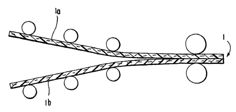
Fig. 1 shows a cross-section of a two Iayer polymeric material
according to the''invention.
Fig. 2 shows a tray made from the two layer' polymeric material of
Fig. 1.
Fig. 3 shows two layers made of polymeric compositions having fibrils
therein being combined to form the two layer conductive polymeric material of
Fig. 1.
Fig. 4 is a test set-up diagram of a molded tensile bar utilized for
measuring DC resistance through the volume of samples in example 1 to 9.
DETAILED DESCRIPTION OF THE INVENTION
In a preferred embodiment of the invention, the material has two
layers, as shown in the cross-sectional view of Fig. 1. The polymeric material
1 of the
invention is a composite of a first layer la and a second layer lb, each layer
being a
mixture of carbon fibrils in a polymer. The electrical resistance of each
polymeric
composition is inversely related to the concentration of fibrils in the
composition, i.e.,
the higher the concentration of fibrils, the lower the electrical resistance
of the
composition. Therefore, the first layer la of polymeric material, with a 2.5%
by
CA 02411358 2002-12-10
WO 01/96100 PCT/USO1/40978
9
weight concentration of carbon fibrils, has a surface resistance of about 1x10
ohms
per square. The second layer lb, having a fibril concentration of 5.0% has a
surface
resistance of only about 1x10⁴ ohms per square.
Carbon fibrils are typically in the form of vermicular tubes with
graphitic outer layers disposed substantially concentrically about the
cylindrical axis
of the fibril. Preferably, the fibrils are substantially free of a
pyrolytically deposited
thermal carbon overcoat.
Carbon fibrils have a length-to-diameter ratio of at least 5, and more
preferably at least 100. Carbon fibrils are carbon filaments having diameters
less than
500 nanometers. Even more preferred are fibrils whose length-to-diameter ratio
is at
least 1000. The wall thickness of the fibrils is about 0.1 to 0.4 times the
fibril external
diameter which is preferably between 3.5 and 75 nanometers. In applications
where
high strength fibrils are needed, e.g., where the fibrils are used as
reinforcements, the
external fibril diameter is substantially constant over its length.
Generally, preferred classes of polymers used for this invention include
thermosets, thermoplastics, elastomers and inorganics. Certain polymeric
alloys,
defined as two or more miscible or partially miscible polymers, and blends,
defined as
discrete non-miscible phases, are also preferred. Specific examples of
thermosets and
elastomers include polyurethanes, natural rubber, synthetic rubber, epoxy,
phenolic,
polyesters, polyamides, and silicones. Specific examples of thermoplastics
include
polyacetal, polyacrylic, acrylonitrile-butadiene-styrene, polycaxbonates,
polystyrenes,
polyethylene, styrene acrylonitrile, polypropylenes, polyethylene
terephthalate,
polybutylene terephthalate, polyamide (6, 6/6, 6/10, 6/12, 11 or 12),
polyamide-imides, polyarylates, polyurethanes, thermoplastic olefins (i.e.,
polypropylene/impact modifiers such as ethylene, propylene and rubber),
thermoplastic elastomers, polyaxylsulfone, polyethersulfone, polyphenylene
sulfide,
polyvinyl chloride, chlorinated polyvinyl chloride, polysulfone,
polyetherimide,
polytetrafluoro ethylene, fluorinated ethylene propylene, perfluoroalkoxy,
polychlorotrifluoro ethylene, ethylene tetrafluoro ethylene, polyvinylidene
fluoride,
polyvinyl fluoride, polyetherketone, polyether etherketone and. polyether
ketone ether
CA 02411358 2002-12-10
WO 01/96100 _ PCT/USO1/40978
ketone. Specific examples of alloys and blends include acrylonitrile-
butadiene-styrene/polyamide, polycarbonate/acrylonitrile-butadiene-styrene,
acrylonitrile butadiene styrene/polyvinyl chloride, polyphenylene
ether/polystyrene,
polyphenylene ether/polyamide, polysulfone/acrylonitrile-butadiene-styrene,
5 polycarbonate/thermoplastic urethane, polycarbonatelpolyethylene
terephthalate,
thermoplastic elastomer alloys, polyamide/elastomers, polyester/elastomers,
polyethylene terephthalate/polybutyl terephthalate; acetal/elastomer,
styrene-malefic-anhydride/acrylonitrile-butadiene-styrene, polyether
etherketone/polyethersulfone, polyethylene/polyamide and polyethylene/acetal.
10 Specific examples of inorganic polymers include phosphorus based compounds
and
silicons.
In a preferred embodiment of the invention, the polymer comprises a
blend of polymers possessing advantageous properties and a compatibilizer or a
compatibilizer with a modifying resin for facilitating the blending of the
polymers.
Specific examples of such blends include polyphenylene ethers (PPE) or
polyphenylene oxides (PPO) with polyamides (e.g., nylons) or polycaxboxylic
reactants. Examples of such polymer blends with compatibilizers or
compatibilizers
and modifying agents are described in U.S. Pat. Nos. 4,988,775 and 5,132,365
and in
European Patent Application Nos. 90124310.5, 90300841.5, 91112496.4 and
92109100.5.
The polymeric compositions comprising each of the various layers of
the multilayered structure of this invention are made by known methods, such
as those
described in U.S. Pat. Nos. 5,643,502, 5,651,922 and 5,591,382 to Nahass et
al. U.S.
Patent Nos. 5,591,382; 5,651,922; and 5,643,502 all to Nahass et al. disclose
a
polymeric composition having improved toughness and conductivity which
includes
carbon fibrils, at least a portion of which are in the form of aggregates,
substantially
all of which aggregates are less than 35 pm in diameter. A method for
preparing this
polymeric composition is also disclosed. The method includes mixing the carbon
fibrils, most of which are in the form of aggregates, with a polymeric
material by
applying shear to break down the aggregates and distribute them in the
polymeric
CA 02411358 2005-11-24
51096-5
11
material until substantially all of the aggregates are less then 35 pm in
diameter.
One method of combining layers la and lb involves first shaping each
of the compositions into individual flat sheets and allowing the sheets to
cure. After
curing, the sheets are pressed together under conditions of high heat and
pressure,
causing them to fuse to one another. Conductive adhesives may also be used to
join
separate sheets of polymeric composition to one another.
Another method is to insert or over-mold the two layers. In this
process an injection molding machine is used to mold the first layer. The
resultant
part is then placed into a second mold where the second layer is then molded
onto the
first. The heat from the second layer causes a melt-bond to form between the
first and
second layers. In this way the layers are cured sequentially. The same effect
can also
be achieved using a special two-shot or mufti-shot molding machine. This is an
apparatus that has two or more barrels that inject polymeric materials into
the same
mold. Materials with different conductivities are placed in different barrels
and
injected into the mold separately to form a two or more layered part.
Once the polymeric compositions constituting each of the layers of the
multilayered polymer structure are prepared, they are preferably combined in a
coextrusion process as schematically depicted in Fig. 3.
In this preferred process, two or more viscous materials are combined
into a multilayered product. The polymeric compositions of the first and
second
layers la and lb are forced through an aperture before either composition has
had a
chance to cure. This forms a multilayered sheet of polymeric compositions
which can
be placed in a mold. A similar process can be used to coextrude multilayer
tubes or
jackets for cables or wires.
Fig. 2 shows a tray 3 made from the multilayered material of this
invention. The first layer 1 a of the material forms the inside antistatic
surface of the
tray 3. A carbon fibril coacentration of 2.5% by weight provides the inside
layer with
a surface resistance of about 1x10' ohms per square. The high level of surface
CA 02411358 2005-11-24
51096-5
12
resistance of the inside layer la allows for the slow dissipation of any
electro-static
charge which may build on components present inside the tray 3. This charge is
dissipated through the outer layer lb which is in electrical contact with the
inner layer
la
The second layer 1 b forms the outside surface of the tray 3 and has a
surface resistance of about 1x10⁴ ohms per square. The second layer contains
about
5% by weight of carbon fibrils, and due to the lower resistance of layer 1 b
relative to
1 a, layer 1 b reduces the risk of electrical charge flowing from outside the
tray into the
tray and damaging components therein. Layer lb acts as a shunt guiding current
away
from the sensitive components inside the tray. Item 4 in Fig. 2 represents an
electrical ,
component which can be carried by using tray 3.
The multilayered polymeric material of this invention may be formed
into any shape or configuration including trays, packages, boxes, and the like
by
injection molding, blow molding, RIM, or any other method commonly known for
shaping polymeric materials. The antistatic properties of the packaging
material of
the invention are measured according to the procedure described in ASTM D-257.
EXAMPLES
The following examples serve to provide further appreciation of the
invention but 5 are not meant in any way to restrict the effective scope to
the
invention.
Examules 1- 9
Masterbatch compositions containing 15% fibril loading were prepared
according to methods described in the examples section of U.S. Patent No.
5,651,922
to Nahass et al. Masterbatch formulations were
prepared having 15% by weight carbon fibrils obtained from bird's nest (BN)
aggregates and 85% polyethylene terephtalate modified with
cylcohexanedimetbanol
(PETG). Other masterbatch compositions included 15% by weight carbon fibrils
from bird's nest type aggregates and 85% polybutylene terephtalate (PBT). Yet
other
masterbatch composition were prepared to include 15% by weight carbon fibrils
from
CA 02411358 2005-11-24
51096-5
13
bird's nest type aggregates and 0.5% by weight polytetrafluoroethylene (PTFE)
and
the balance PETG.
The above masterbatch compositions were used to make other
formulations as listed in Table 1 below. For example, to make a PETG/SBN
product
33.5% PBT/15BN was mixed with 66.7% PETG polymer. PBT and PETG
traps-esterify to form a hybrid mixture of two polymers with a single flow
transition
temperature and are crystalline in nature. The impact modifier (I11~ used in
these
formulations was rubber. For example, formulation 7 of table 1 contains 2% by
weight impact modifier, 5% by weight carbon fibrils from bird's nest
aggregates and a
hybrid mixture of 28 wt'/o PBT and 65 wt% PETG. Electrical properties for each
formulation, such as volume and surface resistivity were measured and are
listed for
each formulation in Table 1 below.
Table 1
ExsmpkFormulationMasterbatc6Volnme Surface Resistivity
Rnistivityo6m/aqnare
ohm-em
1 PETG/21M/SBNPETG/15BN 6.63E+02 2.86E+0$
2 PETG/4IM/SBNPETG/lSBN 5.80E+02 7.71E+O6
3 PETGI61M/SBNPETG/ISBN 930E+02 S.OOE+06
4 PETGf2IM15BNPETGIO.SPTFE/15BN230E+03 1.90E+06
5 PETG/41M/SBNPETG/O.SPTFE/lSBN6.SOE+02 3.70E+06
PETG/6IM/SBNPETG/O.SPTFFJ15BN1.40E+02 4.OOE+06
7 PETG/21M/SBNPBT/ISBN 1.OOE+02 . 3.90E+p5
8 PETG/41M/SBNPBTlISBN 8.74E+02 1.17E+07
9 PETG/tilH!/SBNPBT/15BN 8.46E+02 . 837E+p4
DC resistance through the volume of the samples was measured at 2
volts and converted to volume resistivity using the formula shown with the
test set-up
diagram in Figure 4. Electrodes were painted on each end 5 of injection molded
tensile bars with silver conducting paint after cutting away the tabs from
each end.
The leads of a multi-meter were then contacted with the silver paint electrode
strips 2a
and 2b on the sample in order to obtain surface resistivity measurements and
with the
silver paint electrode strips 3a and 3b in order to obtain vblume resistivity
measurements. In Figure 4, d is the electrode spacing for surface resistivity
test, 1 is
the electrode spacing for volume resistivity test, w is the electrode width
and t is the
CA 02411358 2002-12-10
WO 01/96100 PCT/USO1/40978
14
sample thickness, all values are measured in centimeters. Based on the
foregoing
variables, the surface and volume resistivity are calculated as follows:
surface resistivity (ohm/square) = resistance [ohm]/(d [cm]/w [cm])
volume resistivity (ohm-cm) = resistance [ohm] xt [cm]/(1 [cm]/w
[cm])
Discussion of Experimental Results
Any one of the formulations above can be combined with another to
form a bilayered polymeric structure useful in forming the packaging material
of the
present invention. For example, a bilayered polymeric structure can be made by
coextrusion or lamination with a conductive adhesive between the layers by
overmolding or by two-shot molding. The resulting bilayered structure is then
thermoformed into a tray wherein the layer prepared from composition 1 is the
inside
layer having the higher surface resistivity.
Although the invention has been descxibed with reference to specific
examples, they should not be construed as limiting since they are merely
illustrative
of the invention. One of skill in the art may alter the described examples
without
departing from the spirit or scope of the invention