Note: Descriptions are shown in the official language in which they were submitted.
1 ~-UO-GVUG -.~ IVUU 1 UULC
CA 02412169 2002-12-09
1
Addressing of memory matrix
The present invention concerns a method of driving a passive
matrix-addressable display or memory array of cells comprising an
electrically polarizable material exhibiting hysteresis, in particular a
ferroelectric material, wherein the polarization state of individual,
separately
selectable cells can be switched to a desired condition by application of
electric potentials or voltages to word and bit lines forming an addressing
matrix, and wherein the method comprises establishing a voltage pulsing
protocol with n voltage or potential levels, n >_ 3, such that the voltage
pulsing protocol defines a timing sequence for individually controlling the
voltage levels applied to word and bit lines of the matrix in a
time-coordinated fashion, arranging said timing sequence to encompass at
least two distinct parts, including a "read cycle" during which charges
flowing between said selected bit lines) and the cells connecting to said bit
lines) are sensed, and a "refresh/write cycle" during which polarization
states) in cells connecting with selected word and bit lines are brought to
correspond with a set of predetermined logical states or data values.
Particularly the present invention concerns pulsing protocols for the
addressing of individual crossing points in passive matrices used for data
storage and display purposes. A major concern is the avoidance of disturbing
non-addressed crossing points in the same matrices. Another important
concern is to minimize the cumulative signal from non-addressed cells in
such matrices during reading of stored data. Applications shall typically
involve, but are not limited to, matrices containing a ferroelectric thin film
that acts as non-volatile memory material.
Passive matrix addressing' implies the use of two sets of parallel electrodes
that cross each other, typically in orthogonal fashion, creating a matrix of
crossing points that can be individually accessed electrically by selective
excitation of the appropriate electrodes from the edge of the matrix.
Advantages of this arrangement include simplicity of manufacture and high
density of crossing points, provided the functionality of the matrix device
can
be achieved via the two-terminal connections available at each crossing
point. Of particular interest in the present context are display and memory
applications involving matrices where the electrodes at each crossing point
sandwich a material in a capacitor-like structure, henceforth termed a "cell",
AMENDED SHEET
1 ~'VO'GVVG IVVU I UULt
CA 02412169 2002-12-09
2
and where the material in the cells exhibits polarizability and hysteresis.
The
latter property confers non-volatility on the devices, i.e. they exhibit a
memory effect in the absence of an applied external field. By application of a
potential difference between the two electrodes in a given cell, the material
in the cell is subjected to an electric field which evokes a polarization
response, the direction and magnitude of which may be thus set and left in a
desired state, representing e.g. a logic "0" or "1" in a memory application or
a brightness level in a display application. Likewise, the polarization status
in
a given cell may be altered or deduced by renewed application of voltages to
the two electrodes addressing that cell.
Examples of passive matrix devices employing ferroelectric memory
substances can be found in the literature dating back 40-50 years. Thus,
W.J. Merz and J.R. Anderson described a barium titanate based memory
device in 1955 (W.J. Merz and J.R. Anderson, "Ferroelectric storage
devices", Bell.Lab.Record. 1, pp. 335-342 (1955)), and similar work was also
reported by others promptly thereafter (see, e.g.~ C.F. Pulvari
"Ferroelectrics
and their memory applications", IRE Transactions CP-3, pp. 3-11 (1956), and
D.S. Campbell "Barium titanate and its use as a memory store", J. Brit. IRE
17 (7) pp. 385-395 (1957)). An example of a passive matrix addressed
display rendered non-volatile by a ferroelectric material can be found in US
patent No. 3 725 899 (W. Greubel) filed in 1970.
In view of its long history and apparent advantages, it is remarkable that the
passive matrix addressing principle in conjunction with ferroelectrics has not
had a greater impact technologically and commercially. While important
reasons for this may be traced back to the lack of ferroelectric materials
that
satisfy the full range (technical and commercial) of minimum requirements
for the devices in question, a maj or factor has been certain inherent
negative
attributes of passive matrix addressing. Prominent among these is the
problem of disturbing non-addressed crossing points. The phenomenon is
well recognized and extensively discussed in the literature, both for displays
and in memory arrays. Thus, the basics shall not be discussed here, but the
reader is referred to, e.g.: A. Sobel: "Some constraints on the operation of
matrix displays", IEEE Trans.Electron Devices (Corresp.) ED-18, p. 797
(1971), and L.E.Tannas Jr., "Flat panel displays and CRTs", pp.106 & seq.,
(Van Nostrand 1985). Depending on the type of device in question, different
criteria for avoiding or reducing disturbance of non-addressed crossing
AMENDED SHEET
1:!-Ut5-LUUL IVVU I UUGC
CA 02412169 2002-12-09
3
points can be defined. Generally, it is sought to lower the sensitivity of
each
cell in the matrix to small-signal disturbances, which can be achieved by
cells that exhibit a non-linear voltage-current response, involving e.g.
thresholding, rectification and/or various forms of hysteresis.
Although general applicability is claimed for the present invention,
particular
focus shall be directed towards ferroelectric memories, where a thin film of
ferroelectric material is stimulated at the matrix crossing points, exhibiting
a
hysteresis curve as illustrated generically in fig.l. Typically, writing of a
bit
is accomplished by applying a voltage differential across the film at a
crossing point, causing the ferroelectric to polarize or switch polarization.
Reading is analogously achieved by applying a voltage of a given
polarization, which either causes the polarization to remain unchanged after
removal of the voltage or to flip to the opposite direction. In the former
case,
a small current will flow in response to the applied voltage, while in the
latter case the polarization change causes a current pulse of magnitude larger
than a predefined threshold level. A crossing point may arbitrarily be defined
as representing a "0" bit in the former case, a "1" bit in the latter.
A material with hysteresis curve as shown in fig.l will change its net
polarization direction upon application of a field that exceeds V~. However,
partial switching shall take place upon application of voltages below this
value, to an extent depending on the material in question. Thus, in a matrix
with a large number of crossing points, repeated stimuli of non-addressed
crossing points may ultimately degrade the polarization states in the matrix
to
the point where erroneous reading results. The amount and type of stimulus
received by non-addressed crossing points in a cross-bar passive matrix
during write and read operations depends on how the voltages are managed
on all addressing lines in the matrix during these operations, henceforth
termed the "pulsing protocol". The choice of voltage pulsing protocol
depends on a number of factors, and different schemes have been proposed in
the literature, for applications involving memory materials exhibiting
hysteresis. Examples of prior art shall now be given.
US patent No. 2 942 239 (J.P. Eckert, Jr. & al.) descloses pulsing protocols
for memory arrays with magnetic cores, each with a magnetic hysteresis
curve analogous to the ferroelectric one shown in fig.l. Although claiming
general applicability for memory elements exhibiting bistable states of
AMENDED SHEET
1 ~-Uti-GUUL IVVU 1 UUG~
CA 02412169 2002-12-09
4
remnant polarization, including ferroelectrics, their invention contains only
specific teachings on magnetic data storage where separate contributions to
the total magnetic flux in each cell are added or subtracted from several
independent lines intersecting in each cell. This is reflected in how cells
are
linked up in the proffered embodiments, with a readout protocol providing
superposition of a slow, or "background" biasing stimulus being applied to
all or a subset (e.g. a column or a row) of the cells in the matrix, and with
a
fast selection pulse being applied between the crossing lines containing the
addressed cell. No teachings are given on efficient voltage protocols for two-
terminal, capacitor-like memory cells combining high speed, random access
to data with restoration of the destructively read information.
US patent No. 3 002 182 (J.R. Anderson) concerns the problem of
polarization loss by partial switching of ferroelectric memory cells in
passive
matrix addressed arrays of ferroelectric-filled capacitors. To reduce the
partial switching polarization loss during writing, this patent teaches the
use
of simultaneous application of addressing pulses to an addressed row and
column such that the former executes an electrical potential swing of
typically +2VS/3 to +3VS/4 (where VS is the nominal switching voltage)
while the latter swings to a negative value sufficient for the potential
difference between the electrodes at the selected crossing point to reach the
value VS. With the remaining columns being switched to a potential in the
range +VS/3 to + VS/4, only the selected cell in the matrix is subjected to a
significant switching field, and partial switching at the other crossing
points
is strongly reduced (the reduction depends on the material properties of the
ferroelectric, in particular the shape of the hysteresis curve and the
magnitude of the dielectric constant). In an alternative pulsing scheme, the
same patent teaches the application of additional "disturbance compensating
pulses" subsequent to each writing operation, where the selected row is
clamped at zero potential while the selected and non-selected columns are
pulsed to +VS/4 to +VS/3 and -VS/4 to -VS/3, respectively. The latter
operation is claimed to reduce the partial switching induced loss of
polarization even further. No physical explanation was provided for this
choice of pulsing scheme, however, which appears to rely to a large degree
on the inventor's empirical experience with the ferroelectric materials of his
day, in particular barium titanate. While the basic choice of polarities
appear
plausible and indeed intuitive to the person skilled in the art of
ferroelectrics,
the description given is insufficient to provide an adequate guide to
selection
AMENDED SHEET
s a-vu-~.vvc. ~ vvv i vucc
CA 02412169 2002-12-09
of pulse magnitudes and timing in concrete terms for generalized cases. For
reading out the stored information or clearing the cells before a writing
operation, the inventor proposes the application of the full switching voltage
-VS to the selected row or rows, referring to "a manner well known in the
5 art". Selection of the column electrode voltages is treated in a nebulous
fashion. It may appear that the selected column electrode is clamped at
ground, with all non-selected column electrodes biased to -VS/3 or -VS/4 (c~
fig. 4B in US patent No. 3 002 182). However, this leads to a voltage load of
2VS/3 to 3V5/4 on the non-selected cells in the same row as the selected cell,
with obvious danger of partial switching. Thus, it would at best seem that the
invention shall be poorly suited for situations where a large number of read
operations are involved between each write, and the general applicability to
realistic ferroelectric devices appears doubtful.
US patent No. 3 859 642 {J. Mar) discloses a memory concept based on a
passive matrix addressing scheme, where an array of capacitors with
programmable bistable capacitance values is subjected to a two-level
excitation during the reading cycle. The memory function resides in the
bistability of the capacitors, which are assumed to be of the metal-insulator
semiconductor (MIS) type or equivalent, exhibiting a hysteresis loop which is
centered around an offset voltage and well removed from the zero offset
point. Writing of data is achieved by biasing the row and column lines
crossing at the selected capacitor to polarities +V and -V, respectively,
alternatively to -V and +V, respectively, depending on which of the two
bistable states is to be written. The resulting net bias is thus +-2V on the
selected capacitor, and does not exceed an absolute magnitude V on non-
selected capacitors, where V is defined as being below threshold for writing.
Partial writing is apparently not considered to be a problem, and no
particular
provisions are described in that connection beyond the simple scheme
referred here. Thus, the teachings of US patent No. 3 859 642 cannot be seen
as having any prior art significance relative to the subject matter of the
present invention.
A one-third voltage selection scheme for addressing a ferroelectric matrix
arrangement is disclosed in US patent No. 4 169 258 (L.E. Tannas, Jr.). In
this case, the x- and y lines in a passive matrix addressing arrangement are
subjected to a pulsing protocol where (unipolar) voltages with relative
magnitudes 0, 1/3, 2/3 and 1 are applied in a coordinated fashion to all x and
AMENDED SHEET
1 ~-VO-GV VG I VI.JV I VVGC
CA 02412169 2002-12-09
6
y Lines. Here, voltage value I is the nominal voltage amplitude employed for
driving a given cell from a logic state "OFF" to "ON", or vice versa, with the
typical coercive voltage being exemplif ed as a value between 1/2 and 2/3.
An important limitation of the scheme taught in the patent is that the pulse
protocols are predicated upon all cells starting out with the same initial
polarization magnitude and direction ("OFF"), i.e. the whole matrix must be
blanked to an "OFF" state before a new pattern of states can be written into
the matrix cells. Furthermore, any "ON" state on the same y-line as the
addressed cell shall receive a disturb pulse of magnitude 2/3 in the direction
of the "OFF" state, leading to partial switching in most known ferroelectrics.
While these limitations may be acceptable in certain types of displays and
memories, this is not the case in the vast majority of applications.
Total blanking is not subsumed under what Tannas Jr. terms the conventional
method "one-half selection scheme", which is described in detail in the cited
US Patent No. 4 169 258. However, the latter scheme exposes the non-
seIected cells to disturbing pulses of relative value '/z. This is generally
deemed unacceptable for ali practical memory applications employing
traditional ferroelectric materials such as inorganic ceramics. Furthermore,
the one-half voltage selection scheme is only described in terms of single
switching events in the addressed cells, which destroy the pre-switching
polarization states. .
A three level voltage pulsing protocol is disclosed in US patent No.
5 550 770 (Kuroda). This pulsing protocol is intimately linked with an active
ferroelectric memory device having a higher level of integration than the
usual active ferroelectric matrices with memory cells of the 1T-1C type.
Kuroda segments the memory device into memory blocks such that all bit
lines (or data lines as termed by Kuroda), are connected with a switch
element in the form of a field-effect transistor, particularly of the so-
called
IGFET (insulated gate field-effect transistor) type. The outcome is that
Kuroda ends up with a memory matrix with fewer switch elements or
transistors linked with the memory cells than is the case of the prior art
active memory matrices. All word and bit lines in Kuroda's memory device
are before a write or read cycle kept on zero voltage potential. In order to
initialize a write or read cycle the transistors must be turned on by applying
a
voltage level which must be as large as the sum of the polarization switching
voltage Vo and the effective threshold voltage of the IGFET. Then Kuroda
AMENDED SHEET
i ~-vo-GVVG IVVV I VVL~
CA 02412169 2002-12-09
7
selects a word line by means of a word line decoder. A single bit line is
selected by turning a first switch transistor ON while keeping another switch
transistor OFF, these switch transistors being connected between each single
bit line and an output line from a bit line decoder. Unselecting a bit line is
then done by turning the first transistor OFF and the second transistor ON.
For the write and read cycle of the voltage pulsing protocol Kuroda applies a
three-level scheme incorporating the so-called one-half voltage selection
scheme and claims that what is termed "stress" on unselected word and bit
lines in his memory device becomes comparable to the "stress" that occurs in
fully active memory matrices, i.e. with memory cells of the 1T-1C type. As
clearly set forth in Kuroda in col. 17 his voltage pulsing protocol does not
appear suitable for passive matrix-addressable ferroelectric memories listed
as Prior Art 1 in table 1 in the same column. The higher integration level
achieved by the memory device of Kuroda is thus in some degree offset by
having to resort to a memory cell selection scheme that first involves the
selection of a memory block and then the selection of word lines as known in
the prior art, while the selection of bit lines has to resort to a selector
device
equipped with two switching MOSFETs for every bit line in a block column.
This enables Kuroda to employ a three-level protocol with the one-half
voltage selection scheme involving a voltage of Vs/2 (Vfl/2 in Kuroda) that
results in a disturb (stress) level on unaddressed memory cells comparable to
that achievable in fully active matrix-addressable memories. It should
furthermore be noted that Kuroda does not allow parallel write and read, only
bit by bit read and write, as only a single write and a single sense amplifier
can be connected in each block column of his memory, although Kuroda of
course, offers the possibility of simultaneous write and read of individual
memory cells in other memory block segments of his memory matrix.
Thus, in passive matrix-addressable memory and display applications where
it is desired to be able to change the logic content of individual cells
without
disturbing other cells or having to blank and reset the whole device, there is
a
clear need for improvement over the existing prior art.
Hence it is a major object of the invention to provide voltage vs. time
protocols for driving the x and y passive matrix addressing lines in non-
volatile memories exhibiting ferroelectric-like hysteresis curves so as to
minimize disturbance of non-selected memory cells during writing as well as
reading of data to/from said memories.
AMENDED SHEET
i ~-uo-cuuc ivVU i uuc~
' CA 02412169 2002-12-09
g
It is a further object of the invention to describe voltage protocols that
reduce
charging/discharging transients and thus to achieve high speed.
It is a yet further object of the invention to describe voltage protocols that
permit simple, reliable and cheap electronic circuitry to perform drive and
sense operations on the memory matrices.
The above objects as well as other advantages and features are achieved with
a method according to the invention which is characterized by selecting one
voltage level having zero value, another voltage level equal to a polarization
switching voltage VS and at least one additional voltage level having a value
between 0 and Vs and, in case the voltage pulsing protocol comprises more
than three voltage levels, at least another additional voltage level having a
value between 0 and Vs, or at least another additional voltage level having a
value between 0 and Vs and an additional voltage value having a value larger
than Vs, the intervals between succeeding and following voltage levels in the
voltage pulsing protocol in any case having the same values; selecting one or
more pairs of voltage levels as a pair of active voltage levels such that the
potential difference between the voltage levels in said one or more pairs of
active voltage levels is Vs or higher; selecting one or more voltage levels as
quiescent voltage levels such that at least one quiescent voltage level has a
value between 0 and Vs; selecting individual memory cells for an addressing
operation in the form of writing data thereto or reading data therefrom
inherently in the voltage pulsing protocol by applying each of the voltage
levels of a pair of said active voltage levels to respectively a word line and
a
bit line crossing at the memory cell to be selected; keeping before
initializing
a write or read cycle all word and bit lines latched to one of said one or
more
quiescent voltage levels; performing a write operation in the write cycle of
said defined timing sequence by latching a word line to a voltage level of a
pair of said active voltage levels, and either one or more bit lines to the
other
voltage level of said pair of active voltage levels or to a quiescent voltage
level being as close as possible to the voltage level applied to said word
line,
thereby activating the word and bit lines to perform the writing operation on
a selected memory cell by either setting a definite polarization state in the
cell, changing an existing polarization state of the cell, or leaving an
existing
polarization state of the cell unaltered, said polarization state being
predefined as representing data values stored in the memory cells; while
inactive word lines and inactive bit lines during the write operation are
AMENDED SHEET
1~'VO-GVVG IVVV IVUGC
' CA 02412169 2002-12-09
9
latched to said at least one quiescent voltage level or, in case more than one
quiescent voltage level are used, switched from a quiescent voltage level to
another or switched to another voltage level, whereby in any case the
difference between said voltage levels shall not exceed Vs; performing a read
operation in the read cycle of said defined timing sequence by latching a
word line and one or more bit lines respectively to either of the voltage
levels
of a pair of said active voltage levels and sensing the charge flowing between
one or more active bit lines and respectively one or more memory cells
connecting with said bit line or bit lines, said charge flow being indicative
of
a polarization state of respective said one or more memory cells, said
polarization state being predefined as representing data values stored in a
memory cell, while inactive word lines and inactive bit lines during the read
operation are latched to a quiescent voltage level or, in case more than one
quiescent voltage level and/or more than one pair of active voltage levels are
used, are switched from a quiescent voltage level to another quiescent
voltage level or switched to another voltage level, whereby in any case the
difference in said voltage levels shall not exceed Vs; and returning after
terminating a write or read cycle all word lines and bit lines to a quiescent
voltage levels; the selection of voltage levels fox active lines according to
the
voltage pulsing protocol in any case taking place in regard of whether a
polarization state of a memory cell shall be set, remain unchanged, or reset
in
the write operation, while the selection of voltage levels latched to the
inactive word and bit lines among quiescent voltages or other voltage levels
takes place in the write and read operation in regard of the voltage levels
applied to the active word and bit lines in these operations so as to minimize
capacitive couplings between active and inactive lines and a possible disturb
of unaddressed memory cells.
According to the invention it is advantageous allowing one or more bit lines
to float in response to charges flowing between a bit line and the cells
connecting to the bit line during the read cycle, and latching all voltages on
the word and bit lines during the refresh/write cycle.
In a first advantageous embodiment of the invention the values n = 3,
nWORp = 3, and nBIT = 3 are selected in case voltages across non-addressed
cells do not significantly exceed Vs/2, where Vs is the voltage across the
addressed cell during read, refresh and write cycles.
AMENDED SHEET
~ ~-vu-c.vuc. iV'JV I VVGt
CA 02412169 2002-12-09
In a second advantageous embodiment of the invention the values n = 4,
nwoRD = 4, and nBJT = 4 are selected in case voltages across non-addressed
cells do not significantly exceed Vs/3, where Vs is the voltage across the
addressed cell during read, refresh and write cycles.
5 In a third advantageous embodiment of the invention the values n = S,
nwoRD = 3, and nB,T = 3 are selected in case voltages across non-addressed
cells do not significantly exceed Vs/3, where Vs is the voltage across the
addressed cell during read, refresh and write cycles.
It is according to the invention preferred to subject non-addressed cells
along
10 an active word line and along active bit lines) to a maximum voltage during
the read/write cycle that deviates by a controlled value from the exact values
Vs/2 or Vs/3, and it is then preferable subjecting non-addressed cells along
an active word line to a voltage of a magnitude that exceeds the exact values
Vs/2 or Vs/3 by a controlled voltage increment, and at the same time
subjecting non-addressed cells along selected active bit lines to a voltage of
a
magnitude that is less than the exact values Vs/2 or Vs/3 by a controlled
voltage decrement, the controlled voltage increment and voltage decrement
preferably being equal to each other.
It is according to the invention advantageous adding a controlled voltage
increment 81 to potentials ~;~a~c;,,eWL of inactive word lines and adding a
controlled voltage increment 82 to potentials ~;~e~t;,,eBL of inactive bit
lines,
where S, = 82 = 0 corresponds to the voltage pulsing protocols with
maximum VS/2 or Vs/3 voltage exposure on non-selected cells. In this
connection is preferably s, = 82 ~ 0.
It is according to the invention considered advantageous controlling a
quiescent potential {the potential imposed on the word and bit lines during
the time between each time the voltage pulsing protocol is employed) to have
the same value on all word and bit lines, i.e. a zero voltage is imposed on
all
cells. Further it is according to the invention considered advantageous
selecting the quiescent potentials on one or more of the word and bit lines
among one of the following: a) System ground, b) Addressed word line at
initiation of pulsing protocol, c) Addressed bit line at initiation of pulsing
protocol, d) Power supply voltage (V~~) . It is also according to the
invention
considered advantageous selecting the potential on a selected bit 1 ine or bit
3S lines in a quiescent state such that it differs from that at the onset of a
AMENDED SHEET
IVLJV IVVGI.
~.r-vu c-vv~
CA 02412169 2002-12-09
11
floating period (read cycle), and bringing said potential from a quiescent
value to that at the onset of the floating period, where it is latched for a
period of time comparable to or exceeding a time constant for charging the
bit line ("pre-charge pulse"). According to the invention it is considered
advantageous preceding the read cycle with a voltage shift on inactive word
lines, whereby the non-addressed cells on an active bit line are subjected to
a
voltage bias equal to that occurring due to the active bit line voltage shift
during the read cycle, said voltage shift on the inactive word lines starting
at
a selected time preceding said voltage shift on the active bit line, and
terminating at the time when the latter voltage shift is initiated, in such a
way
that a perceived voltage bias on said non-addressed cells on the active bit
line
is continuously applied from the time of initiation of said voltage shift on
the
inactive word lines and up to the time of termination of said voltage shift on
the active bit line ("pre-charge pulse").
Finally it is according to the invention considered advantageous applying a
pre-read reference cycle which precedes the read cycle and is separated from
it by a selected time, and which mimics precisely the voltage pulsing protocol
and current detection of said read cycle, with the exception that no voltage
shift is imposed on an active word line during the pre-read reference cycle,
and employing a signal recorded during the pre-read reference cycle as input
data to the circuitry that determines the logic state or a data value of the
addressed cell, in which case the signal recorded during the pre-read
reference cycle may be subtracted from a signal recording during the read
cycle.
The basic principles of the invention and exemplary embodiments shall now
be described below and with reference to the appended drawing figures,
wherein
fig. 1 shows a principle drawing of a hysteresis curve for a ferroelectric
memory material,
fig. 2 a principle drawing of a passive matrix addressing arrangement with
crossing electrode lines, and cells containing a ferroelectric material
localized between these electrodes where they overlap.
fig. 3 the sum of voltage steps around a closed loop in the matrix,
AMENDED SHEET
WJ'V V'LV VG
IV~.JV I VVG(.
CA 02412169 2002-12-09
12
fig. 4 a read and write voltage protocol requiring three separate voltage
levels to be controlled on the word- and bit lines,
fig. 5 an alternative variant of the three level voltage protocol in fig. 4,
fig. 6 a read and write voltage protocol requiring four separate voltage
levels
to be controlled on the word- and bit lines,
fig. 7 an alternative variant of the four level voltage protocol in fig. 6,
fig. 8 a read and write voltage protocol requiring five separate voltage
levels
to be controlled on the word- and bit lines,
fig. 9 an alternative variant of the five level voltage protocol in fig. 8,
figs. 10 - 13 alternative voltage protocols to those shown in figs. 6-9, the
difference being that pre-charging pulses on inactive word lines are now
included,
fig. 14 an example of a read and write protocol involving a pre-read
reference cycle, and
fig. 1 S a readout scheme based on full row parallel detection.
The general background and the basic principles of the present invention
shall now be discussed in some detail. An essential aspect of the present
invention is to control the time-dependent voltages on all the x and y lines
in
the matrix in a coordinated fashion according to one of the protocols
described hereinafter. These protocols ensure that no non-addressed cell
(crossing point) in the matrix experiences an interline voltage exceeding a
predetermined value which is well below a level at which disturbance or
partial switching occurs.
It is understood that the materials constituting the memory function in
displays and memory devices as per the instant invention exhibit hysteresis as
exemplified in a generic fashion in fig. 1. Relevant materials are electrets,
ferroelectrics or a combination of the two. For simplicity, it shall be
assumed
in the following that the material in question is a ferroelectric, but this
shall
not restrict the generality of the present invention.
As a consequence of prior exposure to electric fields, the material is assumed
to reside in one of two polarization states when in zero external field,
AMENDED SHEET
I~'VU'GVVG IVVV IUVGC
CA 02412169 2002-12-09
13
represented by the points +PR and -PR in fig.l. Application of a voltage
across the cell containing the ferroelectric causes the latter to change its
polarization state, tracing the hysteresis curve in a manner well known to the
person skilled in the art of ferroelectrics. For convenience, the hysteresis
curve in fig. l is shown with the voltage rather than the field along the
abscissa axis.
Below shall be described how, in a passive matrix configuration, voltages
can be applied to the crossing word- and bit lines in such a fashion that a
single, freely chosen cell in the matrix experiences a potential difference Vs
between the two electrodes crossing at that point which has sufficient
magnitude to cause the ferroelectric to switch its polarization direction in
either positive or negative direction (depending on the polarity of the
applied
field between the electrodes) and ending up at one of the points +PR or -PR
on the hysteresis curve after removal of the externally imposed field. At the
same time, no other cell in the matrix shall be subjected to a potential
difference that causes an unacceptable (according to prior defined criteria)
change in the polarization state. This is ensured by the potential difference
across non-addressed cells (the "disturbing voltage") never exceeding
+ Vs/n, where n is an integer or non-integer number of typical value of 2 or
more.
Depending on the required switching speed, etc, the nominal switching
voltage Vs employed for driving the polarization state of the ferroelectric is
typically selected considerably larger than the coercive voltage V~ (cf.
fig.l).
However, it cannot be chosen arbitrarily large, since the pulsing protocols
described here shall only reduce the disturbing voltage to a certain fraction
{typically 1/3) of Vs, which level should be less than V~.
Before proceeding to a discussion of specific pulsing protocols, it may be
useful to review the problem in a generalized fashion, with reference to the
matrix shown in fig. 2. For easy reference and to conform with standard
usage, it is henceforth referred to the horizontal (row) and vertical (column)
lines as "word lines" (abbreviated: WL) and " bit lines" (abbreviated: BL),
respectively, as indicated in the figure. It is desired to apply a voltage
that is
sufficiently high to switch a given cell, either for defining a given
polarization direction in that cell {writing), or for monitoring the discharge
AMENDED SHEET
1 ~-VO'GVVG IVVV I VVGC
CA 02412169 2002-12-09
14
response (reading). Accordingly, the cell is selected by setting the
potentials
of the associated word and bit lines (the "active" lines) such that:
(1) ~activeBL ' ~activeWL - VS
At the same time, the numerous word- and bit lines that cross at non-
addressed cells must be controlled in potential such that the disturbing
voltages at these cells are kept below the threshold for partial switching.
Each of these "inactive" word- and bit lines cross the active bit- and word
line at a non-addressed cell. Referring to fig. 2, one notes that four
distinct
classes of cells can be defined in the matrix, according to the perceived
voltages across the cells:
1) V; = ~activeBL ' ~activeWL : Active word line crossing active blt line
(the selected cell)
ii) V;; = ~inactiveBL - ~activeWL : Active word line crossing inactive bit
line
iii) V;;; _ ~activeBL ' ~inactiveWL : Inactive word line crossing active bit
line
iv) V;,, _ ~;~activeBL - ~inactiveWL : Inactive word line crossing inactive
bit line
In practical devices where it is desired to minimize cost and complexity, it
is
of primary interest to focus on the special case where all inactive word lines
are at a common potential c~;"acti~ewL , and correspondingly all inactive bit
Lines are at a common potential c~;"a~t;~eBL . By summing voltages around a
closed loop in the matrix grid as shown in fig.3, the following condition
applies:
(2) Vi ' Vii + viii - Viv
Given the value of V; = Vs , the minimum voltage value attainable across the
non-addressed cells is thus:
(3) ~Vii~ - Viii ~ _ (Viv ~ - Vs /3
To achieve this, at least four separate potentials (i.e. coo , coo+Vs/3,
coo+2Vs/3, ~o+Vs; where ~o is a reference potential) must be imposed on the
electrodes in the matrix, and any change in potential on one of the electrodes
must be coordinated with adjustments in the other potentials such that no cell
experiences a voltage exceeding Vs/3. In practice, several other factors must
be heeded also, e.g. related to minimizing switching transients
AMENDED SHEET
I~'VO'GVVG IVVV IVVGt
CA 02412169 2002-12-09
{charge/discharge currents) and reducing the complexity of the driving
circuitry, resulting in pulsing protocols such as those described below. One
example is an overall shift in potentials by adding or subtracting the same
voltage to all four levels.
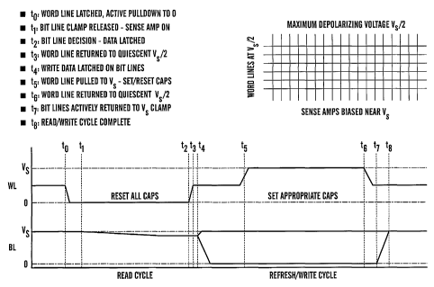
5 Example 1: Three-level (Vs/2) switching ,protocol
In certain special cases, a simplified pulsing protocol may be used, where all
inactive word and bit lines are given the same potential, i.e. V;" = 0. In
that
case, the minimum voltage value attainable across non-addressed cells
becomes:
10 (4) V;; = V;;; = Vs/2
and at least three separate potentials are needed for managing the write and
read operations (i.e. ~o , cho+Vs/2, ~o+Vs; where coo is a reference
potential).
As was mentioned above, partial switching may represent a serious problem
15 at voltage levels of Vs/2, rendering three-Level protocols unacceptable.
However, the degree of partial switching at a given applied voltage depends
explicitly on the ferroelectric material in question. Referring to fig.l,
materials with a square shaped hysteresis curves shall in many applications
yield acceptable performance.
Recently, certain classes of ferroelectrics such as organic polymers have
received much attention as memory substances in advanced data storage
concepts. In addition to other attractive features, theses materials exhibit
hysteresis curves far more square shaped than those of the ceramic
ferroelectrics that have traditionally dominated developments in the field of
ferroelectric-based non-volatile memory devices. Thus, it has becorne
relevant to define pulsing protocols which can satisfy the requirements of
realistic and optimized electronic device designs. Following upon the partial
switching problems that discouraged development and exploitation of early
efforts based on three-level switching protocols, these aspects have received
very little attention, which the present invention sets out to remedy.
Now examples of preferred embodiments shall be given.
Figs. 4 and 5 illustrate some three-Level pulsing protocols according to the
present invention, comprising a complete read cycle and a refresh/write
AMENDED SHEET
I ~-VO-GVVG IVVU I VVGO
CA 02412169 2002-12-09
16
cycle. Only the pulse diagrams for the active word- and bit lines are shown.
The inactive word lines may be kept stable at Vs/2 throughout the read/write
cycle, as may the inactive bit fines. Alternatively,. the latter may during
the
read cycle each be connected with a separate sense amplifier, which would be
biased near the bit line voltage when the bit line clamp is released (full row
readout). In the diagrams shown in figs. 4 and 5, the time markers are as
follows:
to : Word line latched, active pulldown to 0 (fig.4) or pullup to Vs
(fig. 5)
t1 : Bit line clamp released - sense amplifier ON
t2 : Bit line decision - data latched
t3 : Word line returned to quiescent Vs/2
t4 : Write data latched on bit lines
is : Word line pulled to Vs (fig. 4) or zero (fig. 5) - set/reset
capacitors
t6 : Word line returned to quiescent VS/2
t7 : Bit lines actively returned to Vs (fig. 4) or zero (fig. 5) clamp
t8 : Read/write cycle complete
The read cycle investigates the state of the polarization of the addressed
cell.
Depending on the polarization direction, the read operation may leave the
polarization unchanged, or it may reverse the polarization direction
(destructive read). In the latter case, the information must be refreshed if
it is
desired avoid loss of stored data. This implies that the polarization must be
driven in the opposite direction of the read operation in an appropriate cell
(not necessarily the one that was read) somewhere in the matrix. This is
achieved by the part of the protocol dedicated to refresh/write, as shown. The
two branches in the bit line voltage protocol correspond to the cases where
the polarization is left unchanged and reversed, respectively. An isolated
write operation is trivially achieved by omitting the preceding read
operation.
As shown in figs. 4 and 5, it is clear that non-addressed cells shall not
receive voltages exceeding 1/z of the nominal switching voltage, neither
AMENDED SHEET
IvvV Ivvtv,
I J-V V-tV Vt
CA 02412169 2002-12-09
17
during reading or refresh/writing periods. In addition, one notes that there
are
included event delays in the pulsing sequence to facilitate transient ring-
down and latching of data. Depending on how the memory device is to be
operated, the bit line potential m the quiescent state (i.e. between
read/refresh/write cycles) may be chosen to match that of the bit line at the
start of the read cycle (cf. figs. 4 and 5) or it may match the quiescent
potential of the word line (not shown here). In the former case, appropriate
when cycling is intense and at high speed, charging currents at the start of
the
read cycle are minimized. In the latter case, long-term effects of an imposed
field in the cells (e.g. imprint) are avoided.
It should be clear that the examples shown in figs. 4 and 5 may be modified
(e.g. by concurrent shifting of all potentials, or by minor departures from
exact voltage levels in the three-level scheme shown) without departing from
the essential principles illustrated therein.
Example 2: Four-level (V~/3) switchin~protocol
As described above, by employing at least 4 different potential levels on the
word and bit lines, one can ensure that no non-addressed cell experiences a
voltage exceeding 1/3 of the nominal switching voltage. Figs. 6 and 7
illustrate two variants of a preferred scheme for reading as well as
refreshing/writing data, according to the present invention. Here, the time
markers are as follows:
to : Quiescent state; all word- and bit lines at 2VS/3 (fig. 6) or Vs/3
(fig. 7)
t, : Inactive bit lines adjusted from quiescent value to Vs/3 (fig. 6)
or 2VS/3 (fig. 7)
t2 : Addressed bit lines) adjusted to VS (fig. 6) or 0 (fig. 7). Time
delay from t, to t2 is arbitrary; zero or negative timings are
acceptable also
t3 : After a programmable read-set up delay, the addressed word line
is adjusted from quiescent potential to 0 V (fig. b) or Vs (fig. 7),
a voltage of magnitude VS between addressed word and
bit lines. Unaddressed word lines remain at 2Vs/3 (fig.6) or VS/3
(fig. 7)
AMENDED SHEET
1~'VV'GVVG IVVV 1 VVG(
CA 02412169 2002-12-09
I8
t4 : Addressed word line returned to quiescent potential after read
delay
is : All bit lines returned to quiescent potential
t6 : Read cycle now complete. All word- and bit lines in quiescent
state (2VS/3 in fig. 6; Vs/3 in fig. 7)
t~ : All inactive word lines adjusted from quiescent to Vs/3 (fig. 6)
or 2Vs/3 (fig. 7)
t8 : Addressed bit lines) to be written to logic state "1" are
adjusted to 0 V or are left at quiescent potential to remain in
logic "0". (fig. 6) Addressed bit lines) to be written to logic
state "0" are adjusted to Vs or are left at quiescent potential to
remain in logic "1" {fig. 7)
tg : Addressed word line is adjusted to Vs (fig. 6) or 0 (fig. '7),
introducing a voltage of magnitude VS across addressed cells)
too : Addressed bit lines) returned to quiescent 2Vs/3 (fig. 6) or Vs/3
(fig. 7) after write delay
t~ ~ : All word lines returned to quiescent potential
t,2 : Write cycle complete. All word- and bit lines in quiescent
Apart from the increased voltage level complexity, the basic features are
similar to those referred above in connection with the three level schemes.
Now, however, no non-addressed cell is exposed to a voltage exceeding Vs/3
in the course of a complete read/write cycle, which shall cause only minor
partial switching in most ferroelectric materials of relevance here. Again,
several variants on a common theme are possible. Thus, figs. 6 and 7 show a
return to zero applied voltage across all cells in the quiescent state (cf.
the
above discussion under the three-level switching protocol), which
corresponds to word and bit line potentials of 2Vs /3 or VS /3, whereas other
potential levels on the word- and bit lines are possible in the quiescent
state
that either yield zero voltages across the cells or voltages of absolute value
c CVs' /3. Such variants shall be assumed obvious to the skilled person and
shall not be pursued in further detail here.
AMENDED SHEET
o-«~~ Nuu~uu~~
CA 02412169 2002-12-09
19
The timing diagrams in figs. 6 and 7 are equivalent in principle, one being an
"inverted" version of the other. In practice, however, one may be preferred
over the other. Thus, the scheme shown in fig.6, implies a voltage at the
sense
amplifier input during the read cycle near Vs . In the scheme of fig.7,
however, the voltage is near zero. This may permit the use of low voltage
components with a single high voltage pass transistor per bit line.
Example 3: Five-level VS/3~switching_protocol
A class of seemingly more complex, but in certain respects more simply
implemented pulsing protocols involve the application of five different
potential levels to the word- and bit lines during a complete read/write
cycle.
Explicit examples of two preferred embodiments are shown in figs. 8 and 9.
The time markers are as follows:
to : Quiescent state: all word- and bit lines at 2Vs/3 (fig. 8) or Vs/3
(fig. 9)
t1 : Inactive bit lines adjusted from quiescent value to Vs/3 (fig. 8)
or 2VS/3 (fig. 9)
t2 : Addressed bit lines) adjusted to Vs (fig. 8) or 0 (fig. 9). Time
delay from t, to tz is arbitrary; zero or negative timings are
acceptable also
t3 : After a programmable read-set up delay, the addressed word line
is adjusted from quiescent potential to OV (fig. 8) or 4Vs/3
(fig. 9), inducing a voltage of magnitude Vs between addressed
word and bit lines. Unaddressed word lines remain at 2Vs/3
(fig. 8) or Vs/3 (fig. 9)
t4 : Addressed word line returned to quiescent potential after read
delay
t5 : All bit tines returned to quiescent potential
t6 : Read cycle now complete. All word and bit lines in quiescent
state (2Vs/3 in fig. 8; VS/3 in fig. 9)
t~ : Inactive bit lines adjusted from quiescent to VS (fig.8) or Vs/3
(fig. 9)
AMENDED SHEET
1 ~-uo-GUUG IVVU I UULi:
CA 02412169 2002-12-09
t8 : Addressed bit lines) to be written to the "1" state are adjusted
to VS/3, while those that shall remain in state"0" are adjusted to
Vs {fig. 8); addressed bit lines) to be written to the "0" state are
adjusted to Vs/3, while those that shall remain in state"1" are
S adjusted to Vs (fig. 9)
t9 : Addressed word line is adjusted to 4Vs/3 (fig. 8) or 0 (fig. 9),
introducing a voltage of magnitude Vs across addressed cel!(s).
Non-addressed word lines remain at 2Vs/3
t,o : Addressed word lines returned to quiescent potential after write
10 delay
t~, : All bit lines returned to quiescent potential
t~Z : Write cycle complete. All word and bit lines in quiescent
Here, a fifth voltage level, V~~, is involved. It is typically of magnitude
4Vs/3, and is applied to the active word line during the reading (fig. 9) or
IS refresh/write (fig. 8) cycle. One notes that while the four-level schemes
in
figs. 6 and 7 require all word and bit lines to be driven at four levels in
the
course of the complete read/write cycle, the five-level schemes in figs. 8 and
9 require only three separate voltage levels to be applied to the word lines
and three separate but not identical voltage levels to be applied to the bit
20 lines. This provides opportunities for optimization and simplification of
the
driving and sensing electronics supporting the device. Further simplification
can be realized by choosing 4V$/3 = V~~ close to the power supply voltage.
Example 4: Switching protocols involving~pre-charging of non-addressed
cells on active bit lines
2S So far, primary focus has been on avoiding partial switching of non-
addressed cells. However, it is also desirable to design switching protocols
that simultaneously minimize the effect of parasitic current flows within the
memory matrix during the read cycle:
In memory matrices based on passive matrix addressing, the area data storage
density is maximized by using matrices that are as large as possible. This
implies that each matrix should contain the largest possible number of
crossing points between word and bit lines, and any given bit line must
consequently cross a large number of word lines. When a given word and bit
AMENDED SHEET
1.'7'VU'GVVL IVVV 1 VVGL
CA 02412169 2002-12-09
21
line crossing is selected, the large number of non-selected crossing points
between the bit line and all of the non-selected crossing word lines
constitute
a correspondingly large number of parasitic current leakage paths (capacitive,
inductive, ohmic) which may add up to slow down the device and reduce the
contrast ratio of as-read logic "1 "s and "0"s.
One method of reducing the effect of parasitic currents on the determination
of logic states is to pre-charge the non-addressed cells on the active bit
line
to a level corresponding to that which would be approached during the
reading of the active cell. This procedure is implicit in the voltage
protocols
shown in figs. 6-9. At time point 2, i.e. prior to applying the read voltage
step
to the active word line {at time point 3 in the figures) the active bit line
voltage is shifted to its read cycle value, creating a voltage bias between
the
active bit line and all word lines. This initiates the spurious current flows
in
all the non-active cells on the active bit line. These currents are typically
transient, reflecting polarization phenomena in the cells, and die out or are
greatly diminished after a short time. Thus, by making the time gap between
time points 2 and 3 sufficiently long, the spurious current contributions to
the
switching currents sensed during the reading cycle are greatly diminished.
Certain limitations adhere to this scheme: if the time gap between time points
2 and 3 becomes very long, it has obvious implications on the data access
speed and overall read cycle time. Additionally, the cumulative effect of
repeated cycling with long pre-charging times may be to cause partial
switching and imprint, which was sought avoided by having zero voltage
across all cells in the quiescent state.
The voltage protocol diagrams in figs. 6-13 do not show the sense amplifier
timing, which may vary from case to case, depending upon the dynamics of
the polarization switching and spurious current response in the addre$sed and
in the non-addressed cells. The sense amplifiers must be activated after time
point 2 to avoid the spurious current transient from the non-addressed cells,
and not much later than time point 3 in order to capture any polarization
reversal current in active cells that are switched by the read cycle.
One notes that by advancing the time point 2 well ahead of time point 3, not
only the inactive cells on the active bit line are subjected to an early
voltage
bias of magnitude ~ Vs~3 ~, but also the active cell. Thus, some of the
switching charge in the active cell is drained away before the sense amplifier
AMENDED SHEET
~ vvv i vvm
W J VVLVVL..
CA 02412169 2002-12-09
22
has been connected. The magnitude of this effect, which is undesirable since
it reduces the read signal, depends on the polarization characteristics of the
memory material in the cells and may range from negligible to significant. In
the latter case, one may implement a slight modification of the voltage
protocol by introducing a voltage shift on the inactive word lines as
illustrated in f gs. 10-13. The leading edge of the shift occurs at time point
0,
and the trailing edge coincides with the leading edge of the active bit line
voltage shift at time point 2. By precisely controlling the trailing and
leading
edge shifts at time point 2, the voltage across the non-addressed cells on the
I0 active bit line shall rise from zero to a magnitude ~ Vs/3 ~ at time point
0 and
remain unchanged at this value until time point 5, i.e. after completion of
the
read cycle. The time point 2 may now be optimized for the readout process in
the active cell, without limitations relating to driving the pre-charge
transient
in the non-addressed cells. As can be seen from figs. 10-13, the voltage
across non-addressed cells is always maintained at less than a magnitude
~ Vs/3 ~ in these modified schemes, but 4 voltage levels are now involved on
the word lines in the five-level protocols, compared to three levels
previously.
Example 5: Switching_protocols involvin, a reference pre-read cycle
Another scheme for circumventing or alleviating the problems relating to
parasitic currents in non-addressed cells on active bit lines shall now be
described.
For concreteness, refer to, e.g. the four-level timing diagram shown in fig.
6.
The pre-charge scheme described in the above paragraphs implies that the
active bit line has been shifted to its read cycle value at time point 2, and
ensuing parasitic currents have been significantly reduced by the time the
active word line is switched at time point 3. The logic state in the addressed
cell is determined by the sense amplifier which records the charge flowing to
the bit line during a defined time interval that starts near the time point 3
and
stops before the time point 4.
Ideally, such pre-charge schemes shall enable detection of the charge flowing
in response to the shifting of the active word line at time point 3, without
interference from parasitic currents through cells at inactive word lines. In
practice, the parasitic currents may die down slowly and/or have an ohmic
(i.e. non-transitory) component such that some parasitic charge is captured by
AMENDED SHEET
n vvv ~ vvw
CA 02412169 2002-12-09
23
the sense amplifier. Although the magnitude of the parasitic current
component flowing through each non-addressed cell on the active bit line
may be small, the currents from hundreds or thousands of non-addressed cells
on the active bit line may add up to become very significant, corrupting the
readout results.
Assuming stable and predictable conditions, such a parasitic contribution
may in principle be removed by subtracting a fixed amount of charge from
that recorded by the sense amplifier during the reading cycle. In many
instances, however, the magnitude and variability of the parasitic
contribution makes this inappropriate. Thus, in addition to the manufacturing
tolerances for the device, the fatigue and imprint history may vary within
wide limits between different cells in the same memory device and even on
the same bit Line, and the parasitic current may depend strongly upon the
device temperature at the time of read-out. In addition, the parasitic current
associated with a given non-addressed cell on the active bit line may depend
on which logic state it is in. In that case the cumulative parasitic current
from
all non-addressed cells on the active bit line shall depend on the set of data
stored in those cells, which defies prediction.
In order to obtain a true measure of the cumulative parasitic currents in
connection with a given read-out event, one may implement a pre-read
reference cycle as exemplified in fig. l4.
The pre-read cycle immediately precedes the read-out cycle and differs from
the latter in only one respect, namely that the active word line is not
shifted
at all. The sense amplifier is activated in precisely the same time slot
relative
to the bit line voltage shifts as is the case in the subsequent read cycle.
Thus,
the cumulative charge detected during the pre-read cycle shall correspond
very closely to the parasitic current contributions captured during the read
cycle, including contributions from the active cell. The detected charge from
the pre-read cycle is stored and subtracted from that recorded during the read
cycle, yielding the desired net charge from the switching or non-switching
transient in the active cell.
Clearly, the effects of fatigue, imprint, temperature and logic states are
automatically taken care of by this referencing scheme. An important
prerequisite is that the pre-read cycle must not materially alter the
parasitic
current levels in the read cycle. Thus, the delay between time points P6 and 0
AMENDED SHEET
CA 02412169 2002-12-09
24
(c~ fig. 14) must be sufficient for pre-read cycle transients to die down. In
certain cases, two or more successive pre-read cycles may be employed to
obtain a reproducible parasitic current response prior to the read cycle.
However, this increases complexity and total readout time.
Inspection of fig. 14 in conjunction with the four level pulse protocol shown
in fig. 6 shows how the pre-read reference cycle principle may be
implemented for the other pulse protocols covered by the present invention,
by trivial extension of the example given in the present instance.
Example 6: Switching protocols involvin~,offset volta~,es
Yet another scheme for circumventing or alleviating the problems relating to
parasitic currents in non-addressed cells on active bit lines shall now be
described.
According to Equation (2) above, the minimum disturbing voltage on non-
addressed cells is Vs/3 (cf. Equation (3)) and the preferred embodiments
described in conjunction with the four- and five-level switching protocols
were shown to achieve this. As will be discussed below, it may in certain
instances be preferable to deviate somewhat from this criterion.
Given that the memory cells exhibit certain characteristics regarding their
electrical impedance and switching properties, it is possible to achieve a low
parasitic current load on the bit line during read operations, while at the
same
time keeping disturbance of the non-addressed cells at a low level.
It is assumed that the selected cell is subjected to a voltage V; = Vs during
the period when the memory material in the cell undergoes polarization
switching. Thus,
(5) Vs = V;; + V;;; - V;,,
It is desired to lower the cumulative leakage current on the active bit line
which
flows through the non-addressed cells on that line. This can be achieved by
lowering the voltage across the non-addressed cells by an amount 8. Thus,
(6) V;;; ~ V;;; - 8
According to (5), this increment must be compensated by a corresponding
adjustment in the voltages across the remaining non-addressed cells:
~a - v;~ -~ V;; - V;~ + s
AMENDED SHEET
CA 02412169 2002-12-09
In a large matrix, the number of cells with inactive word and inactive bit
lines
(V;,,) greatly outnumber the cells with an active word line crossing an
inactive bit
line (V;;). To minimize the overall disturbance of non-addressed cells in the
matrix, one may therefore impose the requirement that V;,, shall not be
changed to
5 compensate for the reduction in V;;; , in which case one has:
Vii '~ Vii + s
Of course, this is not the only possible choice, but it shall be assumed
hereafter to
facilitate understanding of the basic principles involved.
Thus the Vs/3 protocol would be modified such that: V; = Vs, V;; = Vs/3 + s,
10 V;;; = Vs/3 - s, V;" _ -Vs/3. This can be achieved by, e.g. leaving the
potentials on
the active word and bit lines unchanged, while adding s to all inactive word
and
bit lines:
1) Vi = Vs '- ~activeBL ' ~activeWL: Active word line crossing active
bit line (the selected cell)
15 11) V;; = Vs/3 + s = (~;nactiveBL + S) ' ~activeWL~ Active word line
crossing inactive bit line
111) V;;; = Vg/3 - s = ~activeBL ' (~inactiveWL + s): Inactive word line
crossing active bit line
LV) V;v = -Vg/3 = (~;nactiveBL + s) - (~inactiveWL + S). Inactive word
20 line crossing inactive bit line
The magnitude of s must be selected with due consideration to two
conflicting requirements: On the one hand, it should be as large as possible
in
order to minimize parasitic current contributions to the active bit line. On
the
other hand, it should be as small as possible in order to minimize the
25 disturbance of non-addressed cells. In practice, a decision must be made
based on the specific conditions prevailing in each case.
Furthermore it is well-known to persons skilled in the art that the
electrically
polarizable materials used as the storage or memory medium in displays and
memories can have a non-linear voltage-current response characteristic
which may be exploited with advantage when implementing switching
protocols involving offset voltages. Such non-linear response characteristic
may however, also be dependent on the specific material and its treatment
AMENDED SHEET
CA 02412169 2002-12-09
26
and factors which in the present context may depend on the pulsing protocol
parameters actually used as well as design and scale factors. This implies
that
it will be impossible to generalize about a beneficial exploitation of
non-linear voltage-current response in non-addressed cells, but that any
specific embodiment involving this kind of response must be subject to the
heuristics as applicable in each case. However, any heuristics of this kind
shall be considered to lie outside the scope of the present application.
Example 7: Fuli row readout
An alternative route to reducing or eliminating the spurious current
contributions from non-addressed cells along active bit lines during readout
is illustrated in fig.l5. All word lines except the active one are clamped at
a
potential close to that at the sense amplifier input (defined as zero in
fig.l5).
For readout of data, the active word line is brought to the potential VREAD,
which causes currents to flow through the cells on the crossing bit lines. The
magnitudes of the currents depend on the polarization state in each cell and
are determined by the sense amplifiers, one for each bit line as shown.
This scheme provides several advantages:
- Voltages across all non-addressed cells are very close to zero, eliminating
leakage currents that may otherwise corrupt the readout from the addressed
cells.
- The readout voltage V,~AD may be chosen much higher than the coercive
voltage without incurring partial switching in non-addressed cells. This
allows for
film switching speeds approaching the intrinsic switching speed of the
polarizable
material in the cells.
- The scheme is compatible with large matrix arrays.
- The high degree of parallelism makes possible a large data readout rate.
Since the readout is destructive, it shall in many cases be necessary to write
data
back into the memory device. This can be achieved by one of the pulsing
schemes
described in the previous paragraphs. A different set of cells in the memory
device from those that were read may be chosen for refresh, e.g. in
conjunction
with caching.
Possible disadvantages of this scheme are largely related to the increased
demands
on the circuitry performing the driving and sensing functions. Thus, the
simultaneous switching of all cells on a long word line shall cause a large
current
AMENDED SHEET
CA 02412169 2002-12-09
27
surge on that line (implies a need for low source impedance in the driver
stage and
low impedance current paths. Also potential for cross-talk within the device).
Furthermore, in order to avoid loss of data a separate sense amplifier is
needed on
each bit line. With the highest possible density of cells in the passive
matrix, this
poses a crowding problem at the edge of the matrix where the sense amplifiers
are
connected.
The switching protocols described above make possible the controlled switching
of polarization direction of any given cell in a passive matrix arrangement,
without
subjecting non-addressed cells to disiz.irbing voltages that exceed ~Vs/3.
As described in the examples above, the pulsing protocols are directly
applicable
to the reading of logic states in memory cells that either experience no
polarization
switching during the read cycle, defined as being in e.g. a logic "0", or
switch the
direction of the polarization, correspondingly defined as being in a logic "1
".
Initialization of the memory could involve the writing of 0's in all cells,
which in
the case above would imply performing a read pulse cycle (destructive read).
Writing would then be achieved by applying the pulse sequence for changing the
polarization in those cells that shall store a logical "1" while leaving the
rest of the
cells unchanged. Subsequent reading of data from the memory would then require
a refresh cycle to be implemented in those cases where it is desired to retain
data
in the memory following the destructive read. The refresh protocol would
require a
complete read/refresh pulse sequence in cases where other cells are used for
renewed storage than those that were read destructively to provide the data.
On the
other hand, if the same cells are used, those cells that were read as logic
"0" can be
left unchanged and only those that contained a "1" need to be exposed to
polarization switching.
AMENDED SHEET