Note: Descriptions are shown in the official language in which they were submitted.
CA 02412514 2002-12-19
WO 02/00446 PCT/GBO1/02906
1
A SECURITY DEVICE
The invention relates to a security device, for
example for use on documents and articles of value such as
bank notes and the like to reduce the risk of
counterfeiting.
A common form of security device is an optically
variable device, such as a hologram or diffraction grating.
These devices are commonly formed as relief structures in
a substrate, which is then provided with a reflective
coating, for example a continuous or partial metallic layer
to enhance the replay of the device. The device is then
adhered to the article or document which is to be secured.
With the increased sophistication of counterfeiters,
it is important to develop known devices so as to enhance
their security.
Some examples of known security devices are described
in US-A-5815292, US-A-5742411, US-A-4662653 and EP-A-
0395410.
In accordance with the present invention, a security
device comprises a substrate formed with a surface relief
defining an optically variable effect generating structure;
and at least two different reflection enhancing materials
on, or on the same side of the substrate with respect to,
the surface relief, whereby the optically variable effect
can be viewed against a background defined by the
reflection enhancing materials.
We have devised a new type of security device which
has a number of distinct advantages over the conventional
technologies. For example, by using reflection enhancing
materials with distinctly differing appearances (such as
copper and aluminium) it is possible to form optically
variable images, such as holograms, which will have their
"rainbow" diffraction spectrum spatially modulated by the
reflective hue of the underlying metallic pattern, to
create a new and secure visual effect. These metallic
CA 02412514 2002-12-19
WO 02/00446 PCT/GBO1/02906
2
colours and replays are very difficult to match by dyeing
or colouring material layers.
In particular, the invention leads to a security
device which will, even to the untrained eye, have an
aesthetic, distinct, and novel appearance when compared
with a conventional device. This approach also presents a
very high technological barrier for the counterfeiter to
surmount and serves to distinguish the genuine hologram
from a counterfeit image even in the case where the
counterfeiter has managed to sufficiently reproduce the
holographic effect/microstructure either optically or by
mechanical replication.
Although the invention is primarily concerned with the
generation of holograms, the surface relief can more
generally define a diffraction grating, or even a coarser
form of microstructure, for example regular triangulated
features with sizes > 10 microns or randomised features
which change in a visually significant way, the specular
characteristics in certain areas.
In some examples, the reflection enhancing materials
define a common plane. Thus, the reflection enhancing
materials may be laid down side by side, or one reflection
enhancing material may be laid down in portions while the
other reflection enhancing material is provided fully over
the substrate and the one reflection enhancing material, so
filling the gaps between the one reflection enhancing
material.
In other examples, the reflection enhancing materials
are provided in different layers, either in contact with
one another or separated by one or more transparent
intermediate layers. This latter approach leads to further
advantages in that where these reflection enhancing layers
are metals, the intermediate layer or layers can comprise
a dielectric, one or both of the layers being formed as a
pattern defining a rf resonant circuit, which can be
remotely detected.
CA 02412514 2002-12-19
WO 02/00446 PCT/GBO1/02906
3
The device may also be verified by chemical or
physical analysis.
The contacting of dissimilar metals also causes
galvanic potentials to be established and these can be used
to sense the presence of the layer. The magnitude of the
potentials can be tailored by judicious choice of
materials.
When the reflection enhancing materials are laid down
in respective, different layers, the reflection enhancing
material in the layer furthest from the surface relief must
in general be visible through the layer containing the
first reflection enhancing material (unless this further
layer is covert). This can be achieved by using a
reflection enhancing material which is partially
transparent, for example a high refractive index layer such
as ZnS, or by providing the first reflective material in a
partial manner, for example partially demetallising the
layer to leave clear and opaque regions in defined
patterns, e.g. dots.
The reflection enhancing materials may also be laid
down in patterns defining indicia, graphic elements, logos,
crests, bar codes (1D and 2D) and the like which may or may
not be related to or registered with the optically variable
effect, such as a hologram, generated by the surface relief
structure.
Typically, these reflection enhancing materials will
comprise metals, such as aluminium and copper, but other
metals could also be used such as tin, nichrome, silver,
gold, nickel, stainless steel and also various alloys.
When, for example, the copper is applied over an aluminium
layer it provides protection from physical attack, copper
being more durable than aluminium, and can also act as an
electromagnetic shield should this property be required.
Alternatively, as mentioned above, other materials such as
high refractive index layers including ZnS could be used in
conjunction with semi-conductors, for example silicon or
CA 02412514 2002-12-19
WO 02/00446 PCT/GBO1/02906
4
germanium, and other optically distinctive inorganic and
organic films.
The reflection enhancing materials may be laid down in
a variety of ways, and in preferred examples are at least
in part in a predetermined pattern of for example dots or
lines. For example, if the first reflection enhancing
layer (e.g. aluminium) is formed with a fine array of
dots/lines (too small to be individually discerned by the
naked eye) then a continuous overlay of the second
reflection enhancing layer (e.g. copper) will create a
weighted two colour halftone or screen. By adjusting the
relative screen weights of the two metals a range of
colours/hues in the range aluminium-gold-bronze-copper
could be formed. Of course by macro patterning the screen
weight of the first layers (preferably in register with the
holographic design) to vary between 100% (solid Aluminium)
and 0% (solid copper) patterned graded hues could be
formed.
Graded structures formed in this way will have a novel
attractive appearance with the copper toning down the
sometimes overpowering brightness or lustre of aluminium
particularly when applied to more aesthetically traditional
areas such as banknotes. The backing layer could also
serve to increase the chemical durability and heat
resistance of the device.
In some cases, at least one of the reflection
enhancing materials will extend to an edge of the
substrate. However, in the preferred approach, there is no
reflective material in a border region extending along an
edge of the substrate. This is particularly useful in
embodiments which constitute transfer foils and the like so
as to minimise problems such as edge flashing and minor
mis-registration or alignment of hot stamping dies.
A further development would be to fabricate the fine
screening of aluminium dots/lines such that their spacing
or pitch matched that of a lenticular prism or microlens
array which functions as the decoder. Therefore when the
CA 02412514 2002-12-19
WO 02/00446 PCT/GBO1/02906
lenticular array is placed over the bimetallic hologram,
striking moire effects will be observed - these effects
being orientation sensitive. This effect could be used to
reveal clear silver/copper colour shifts in selected areas.
5 This could be taken one step further and used to
incorporate covert information (generically and rather
loosely referred to within the industry as scambled indicia
features) within the screened/metallisations. This is done
by slightly changing the spacing or orientation of the
dots/Iines, within the localised regions that define the
covert pattern (which could be alphanumeric characters,
graphical features etc.). The level of change being
sufficiently small that the localised covert pattern cannot
be picked out by the naked eye however when the periodicity
matched decoder is placed over the hologram then the covert
pattern is clearly revealed. This approach has been used
for some time with conventionally printed structures, for
example as discussed in patent WO 97/20298 (i.e. scrambled
indicia). Its use with metallised layers is, however,
novel.
The presence of a line structure of alternating
materials, which have dissimilar radiation absorption
characteristics, will also provide effects, which could be
used to encode security indicia.
Although the use of two reflection enhancing materials
has been described, the invention is applicable to three or
more such materials.
In an important embodiment, a further image may be
provided using ink or the like between the surface relief
and an adjacent one of the reflection enhancing materials.
This is described in much more detail in WO-A-91/06925
incorporated herein by reference.
It will be understood that the security device can be
used with a variety of documents and articles, but is
particularly designed for use with documents of value,
including visas, passports, licences, cheques, identity
cards, plastic cards, banknotes, tickets, bonds, share
CA 02412514 2002-12-19
WO 02/00446 PCT/GBO1/02906
6
certificates, vouchers, passes, permits, electrostatic
photocopies, electrostatic laser printed materials, brand
authentication labels, serial numbering slips, quality
control certificates, bills of lading and other shipping
documentation, legal documents and tamper evident labels.
The device can also be used on/in features such as
threads, tear tapes, self adhesive foils, hot stamping
foils or other Brand Protection applications such as shrink
sleeves.
The device can be used to introduce barcodes or
magnetic reading indicia amongst other machine readable
type features. Tt could also be used with tamper evident
features.
Some examples of security devices according to the
invention will now be described with reference to the
accompanying drawings in which:
Figure 1 is a schematic, cross-section through one
example of the device, not to scale;
Figure 2 is a schematic, cross-section through a
second example;
Figure 3 is a plan view of an example based on Figure
2;
Figure 4 is a plan of an example including a covert
feature;
Figure 5 is a view similar to Figure 1 but
illustrating a further example;
Figure 6 illustrates the appearance of a bar code;
and,
Figure 7 is a plan view of a still further example.
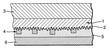
The device shown in Figure 1 comprises a lacquer or
polymeric substrate 1 having a typical thickness of 1-5~m,
into one surface of which has been embossed an optically
variable microstructure 2. The substrate 1 is supported on
a carrier layer 3, for example polypropylene or PET with a
typical thickness of 10-50~,m and the interface between the
two layers has been treated, for example, with corona
CA 02412514 2002-12-19
WO 02/00446 PCT/GBO1/02906
7
discharge or wax release, so that they can be detached in
a controllable way.
The surface relief 2 is vacuum coated with an
aluminium layer 4, typically 20-100nm thick, which is then
partially demetallised in a designed pattern to render it
partially transparent. The aluminium layer is then coated
with a thicker layer of copper 5, typically 40-200nm, and
finally a 0.5-20um thick hot melt adhesive layer 6 (or a
pressure sensitive adhesive for cold transfer) is provided
on the copper layer 5.
In use, the device shown in Figure 1 with a hot melt
adhesive 6 is applied to a document to be secured, and a
hot stamping die is brought into engagement with the
carrier 3, causing the adhesive 6 to be activated so as to
adhere the device to the document, following which the
carrier 3 is peeled away.
When the device is viewed through the lacquer layer 1,
the viewer will see the hologram generated by the surface
relief 2 in a conventional manner. However, that hologram
will be viewed against a coloured background having a very
distinctive appearance.
The example just described is in the form of a
transfer structure but the invention is also applicable to
hand applied labels. In that context, the carrier layer 3
would be omitted while the adhesive 6 would be a pressure
sensitive adhesive.
As mentioned above, a variety of different types of
device can be created:
Figure 2 illustrates an example in which the
components having the same form as in Figure 1 are given
the same reference numerals. The difference in this case
is that a dielectric layer 7 has been inserted between the
demetallised aluminium 4 and the copper layer 5. Typical
dielectrics include 200nm thick zirconium dioxide or zinc
sulphide. Alternatively, a semiconductor layer such as
50nm thick silicon could be used. The dielectric will be
transparent so that on viewing the device, the hologram
CA 02412514 2002-12-19
WO 02/00446 PCT/GBO1/02906
8
generated by the surface relief 2 can be seen against the
background defined by the aluminium layer 4 and the copper
layer 5. However, the device shown in Figure 2 has the
additional property that it can be detected electronically
by virtue of the capacitance generated between the two
metal layers 4, 5 . This will have a distinctive "signature"
allowing the device to be identified.
In a further alternative (not shown) the copper layer
5 could be patterned to define a rf resonant circuit, again
for electronic verification. Organic polymer coatings or
films could be interposed between the demet aluminium 4 and
the copper layer 5. These could be tinted, and/or contain
fluorescent materials as more fully described in EP-A-
0497837.
Figure 3 illustrates the appearance of a device
constructed similar to Figure 2, the darkest areas
corresponding to 100% copper and the lightest areas 100%
aluminium. A wide variety of densities is used to vary the
colours.
Figure 4 illustrates a device using copper and
aluminium and also including a covert feature 40 defining
indicia "IN" and formed by using different line patterns.
This could be viewed using a suitably formed. line or dot
screen.
Figure 5 illustrates a further example which has the
same constructions as shown in Figure 1 except with the
addition of ink images schematically indicated at 10 which
have been printed onto the surface relief 2. Typically,
these ink images will be in the form of security indica and
may have been provided using any known ink and as more
fully described and explained in WO-A-91/06925.
An important form of image produced by the reflective
layers 4, 5 is a bar code. An example of a bar code is
shown in Figure 6. The dark lines 12 are formed using
copper while the intermediate "white" lines 14 are formed
using aluminium. The feature is viewed under blue light
when copper appears black and aluminium appears white.
CA 02412514 2002-12-19
WO 02/00446 PCT/GBO1/02906
9
In the embodiments described so far, the aluminium
layer 4 is provided in a discontinuous manner while the
copper layer 5 is generally continuous although could be
discontinuous also. This means that the perimeter of the
security device will be defined by metal and thus the shape
of the device will be formed by the shape of the
blocking/hot stamping die (in the case of hot transfer
foils) or die-cutting head (in the case of hand applied
labels). However, much more intricately patterned metallic
shapes or regions can be achieved by utilizing the various
print based methods for achieving selective patterning of
the metal layers) or selective removal of the metal
layer(s). In particular, the use also of a discontinuous.
copper layer 5 is particularly important.
In a further embodiment particularly useful from a
manufacturing point of view, there will be no metal present
(copper or aluminium) within a border region of the device,
for example within say 1mm of the perimeter/edge of the
substrate. This facilitates effective transfer of images
defined by intricately patterned regions of metal and
minimises various problems as described above.
An example of this further embodiment is shown in
Figure 7. A first reflection enhancing layer is visible in
a region 40 while a second reflection enhancing layer is
visible in a region 41. A border region 42 is transparent
and def fined by uncoated areas of the substrate I which have
been transferred or applied to the final substrate 43.
In the preferred implementation of this embodiment of
Figure 7, the first reflection enhancing layer in the
region 40 is aluminium and the second reflection enhancing
layer in the region 41 is copper or a high copper-content
alloy.
Techniques for demetallising aluminium are well known
in the art (see, for example, US5044707, US5142383,
US5128779, US5145212), and normally involve the chemical
etching of the deposits using sodium hydroxide solutions.
This approach does not work well on copper-based alloys.
CA 02412514 2002-12-19
WO 02/00446 PCT/GBO1/02906
A variety of demetallisation processes may be used for
patterning copper layers, as follows.
The copper layer may be chemically etched using acid
solutions such as:
5 Hydrochloric acid 50ov
Ferric chloride (40° Baume) 50ov
(Room temperature)
Or
Sulphuric acid (66° Baume) 5-10%v
Ferrous sulphate 100g/litre
(40-60°C)
Other etchants may also be used such as nitric acid
but generally the above systems are the most convenient to
work with.
As with the techniques used for demetallising
aluminium layers, the etching may be carried out by
directly printing the etchant onto the surface, or
preferably by printing an etchant resistant masking layer
and then either immersing the web or spraying the etchants
over its surface.
The areas where copper is not required may be
precoated with mask composed of a solvent (e. g. water,
alcohol) soluble material and then copper coated. In the
latter case subsequent immersion in the appropriate solvent
then causes the precoat or mask to dissolve and the copper
on top of it to be dislodged. This approach has the
advantage that non-corrosive materials may be used.
An alternative (but functionally inferior) approach is
to print an opaque layer of (preferably white pigmented)
ink onto the microstructure either prior to the first or
the second reflection enhancing layer coating processes.
In this case area 42 in Figure 5 is no longer a transparent
area since the embossing layer has now been coated with an
opaque ink.