Note: Descriptions are shown in the official language in which they were submitted.
CA 02412977 2002-12-13
WO 01/96847 PCT/USO1/18846
-1-
Nanostructure-Based High Energy Capacity Material
STATEMENT REGARDING FEDERALLY SPONSORED
RESEARCH OR DEVELOPMENT
At least some aspects of this invention were made with Government support
under
contract no. N00014-98-1-0597. The Government may have certain rights in this
invention.
BACKGROUND OF THE INVENTION
In the description that follows references are made to certain compounds,
devices
and methods. These references should not necessarily be construed as an
admission that
such compounds, devices and methods qualify as prior art under the applicable
statutory
provisions.
With the increasing importance of batteries for a wide variety of uses,
ranging from
portable electronics to power supply devices for spacecraft, there is a long-
felt need for new
materials with higher energy densities.
The energy density of a material can be quantified by measuring the amount of
electron-donating atoms that can reversibly react with the material. One way
of obtaining
such a measurement is by setting up an electrochemical cell. The cell
comprises a container
housing an electrolyte, one electrode made of the electron-donating material
(e.g. - an alkali
metal), another electrode made of the material whose capacity is being
measured (e.g. - a
silicon nanostructure-based material), and an electrical circuit connected to
the electrodes.
Atoms of the electron-donating material undergo an oxidation reaction to form
ions of the
donating material, and free electrons. These ions are absorbed by the opposite
electrode, and
the free electrons travel through the electrical circuit. Since the number of
electrons "given
away" by each atom of the electron-donating material is known, by measuring
the number of
electrons transferred through the electrical circuit, the number of ions
transferred to the
material being investigated can be determined. This quantity is the specific
capacity of the
material, and can be expressed as milliampere-hours per gram of the material.
For example,
the maximum specific (reversible) capacity of graphite to accept lithium is
reported to be
approximately 372mAh/g. Because one lithium ion is transferred to the graphite
electrode
CA 02412977 2002-12-13
WO 01/96847 PCT/USO1/18846
_2_
for every electron released, the specific capacity can be expressed in terms
of the
stoichiometry of the electrode material. For graphite, the saturation phase
can be
characterized as LiC6 with Li ions residing between the graphene layers. See,
for example,
(M. Winter et al., Insertion Electrode Materials for Rechargeable Lithium
Batteries,
Advanced Materials, Vol. 10, 10, "725-762",1998; and J.R. Dahn et al.,
Mechanisms for
Lithium Insertion in Carbonaceous Materials, Science, volume 270, October 27,
1995.
Lithium intercalated graphite and other carbonaceous materials are
commercially
used as electrodes for advanced Li-ion batteries. See, for example, M.S.
Whittingham,
editor, Recent Advances in rechargeable Li Batteries, Solid State Ionics,
volumes 3 and 4,
number 69, 1994; G. Pistoria, Lithium Batteries: New Materials, Development
and
Perspectives, ElsevieY, 1994. The energy capacities of these conventional
battery materials
are partially limited by the LiC6 Li saturation concentration in graphite
(equivalent to
372mAh/g).
In order to increase the capacities of electrode materials other carbon based-
materials
have attracted attention as potential electrode materials. Disordered carbon
(soft and hard
carbon) materials show reversible lithium storage capacities higher than that
obtained from
graphite (see, for example, J.R. Dahn et al., Mechanisms for Lithium Insertion
in
Carbonaceous Materials, Science, volume 270, October 27, 1995). Single wall
carbon
nanotube bundles have a large reversible Li storage capacity of 1000mAh/g, but
at a large
voltage hysteresis.
Lithium alloys have been investigated as possible anode materials for Li-based
batteries. Si and Ge are known to form Li-rich alloys with compositions up to
LizZSiS or
Li22Ge5. They have been investigated for application in high temperature
molten salt
batteries (see, for example, R.N. Seefurth and R.A. Sharma, Investigation of
lithium
utilization from a lithium-silicon electrode, J. Electrochem. Soc., Vol. 124,
No. 8, 1207-
1214, 1977). However, electrochemcial reaction of Li with Si or Ge is only
possible at high
temperatures (higher than 350°C).
Pyrolysis of carbon and silicon-containing precursors has yielded materials
with
enhanced Li storage capacity (500-600mAh/g) (see, e.g.-Carbonaceous materials
containing
silicon as anodes for lithium-ion cells, Mat. Res. Soc. Proc., Vol. 393, page
305-313, 1995).
CA 02412977 2002-12-13
WO 01/96847 PCT/USO1/18846
-3-
It would be desirable to develop other materials having improved energy
storage
capacities and energy transfer properties. There exists a long-felt, but so
far unfulfilled
need, for a material having such properties. There exists a need for a
material having
improved properties that make it useful in battery electrodes and other high
energy
applications.
SUMMARY OF THE INVENTION
These and other objects are attained according to the principles of the
present
invention.
One aspect of the present invention includes a material comprising a
nanostructure
that can reversibly react with foreign species. The material having a
reversible capacity of at
least 900mAh/g.
Another aspect of the present invention includes a material comprising silicon
rod or
wire-like nanostructures and intercalted lithium, the material having a
reversible capacity of
at least 900mAh/g.
A further aspect of the present invention includes a germanium-based material
comprising a germanium and germanium oxide nanostructure. The material having
a
reversible capacity of at least 1000mAh/g.
In another aspect of the present invention, an article comprising an
electrically
conductive substrate, and a film deposited on the substrate which comprises
any of the
above-described materials. The article may take the form of an electrode for a
battery.
BRIEF DESCRIPTION OF THE DRAWING FIGURES
Figure 1 is a transmission electron microscope (TEM) micrograph of silicon
nanostructures fabricated by a Iaser ablation method;
Figure 2 is a powder x-ray diffraction pattern of the silicon nanostructures
used to
store lithium.
Figure 3 is a Raman spectrum of the silicon nanostructures of the present
invention;
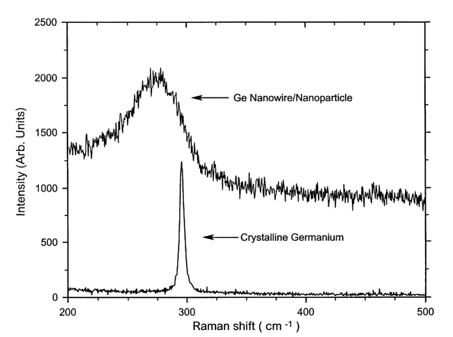
Figure 4 is a Raman spectrum of the germanium nanostructures of the present
invention;
CA 02412977 2002-12-13
WO 01/96847 PCT/USO1/18846
-4-
Figure 5 is a cross-sectional view of a nanostructure-coated substrate
according to the
present invention;
Figure 6 is an electrochemical cell incorporating an electrode material of the
present
invention;
Figure 7 is a graph showing the charge-discharge characteristics of a silicon
nanostructure material formed according to the principles of the present
invention;
Figure 8 shows the powder x-ray diffraction and Raman spectra collected from
the
electrode containing the silicon nanostructures at different stages of the
first discharge cycle;
and
Figure 9 is a graph showing the charge-discharge characteristics of a
germanium
nanostructure material formed according to the principles of the present
invention.
DETAILED DESCRIPTION OF PREFERRED EMBODIMENTS
A nanostructure-containing material can be formed by a number of techniques
familiar to those skilled in the art, such as laser ablation of a target
material, solution
synthesis or chemical vapor deposition.
While the particular technique used to produce nanostructures is not essential
to the
practice of the present invention, a brief description of the production of
such nanostructures
is given below for purposes of illustration.
Numerous nanostructure materials are contemplated by the present invention.
For
example, nanostructures formed from silicon (Si), germanium (Ge) and aluminum
(Al),
silicon oxide and germanium oxide are specifically contemplated.
According to typical laser ablation techniques, a target is placed within a
chamber.
Preferably, the target contains a suitable catalyst such as iron (Fe) or gold
(Au). The
chamber is evacuated and then filled with inert gasses such as argon. The
target is heated
and then ablated with a suitable energy source such as a pulsed laser.
As the target is ablated, nanostructure-containing material is recovered from
the
vaporized target.
CA 02412977 2002-12-13
WO 01/96847 PCT/USO1/18846
-S-
The nanostructure materials formed according to the technique described above
are
generally either cage-like spherical particles or rod/wire shaped objects
having nanometer-
scale dimensions.
For example, silicon nanostructures may comprise rod or wire-like shapes
having a
S diameter on the order of 1-SO nm and a length on the order of O.S-10 Vim.
Figure 1 is a TEM
micrograph of silicon nanostructures formed by a laser oblation technique.
Figure 2 is an x-
ray diffraction pattern of these silicon nanostructures. The FeSi2 peaks are
caused by the Fe
catalysts present in the Si target. Moreover, the outer surfaces of the
nanostructure objects
are typically covered by thin layers of silicon oxides.
Nanostructures apparently have higher surface to volume ratio than the bulk
material
from which they are derived or from other forms of the material such as
whiskers (see, for
example, R.S. Wagner and W.C. Ellis in Appl. Phys. Lett., Vol. 4, page 89,
1964 for the
synthesis of Si whiskers).
The nanostructures are more reactive and may also have a lower melting
temperature
1 S than the bulk materials. Therefore nanostructures formed of various
materials such as Si,
Ge, and Al exhibit increased reactivity and increased ability to reversibly
react with alkali
metals such as lithium.
For instance, Figure 3 illustrates another difference between bulk materials
and
nanostructures formed therefrom. As shown in Figure 3, the spectrum from bulk
crystalline
Si is compared with that of nanostructured Si. The characteristic Si sp3
stretching mode for
nanostructured Si is slightly down-shifted from that of bulk crystalline Si.
One suitable technique for producing silicon nanostructures is described in
A.M.
Morales and C.M. Lieber, A Laser Ablation Method for the Synthesis of C
.r~talline
Semiconductor Nanowires, Science, 279, 208-211, 1998; and Y.F. Zhang and et
al., Silicon
2S nanowires prepared by laser ablation at lugh temperature, Appl. Phys.
Lett., 72, 1S, 1835-
1837, 1998.
Similarly, Figure 4 illustrates the characteristic Ge sp3 stretching mode of
nanostructured Ge as being slightly down-shifted from that of the bulk
crystalline Si.
Nanostructured Ge was synthesized using the laser ablation method (e.g.-
Morales
and Lieber, Science vol. 279, 208-211, 1998). Target composed of Ge and Fe
(l0atm.%)
CA 02412977 2002-12-13
WO 01/96847 PCT/USO1/18846
-6-
was ablated by a pulsed Nd:YAG laser at 900C under a constant flow of argon.
Electron
microscopy measurements show that thus synthesized materials comprise both Ge
nanowires
with an average diameter of 5-30nm and micron in length, and nanoparticles
with the
average diameter of 1-50nm.
Another advantage of the nanostnzcture materials of the present invention is
that they
can be rather easily deposited as a film onto a substrate material. For
example, as illustrated
in Figure 5, a sample of purified nanostructure material can be solution-
deposited to form a
coating 12 on an appropriate substrate.
Nanostructure-based materials of the present invention unexpectedly possess
specific
lithium storage capacities that exceed those possessed by conventional carbon-
based
materials.
As described in the Background, in a testing electrochemical cell, the lithium
ions
travel from the lithium electrode to the nanostructure material electrode
during discharge.
The lithium ions are readily accepted into the large surface area of the
nanostnzcture
material. When a lithium ion is accepted into the nanostructure material
according to the
present invention a chemical reaction takes place, even at temperatures on the
order of
300°K and a distinct lithium-nanostructure material phase is formed,
thus forming an "alloy"
therewith. This reaction acts as a storage mechanism that enables the material
to hold a
charge (i.e.-in the form of lithium ions). As noted above, nanostructure
materials exhibit
increased reactivity. For example, while conventional macroscopic silicon must
be heated to
a temperature on the order of 400°C to react with lithium (see, for
example, R.N. Seefurth
and R.A. Sharma, Investigation of lithium utilization from a lithium-silicon
electrode, J.
ElectYOChem. Soc., Vol. 124, No. 8, 1207-1214, 1977; C.J. Wen and R.A.
Huggins,
Chemical diffusion in intermediate phase in the lithium-silicon s, stem, J: of
Solid State.
Chem., 37, 271-278 (1981).), the silicon nanostructure material of the present
invention
electrochemically reacts with lithium at room temperature or even lower.
The energy density, or ability of the silicon nanostructure material of the
present
invention to accept foreign species, such as alkali metals, and more
specifically lithium, was
measured by constructing a electrochemical cell, similar to that described in
the Background
CA 02412977 2002-12-13
WO 01/96847 PCT/USO1/18846
_7_
section above. An electrochemical cell incorporating the silicon nanostructure-
based
material of the present invention is schematically illustrated in Figure 6.
A cell was constructed with a lithium foil electrode 20 and a stainless steel
substrate
plate 10 having a nanostructure film 12 deposited thereon, as the second
electrode. A
polypropylene filter soaked with an electrolyte 22 was placed between the two
electrodes.
Electrical contacts were made by two stainless steel plungers 24, 26 pressed
against the
electrodes. A current source 28 is connected to the plungers. The cell was
then discharged
and charged.
The nanostructure-lithium materials of the present invention have
significantly
higher capacities than conventional materials. For example, the silicon
nanostructure-
lithium materials of the present invention have exhibited capacities of
1500mAh/g in the
first discharge cycle, reversible capacities on the order of at least 900mAh/g
to at least
approximately 1,OOOmAhlg and an irreversible capacity of less than SOOmAh/g.
Lithium
discharge occurs at essentially a constant voltage below 0.1 V. Most of the
lithium can be
removed from the nanostructured silicon electrode at below O.SV.
Figure 7 is a voltage-capacity plot for a fully lithiated silicon
nanostructure sample
that showed a total capacity of approximately 1300mAh/g. The reversible part,
defined as
the capacity displayed after the second discharge, is approximately800mAh/g.
The inset of
Figure 7 illustrates the capacity of the material versus the number of charge-
discharge
cycles. Figure 8 illustrates x-ray diffraction and Raman spectrum data
collected from
a Si nanostructure electrode at different stages of the first discharge cycle.
The x-ray and Raman intensities from the nanostructured Si decreases with
increasing Li concentration and vanished in the fully lithiated state(spectra
a, b and c). The
characteristic Si sp3 stretching mode re-appeared in the Raman spectrum in the
electrode at
the end of the first charge (spectrum d), indicating recovery of spa Si after
extraction of Li.
Inset shows the voltage versus capacity data from the same cell and the
integrated x-ray
intensity ratio of the Si (111) and FeSi2 peaks (FeSi2 is inert to Li and is
used as the internal
reference).
Figure 9 illustrates the second-cycle charge-discharge data from a sample
containing
nanostructured Ge and Ge oxide, after vacuum annealing at 150°C. The
data were collected
CA 02412977 2002-12-13
WO 01/96847 PCT/USO1/18846
_g-
under galvanostatic mode using SOmA/g rate at 300K. The reversible Li capacity
is
1500mAh/g (normalized with the total sample weight, the value will be higher
than the total
capacity is normalized with weight of nanostructured Ge, excluding the Fe
catalysts). A
distinct voltage step is present during both Li insertion and extraction.
Another important performance parameter is how the rate of charging and
discharging affects the capacity of the material. Some applications, such as
electrical
vehicles, require the electrode material to operate under high rate charging
and discharging
conditions. Generally, the capacity of the material decreases with an
increased rate. The
nanostructure-lithium material of the present invention exhibits high
capacities, even when
charged/discharged at high rates.
Yet another important performance parameter is the electrochemical potential
with
respect to Li. For example, lithium insertion into the current Si
nanostructure based material
occurs below O.1V and lithium extraction takes place mostly below O.SV. This
means that
the nanostructured silicon based materials can replace the current carbon
based negative
electrodes in the Li-Ion batteries without reduction in the cell voltage.
According to the present invention, it is also possible to further increase
the Li
storage capabilities of the nanostructure materials through addition
processing of the
material. For example, nanostructured Si samples from the same batch were
annealed at
different temperatures (200-900C) under SxlO-6torr vacuum. Their
charge/discharge
characteristics were measured under the same conditions as described above.
The total
discharge and reversible Li capacities were found to initially increase with
the annealing
temperature up to ~600C then decrease with further increase of the annealing
temperature.
Annealing is believed to remove chemical species on the surfaces of
nanostructured Si.
These chemical species and oxide coating can also be removed by other
processes such as
hydrogen plasma.
The excellent capacity of the nanostructure-based materials of the present
invention,
combined with their superb mechanical and electrical properties, and the ease
of forming
films, make them attractive electrode materials for high energy density
batteries (e.g.-high
energy density Li-ion batteries), batteries for high current rate
applications, and thin-film
batteries.
CA 02412977 2002-12-13
WO 01/96847 PCT/USO1/18846
-9-
Although the present invention has been described by reference to particular
embodiments, it is in no way limited thereby. To the contrary, modifications
and variants
will be apparent to those skilled in the art in the context of the following
claims.