Note: Descriptions are shown in the official language in which they were submitted.
CA 02413069 2002-12-16
WO 01/99208 PCT/USO1/19483
TITLE
THERMAL TREATMENT OF SOLUTION-PROCESSED ORGANIC
ELECTROACTIVE LAYER IN ORGANIC ELECTRONIC DEVICE
FIELD OF THE INVENTION
This invention related to organic electronic devices and their fabrication.
More particularly this invention relates to improvements in manufacturing such
devices which can lead to improved lifetimes and/or improved performance of
such devices.
BACKGROUND OF THE INVENTION
Organic electronic devices, such as light emitting devices, photodetecting
devices and photovoltaic cells, may be formed of a thin layer of electroactive
organic material sandwiched between two electrical contact layers.
Electroactive
organic materials are organic materials exhibiting electroluminescence,
photosensitivity, charge (hole or electron) transport and/or injection,
electrical
conductivity, and/or exciton blocking. The material may be semiconductive. At
least one of the electrical contact layers is transparent to light so that
light can pass
through the electrical contact layer to or from the electroactive organic
material
layer. Other devices with similar. structures include photoconductive cells,
photoresistive cells, photodiodes, photoswitches, transistors, capacitors,
resistors,
chemoresistive sensors (gaslvapor sensitive electronic noses, chemical and
biosensors), writing sensors, and electrochromic devices (smart windows).
Organic electroluminescent materials which emit light upon application of
electricity across the electrical contact layers include organic molecules
such as
anthracene, butadienes, coumarin derivatives, acridine, and stilbene
derivatives.
See, for example, U.S. Patent No. 4,356,429 to Tang. Semiconductive conjugated
polymers have also been used as electroluminescent materials. See, for
example,
Friend et al., U.S. Patent 5,247,190, Heeger et al., U.S. Patent No.
5,408,109, and
Nakano et al., Published European Patent Application 443 861. The
electroactive
organic materials can be tailored to provide emission at various wavelengths.
Light sensitive devices, such as photodetectors and photovoltaic cells, may
also use certain conjugated polymers and electro- and photo-luminescent
materials
to generate an electrical signal in response to radiant energy.
Electroluminescent
materials mixed with a charge trapping material, such as buckminsterfullerene
(C6p) and its derivatives, show such light sensitivity. See, for example, Yu,
Gang,
et al., "photovoltaic cells and photodetectors made with semiconductor
polymers:
Recent Progress", Conference 3939, Photonics West, San Jose, CA, January 22-
28, 2000.
CA 02413069 2002-12-16
WO 01/99208 PCT/USO1/19483
Organic electronic devices offer the advantages of flexibility, low cost and
ease of manufacture. (Id.) Their performance approaches and in some cases even
exceeds that of traditional photosensitive devices. (Id.) Organic electronic
devices
such as photoemitting, photodetecting and photovoltaic devices typically
include a
layer of charge injection/transport material adjacent to the
electroluminescent
organic material to facilitate charge transport (electron or hole transport)
and/or
gap matching of the electroactive organic material and an electrical contact.
Organic semiconducting material may also be used to form thin film
transistors. Transistors may now be fabricated completely from organic
materials.
1o Transistors of organic materials are less expensive than traditional
transistors and
may be used in low end applications where lower switching speeds maybe
acceptable and where it would be uneconomical to use traditional transistors.
See,
for example, Drury, C.J., et al., "Low-cost all-polymer integrated circuits",
Appl.
Phys. Lett., vol. ?3, No. 1, 6 July 1998, pp. 108-110. In addition, organic
transistors may be flexible, which would also be advantageous in certain
applications, such as to control light emitting diodes on a curved surface of
a
monitor. (Id.) Organic semiconducting materials include pentacene,
polythienylene vinylene, thiophene oligomers, benzothiophene dimers,
phthalocyanines and polyacetylenes. See, for example, U.S. Patent No.
5,981,970
2o to Dimitrakopoulos et al., U.S. Patent No. 5,625,199 to Bauntech, et al.,
U.S.
Patent No. 5,347,144 to Gamier, et al., and Klauck, Hagen et al., "Deposition:
Pentacene organic thin-film transistors and ICs," Solid State Technology, Vol.
43,
Issue 3, March 2, on pp. 63-75.
Electroactive organic materials may be applied to one of the electrical
contact layers or onto a portion of a transistor by solution processible
methods
such as spin-coating, casting or ink jet printing. Alternatively, these
materials
may be applied directly by vapor deposition processes, depending on the nature
of
the materials. In another alternate process an electroactive polymer precursor
may
be applied and converted to a polymer, typically by heat. Such alternate
methods
3o may be complex, slow, expensive, lack sufficient resolution and when
patterned
using the standard lithographic (wet development) techniques, expose the
device
to deleterious heat and chemical processes.
In many applications, especially in polymer emissive displays, arrays of
light-emitting diodes are assembled. In these applications there is typically
a unit
body of active polymer and the electrodes are patterned to provide the desired
plurality of pixels in the array. With arrays based on a unit body of active
polymer
and patterned electrodes there is a need to minimize interference or "cross
talk"
2
CA 02413069 2002-12-16
WO 01/99208 PCT/USO1/19483
among adjacent pixels. This need has also been addressed by varying the nature
of the contacts between the active polymer body and the electrodes.
The desire to improve operating life and efficiency is often seemingly at
cross purposes with the desire to minimize cross talk. High efficiency and
long
operating life are promoted by the use of high conductivity contacts with the
active material layer. Cross talk is minimized when the resistance between
adjacent pixels is high. Structures which favor high conductivity and thus
high
efficiency and long operating life are contrary to the conditions preferred
for low
cross talk.
1o In United States Patent No. 5,723,73 it is disclosed that it is
advantageous
to place a hole injection/transport material or buffer layer such as
conductive
polyaniline (PANI) between the hole-transport/injecting electrode and the
layer of
active material to increase diode efficiency and to lower the diode's turn on
voltage.
15 Polyaniline in the emeraldine salt form (PANI(ES)) as typically prepared
has intrinsically low electrical resistivity. However, for use in pixellated
displays,
the PANI(ES) or the like buffer layer needs to have a high electrical sheet
resistance, otherwise lateral conduction causes cross-talk between neighboring
pixels. The resulting inter-pixel current leakage significantly reduces the
power
20 efficiency and limits both the resolution and the clarity of the display.
United
States Patent No. 5,334,539 to Shinar et al describes the use of a 1-24 hour
annealing process for completed polyp-phenyleneacetylene) diode devices to
reduce the EL threshold voltage, i.e. the initial voltage at which the device
electroluminesces, by about 20% and to improve operating lifetime.
25 There is a continued need to improve the performance and lifetime of
electroactive organic devices.
SUMMARY OF THE INVENTION
The invention relates to an organic electronic device containing at least
one solution-processed organic electroactive material, wherein one or more of
the
30 at least one solution-processed organic electroactive material is heat-
treated.
The invention also relates to the use of heat treatment to improve the life
time and/or performance of an organic electronic device containing at least
one
layer of solution-processed organic electroactive material, by heat-treating
one or
more of such solution processed layers.
35 The invention further relates to a method of making an organic electronic
device containing a first electrode, a second electrode, and at least one
solution-
processed organic electroactive material between the first and second
electrodes,
wherein the method involves providing one or more of the at least one solution-
CA 02413069 2002-12-16
WO 01/99208 PCT/USO1/19483
processed organic electornic material on the first electrode and one or more
steps
of heat-treating one or more of the solution-processed organic electroactive
material before laying down the second electrode.
As used herein, the term "organic electroactive material" refers to any
organic material that exhibits the specified electroactivity, such as
electroluminescence, photosensitivity, charge transport and/or charge
injection,
electrical conductivity and exciton blocking. The term "solution-processed
organic electroactive material" refers to any organic electroactive material
that has
been incorporated in a suitable solvent during layer formation in electronic
device
to assembly. The term "charge" when used to refer to charge
injection/transport
refers to one or both of hole and electron transport/injection, depending upon
the
context. The term "photoactive" organic material refers to any organic
material
that exhibits the electroactivity of electroluminescence and/or
photosensitivity.
The terms "conductivity" and "bulk conductivity" are used interchangeably, the
value of which is provided in the unit of Siemens per centimeter (S/cm). In
addition, the terms "surface resistivity" and "sheet resistance" are used
interchangeably to refer to the resistance value that is a function of sheet
thickness
for a given material, the value of which is provided in the unit of ohm per
square
(ohm/sq). Also, the terms "bulk resistivity" and "electrical resistivity" are
used
2o interchangeably to refer to the resistivity that is a basic property of a
specific
materials (i.e., does not change with the dimension of the substance), the
value of
which provided in the unit of ohm-centimeter (ohm-cm). Electrical resistivity
value is the inverse value of conductivity.
DETAILED DESCRIPTION OF THE INVENTION
BRIEF DESCRIPTION OF THE DRAWINGS
This invention will be described with reference being made to the
drawings.
In these drawings,
Fig. 1 is a cross-sectional view of a representative solid state devices
3o embodying the invention (not-to-scale).
Fig. 2 is a graph which shows the stress induced degradation of a device
with PANI(ES) and its blend layer at 70°C.
Fig. 3 is a graph which shows the stress induced degradation of a device
from PANI(ES)-PAM blend with different heat treatment at 70°C.
Fig. 4 is a graph which shows the dependence of the conductivity of
PANI(ES)-PAM blends on baking time at 200°C.
Fig. 5 is a graph which shows the stress induced degradation of a device
with PANI(ES)-PAM blends baked at 200°C for different time at
70°C.
4
CA 02413069 2002-12-16
WO 01/99208 PCT/USO1/19483
Fig. 6 is a graph which shows the stress induced degradation of a device
with different PANI(ES)-PAM blends at 70°C.
Fig. 7 is a graph which shows the stress induced degradation of a device
with C-PPV layer baked at different temperatures.
DESCRIPTION OF THE PREFERRED EMBODIMENTS
This invention relates generally to the use of thermal treatment of at least
one solution-processed organic electroactive layers in an organic electronic
device
to provide significant improvements in stability and operating life.
DEVICE CONFIGURATION
to While the formulation of the invention is useful in non-pixelated as well
as
pixelated electronic devices, the advantages are especially applicable in
pixelated
devices.
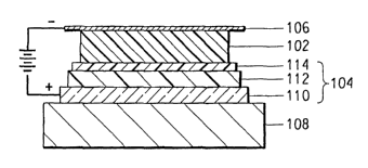
As shown in Fig. 1, each individual pixel of an organic electronic device of
the invention includes a cathode layer 106 and an anode layer 110 that is
deposited
on an optional substrate 108 (also known as the support) and electroactive
layers
102, 112 between the cathode 106 and anode 110. Adjacent to the anode 110 is a
hole injection/transport layer 112 (also known as the buffer layer). Between
the
hole injectionltransport layer 112 and the cathode 106 is the photoactive
layer 102.
The remainder of this description of preferred embodiments is organized
2o according to these various components. More specifically it contains the
following sections:
The Photoactive Layer (102)
The Anode (110)
The Buffer Layer ( 112)
The Cathode (106)
The Substrate (108)
Optional Components
Solution-Processed Organic Electroactive Layers
Fabrication Techniques
3o The Heat Treatment
Examples
The Photoactive Layer (102)
Depending upon the application of the electronic device, the photoactive
layer 102 can be a light-emitting layer that is activated by an applied
voltage (such
as in a light-emitting diode or light-emitting electrochemical cell), a layer
of
material that responds to radiant energy and generates a signal with or
without an
applied bias voltage (such as in a photodetector). Examples of photodetectors
include photoconductive cells, photoresistors, photoswitches,
phototransistors,
CA 02413069 2002-12-16
WO 01/99208 PCT/USO1/19483
and phototubes, and photovoltaic cells, as these terms are describe in Markus,
John, Electronics arad Nucleonics Dictionary, 470 and 476 (McGraw-Hill, Inc.
1966).
Where the electronic device is a light-emitting device, the photoactive
layer 102 will emit light when sufficient bias voltage is applied to the
electrical
contact layers. Suitable active light-emitting materials include organic
molecular
materials such asanthracene, butadienes, coumarin derivatives, acridine, and
stilbene derivatives, see, for example, Tang, U.S. Patent 4,356,429, Van Slyke
et al., U.S. Patent 4,539,507, the relevant portions of which are incorporated
1o herein by reference. Alternatively, such materials can be polymeric
materials such
as those described in Friend et al. (U.S. Patent 5,247,190), Heeger et al.
(U.S.
Patent 5,408,109), Nakano et al. (U.S. Patent 5,317,169), the relevant
portions of
which are incorporated herein by reference. The light-emitting materials may
be
dispersed in a matrix of another material, with and without additives, but
preferably form a layer alone. In preferred embodiments, the
electroluminescent
polymer comprises at least one conjugated polymer or a co-polymer which
contains segments of ~-conjugated moieties. Conjugated polymers are well
known in the art (see, e.g., Conjugated Polymers, J.-L. Bredas and R. Silbey
edt.,
Kluwer Academic Press, Dordrecht, 1991). Representative classes of materials
2o include, but are not limited to the following:
xxx
(i) poly(p-phenylene vinylene) and its derivatives substituted at various
positions on the phenylene moiety;
(ii) polyp-phenylene vinylene) and its derivatives substituted at various
positions on the vinylene moiety;
(iii) poly(arylene vinylene), where the arylene may be such moieties as
naphthalene, anthracene, furylene, thienylene, oxadiazole, and the like, or
one of
the moieties with functionalized substituents at various positions;
(iv) derivatives of poly(arylene vinylene), where the arylene may be as in
(iii) above, substituted at various positions on the arylene moiety;
(v) derivatives of poly(arylene vinylene), where the arylene may be as in
(iii) above, substituted at various positions on the vinylene moiety;
(vi) co-polymers of arylene vinylene oligomers with non-conjugated
oligomers, and derivatives of such polymers substituted at various positions
on the
arylene moieties, derivatives of such polymers substituted at various
positions on
the vinylene moieties, and derivatives of such polymers substituted at various
positions on the arylene and the vinylene moieties;
6
CA 02413069 2002-12-16
WO 01/99208 PCT/USO1/19483
(vii) polyp-phenylene) and its derivatives substituted at various positions
on the phenylene moiety, including ladder polymer derivatives such as poly(9,9-
dialkyl fluorene) and the like;
(viii) poly(arylenes) and their derivatives substituted at various positions
on the arylene moiety;
(ix) co-polymers of oligoarylenes with non-conjugated oligomers, and
derivatives of such polymers substituted at various positions on the arylene
moieties;
(x) polyquinoline and its derivatives;
(xi) co-polymers of polyquinoline with p-phenylene and moieties having
solubilizing function;
(xii) rigid rod polymers such as poly(p-phenylene-2,6-benzobisthiazole),
poly(p-phenylene-2,6-benzobisoxazole), poly(p-phenylene-2,6-benzimidazole),
and their derivatives; and the like.
More specifically, the light-emitting materials may include but are not
limited to poly(phenylenevinylene), PPV, and alkoxy derivatives of PPV, such
as
for example, poly(2-methoxy-5-(2'-ethyl-hexyloxy)-p-phenylenevinylene) or
"MEH-PPV" (United States Patent No. 5,189,136). BCHA-PPV is also an
attractive light-emitting material. (C. Zhang, et al, J. Electron. Mater., 22,
413
(1993)). PPPV is also suitable. (C. Zhang et al, Synth. Met., 62, 35 (1994)
and
references therein.) Luminescent conjugated polymer which are soluble in
common organic solvents are preferred since they enable relatively simple
device
fabrication [A. Heeger and D. Braun, U.S. Patent 5,408,109 and 5,869,350].
Even more preferred light-emitting polymers and copolymers are the
soluble PPV materials described in H. Becker et al., Adv. Mater. 12, 42 (2000)
and referred to herein as C-PPV's. Blends of these and other semi-conducting
polymers and copolymers which exhibit electroluminescence can be used.
Where the electronic device 100 is a photodetector, the photoactive layer 102
responds to radiant energy and produces a signal either with or without a
biased
3o voltage. Materials that respond to radiant energy and is capable of
generating a
signal with a biased voltage (such as in the case of a photoconductive cells,
photoresistors, photoswitches, phototransistors, phototubes) include, for
example,
many conjugated polymers and electroluminescent materials. Materials that
respond to radiant energy and are capable of generating a signal without a
biased
voltage (such as in the case of a photoconductive cell or a photovoltaic cell)
include materials that chemically react to light and thereby generate a
signal. Such
light-sensitive chemically reactive materials include for example, many
conjugated polymers and electro- and photo-luminescent materials. Specific
7
CA 02413069 2002-12-16
WO 01/99208 PCT/USO1/19483
examples include, but are not limited to, MEH-PPV ("Optocoupler made from
semiconducting polymers", G. Yu, K. Pakbaz, and A. J. Heeger, .Iourraal of
Electronic Materials, Vol. 23, pp 925-928 (1994); and MEH-PPV Composites
with CN-PPV ("Efficient Photodiodes from Interpenetrating Polymer Networks",
J. J. M. Halls et al. (Cambridge group) Nature Vol. 376, pp. 498-500, 1995). .
The electroactive organic materials can be tailored to provide emission at
various
wavelengths.
In some embodiments, the polymeric photoactive material or organic
molecular photoactive material is present in the photoactive layer 102 in .:
to admixture from 0% to 75% (w, basis overall mixture) of carrier organic
material
(polymeric or organic molecular). The criteria for the selection of the carnet
organic material are as follaws. The material should allow for the formation
of
mechanically coherent films, at low concentrations, and remain stable in
solvents
that are capable of dispersing, or dissolving the conjugated polymers for
forming
the film. Low concentrations of carrier materials are preferred in order to
minimize processing difficulties, i.e., excessively high viscosity or the
formation
of gross in homogeneities; however the concentration of the carrier should be
high
enough to allow for formation of coherent structures. Where the carrier is a
polymeric material, preferred carrier polymers are high molecular weight (M.W.
>
100,000) flexible chain polymers, such as polyethylene, isotactic
polypropylene,
polyethylene oxide, polystyrene, and the like. Under appropriate conditions,
which
can be readily determined by those skilled in the art, these macromolecular
materials enable the formation of coherent structures from a wide variety of
liquids, including water, acids, and numerous polar and non-polar organic
solvents. Films or sheets manufactured using these carrier polymers have
sufficient mechanical strength at polymer concentrations as low as 1 %, even
as
low as 0. 1 %, by volume to enable the coating and subsequent processing as
desired. Examples of such coherent structures are those comprised of polyvinyl
alcohol), polyethylene oxide), poly-para (phenylene terephthalate),
3o poly-para-benzamide, etc., and other suitable polymers. On the other hand,
if the
blending of the final polymer cannot proceed in a polar environment, non-polar
carrier structures are selected, such as those containing polyethylene,
polypropylene, poly(butadiene), and the like.
Typical film thicknesses of the photoactive layers range from a few
hundred I~ngstrom units (200 ~.) to several thousand angstrom units (10,000 ~)
(1 t~ngstrom unit = 10-8 cm). Although the photoactive layer film thicknesses
are
not critical, device performance can typically be improved by using thinner
films.
Preferred thickness are from 300 ~ to 5,000 ~.
CA 02413069 2002-12-16
WO 01/99208 PCT/USO1/19483
The Anode ( 110
In the device of the invention that contains a photoactive layer, one
electrode is transparent to enable light emission from the device or light
reception
by the device. Most commonly, the anode is the transparent electrode, although
the present invention can also be used in an embodiment where the cathode is
the
transparent electrode.
The anode 110 is preferably made of materials containing a metal, mixed
metal, alloy, metal oxide or mixed-metal oxide. Suitable metals include the
Group 11 metals, the metals in Groups 4, 5, and 6, and the Group 8-10
transition
1o metals. If the anode is to be light-transmitting, mixed-metal oxides of
Groups 12,
13 and 14 metals, such as indium-tin-oxide, are generally used. The IUPAC
numbering system is used throughout, where the groups from the Periodic Table
are numbered from left to right as 1-18 (CRC Handbook of Chemistry and
Physics, 81 St Edition, 2000). The anode 110 may also comprise an organic
material such as polyaniline as described in "Flexible light-emitting diodes
made
from soluble conducting polymer," Nature vol. 357, pp 477-479 (11 June 1992).
Typical inorganic materials which serve as anodes include metals such as
aluminum, silver, platinum, gold, palladium, tungsten, indium, copper, iron,
nickel, zinc, lead and the like; metal oxides such as lead oxide, tin oxide,
2o indiumltin-oxide and the like; graphite; doped inorganic semiconductors
such as
silicon, germanium, gallium arsenide, and the like. When metals such as
aluminum, silver, platinum, gold, palladium, tungsten, indium, copper, iron,
nickel, zinc, lead and the like are used, the anode layer must be sufficiently
thin to
be semi-transparent. Metal oxides such as indium/tin-oxide are typically at
least
semitransparent.
As used herein, the term "transparent" is defined to mean "capable of
transmitting at least about 25%, and preferably at least about 50%, of the
amount
of light of a particular wavelength of interest". Thus a material is
considered
"transparent" even if its ability to transmit light varies as a function of
wavelength
3o but does meet the 25% or 50% criteria at a given wavelength of interest. As
is
known to those working in the field of thin films, one can achieve
considerable
degrees of transparency with metals if the layers are thin enough, for example
in
the case of silver and gold below about 3001, and especially from about 20 t~.
to
about 250 ~ with silver having a relatively colorless (uniform) transmittance
and
gold tending to favor the transmission of yellow to red wavelengths.
The conductive metal-metal oxide mixtures can be transparent as well at
thicknesses up to as high as 2500 t~ in some cases. Preferably, the
thicknesses of
9
CA 02413069 2002-12-16
WO 01/99208 PCT/USO1/19483
metal-metal oxide (or dielectric) layers is from about 25 to about 1200 ~ when
transparency is desired.
This layer is conductive and should be low resistance: preferably less than
300 ohms/square and more preferably less than 100 ohms/square.
The Buffer Layer (112)
The buffer layer 112 facilitates hole injection/transport. The buffer layer
112 may include polyaniline (PANI) or an equivalent conjugated conductive
polymer such as polypyrole or polythiophene, most commonly in a blend with one
or more nonconductive polymers. Polyaniline is particularly useful. Most
commonly it is in the emeraldine salt (ES) form. Useful conductive
polyanilines
include the homopolymer and derivatives usually as blends with bulk polymers
(also known as host polymers). Examples of PANI are those disclosed in United
States Patent No. 5,232,631. The preferred PANI blend materials for this layer
have a bulk conductivity of from about 10-4 S/cm to 10-11 S/cm. More preferred
PANI blends have a bulk conductivity of from 10-5 S/crn to 10-& Slcm.
Suitable conductive materials that can be included in the buffer layer 112
include N,N'-diphenyl-N,N'-bis(3-methylphenyl)-[l,l'-biphenyl]-4,4'-diamine
(TPD) and bis[4-(N,N-diethylamino)-2-methylphenyl](4-methylphenyl)methane
- (MPMP), and hole injection/transport polymers such as polyvinylcarbazole
(PVK), (phenylmethyl)polysilane, poly(3,4-ethylenedioxythiophene) (PEDOT),
and polyaniline (PANI);electron and hole injection/transporting materials such
as
4,4'-N,N'-dicarbazole biphenyl (BCP); or light-emitting materials with good
electron and hole transport properties, such as chelated oxinoid compounds,
such
as tris(8-hydroxyquinolato)aluminum (Alq3).
When the terms "polyaniline" or PANI are used herein, they are used
generically to include substituted and unsubstituted materials, as well as any
accompanying dopants, particularly acidic materials, used to render the
polyaniline conductive.
3o In general, polyanilines are polymers and copolymers of film and fiber-
forming molecular weight derived from the polymerization of unsubstituted and
substituted anilines of the Formula I:
Formula I
NH2
~m 10
CA 02413069 2002-12-16
WO 01/99208 PCT/USO1/19483
wherein
n is an integer from 0 to 4;
m is an integer from 1 to 5 with the proviso that the sum of n and m is
equal to 5; and
R is independently selected so as to be the same or different at each
occurrence and is selected from the group consisting of alkyl, alkenyl,
alkoxy,
cycloalkyl, cycloalkenyl, alkanoyl, alkythio, aryloxy, alkylthioalkyl,
alkylaryl,
1o arylalkyl, amino, alkylamino, dialkylamino, aryl, alkylsulfinyl,
alkoxyalkyl,
alkylsulfonyl, arylthio, arylsulfinyl, alkoxycarbonyl, arylsulfonyl,
carboxylic acid,
halogen, cyano, or alkyl substituted with one or more sulfonic aid, carboxylic
acid,
halo, nitro, cyano or epoxy moieties; or carboxylic acid, halogen, nitro,
cyano, or
sulfonic acid moieties; or any two R groups together may form an alkylene or
15 alkenylene chain completing a 3, 4, 5, 6 or 7-membered aromatic or
alicyclic ring,
which ring may optionally include one or more divalent nitrogen, sulfur or
oxygen
atoms. Without intending to limit the scope of this invention, the size of the
various R groups ranges from about 1 carbon (in the case of alkyl) through 2
or
more carbons up through about 20 carbons with the total of n Rs being from
about
20 1 to about 40 carbons.
Illustrative of the polyanilines useful in the practice of this invention are
those of the Formula II to V:
(R~,
II ~ ~ NH ~ . ~ NH
L '-'
" c
Y z
or
11
CA 02413069 2002-12-16
WO 01/99208 PCT/USO1/19483
(R~n
III / . \ NH
I
(gym z
or
~~n
H
IV ~ / N ~ ~ N N
~~m ~ ~m
x Y
Z
or
~R~n
H
V \ / N ~ ~ N N
~m y
1111X
Z
wherein:
n, m and R are as described above except that m is reduced by 1 as a
hydrogen is replaced with a covalent bond in the polymerization and the sum of
n
1 o plus m equals 4;
y is an integer equal to or greater than 0;
x is an integer equal to or greater than 1, with the proviso that the sum of x
and y is greater than 1; and
z is an integer equal to or greater than 1.
15 The following listing of substituted and unsubstituted anilines are
illustrative of those which can be used to prepare polyanilines useful in the
practice of this invention.
12
CA 02413069 2002-12-16
WO 01/99208 PCT/USO1/19483
Aniline 2,5-Dimethylaniline
o-Toluidine 2,3-Dimethylaniline
rn-Toluidine 2,5-Dibutylaniline
o-Ethylaniline 2,5-Dimethoxyaniline
m-Ethylaniline Tetrahydronaphthylamine
o-Ethoxyaniline o-Cyanoaniline
m-Butylaniline 2-Thiomethylaniline
m-Hexylaniline 2,5-Dichloroaniline
m- Octylaniline 3-(n-Butanesulfonic acid)aniline
4-Bromoaniline
2-Bromoaniline
3-Bromoaniline 2,4-Dimethoxyaniline
3-Acetamidoaniline 4-Mercaptoaniline
4-Acetamidoaniline 4-Methylthioaniline
5-Chloro-2-methoxyaniline 3-Phenoxyaniline
5-Chloro-2-ethoxyaniline 4-Phenoxyaniline
Illustrative of useful R groups are alkyl, such as methyl, ethyl, octyl,
nonyl,
tert-butyl, neopentyl, isopropyl, sec-butyl, dodecyl and the like, alkenyl
such as
1-propenyl, 1-butenyl, 1-pentenyl, 1-hexenyl, 1-heptenyl, 1-octenyl and the
like;
alkoxy such as propoxy, butoxy, methoxy, isopropoxy, pentoxy, nonoxy, ethoxy,
octoxy, and the like, cycloalkenyl such as cyclohexenyl, cyclopentenyl and the
like; alkanoyl such as butanoyl, pentanoyl, octanoyl, ethanoyl, propanoyl and
the
like; alkylsulfinyl, alkysulfonyl, alkylthio, arylsulfonyl, arylsulfinyl, and
the like,
1 o suchas butylthio, neopentylthio, methylsulfinyl, benzylsulfinyl,
phenylsulfmyl,propylthio, octylthio, nonylsulfonyl, octylsulfonyl, methylthio,
isopropylthio, phenylsulfonyl, methylsulfonyl, nonylthio, phenylthio,
ethylthio,
benzylthio, phenethylthio, naphthylthio and the like; alkoxycarbonyl such as
methoxycarbonyl, ethoxycarbonyl, butoxycarbonyl and the like, cycloalkyl such
as
cyclohexyl, cyclopentyl, cyclooctyl, cycloheptyl and the like; alkoxyalkyl
such
asmethoxymethyl, ethoxymethyl, butoxymethyl, propoxyethyl, pentoxybutyl and
the like; aryloxyalkyl and aryloxyaryl such as phenoxyphenyl, phenoxymethylene
andthe like; and various substituted alkyl and aryl groups such as 1-
hydroxybutyl,
1-aminobutyl, 1-hydroxylpropyl, 1-hydyroxypentyl, 1-hydroxyoctyl,
1-hydroxyethyl, 2-nitroethyl, trifluoromethyl, 3,4-epoxybutyl, cyanomethyl,
3-chloropropyl, 4-nitrophenyl, 3-cyanophenyl, and the like; sulfonic
13
CA 02413069 2002-12-16
WO 01/99208 PCT/USO1/19483
acidterminated alkyl and aryl groups and carboxylic acid terminated alkyl and
aryl
groups such as ethylsulfonic acid, propylsulfonic acid, butylsulfonic
acid,phenylsulfonic acid, and the corresponding carboxylic acids.
Also illustrative of useful R groups are divalent moieties formed from any
two R groups such as moieties of the formula:
-(CHZ)-"*
wherein n* is an integer from about 3 to about 7, as for example -(CHa)_4,-
(CHZ)_3
l0 and -(CH2)_5, or such moieties which optionally include heteroatoms of
oxygen
and sulfur such as -CHzSCH2- and -CHZ-O-CHZ-. Exemplary of other useful R
groups are divalent alkenylene chains including 1 to about 3 conjugated double
bond unsaturation such as divalent 1,3-butadiene and like moieties.
Preferred for use in the practice of this invention are polyanilines of the
15 above Formulas II to V in which:
n is an integer from 0 to about 2;
m is an integer from 2 to 4, with the proviso that the sum of n and m is
equal to 4;
R is alkyl or alkoxy having from 1 to about 12 carbon atoms, cyano,
20 halogen, or alkyl substituted with carboxylic acid or sulfonic acid
substituents;
x is an integer equal to or greater than 1;
y is an integer equal to or greater than 0. with the proviso that the sum of
xand y is greater than about 4, and
z is an integer equal to or greater than about 5.
25 In more preferred embodiments of this invention, the polyaniline is derived
from unsubstituted aniline, i.e., where n is 0 and m is 5 (monomer) or 4
(polymer).
In general, the number of monomer repeat units is at least about 50.
As described in United States Patent Number 5,232,631, the polyaniline is
rendered conductive by the presence of an oxidative or acidic species. Acidic
30 species and particularly "functionalized protonic acids" are preferred in
this role.
A "functionalized protvnic acid" is one in which the counter-ion has been
functionalized preferably to be compatible with the other components of this
layer.
As used herein, a "protonic acid" is an acid that protonates the polyaniline
to form
a complex with said polyaniline.
35 In general, functionalized protonic acids for use in the invention are
those
of Formulas VI and VII:
14
CA 02413069 2002-12-16
WO 01/99208 PCT/USO1/19483
A-R VI
R'
n
A
VII
wherein:
A is sulfonic acid, selenic acid, phosphoric acid, boric acid or a carboxylic
acid group; or hydrogen sulfate, hydrogen selenate, hydrogen phosphate;
n is an integer from 1 to 5;
R is alkyl, alkenyl, alkoxy, alkanoyl, alkylthio, alkylthioalkyl, having from
1 to about 20 carbon atoms; or alkylaryl, arylalkyl, alkylsulfinyl,
alkoxyalkyl,alkylsulfonyl, alkoxycarbonyl, carboxylic acid, where the alkyl or
alkoxy has from 0 to about 20 carbon atoms; or alkyl having from 3 to about 20
1o carbon atoms substituted with one or more sulfonic acid, carboxylic acid,
halogen,
nitro, cyano, diazo, or epoxy moieties; or a substituted or unsubstituted 3,
4, 5, 6
or 7 membered aromatic or alicyclic carbon ring, which ring may include one or
more divalent heteroatoms of nitrogen, sulfur, sulfinyl, sulfonyl or oxygen
such as
thiophenyl, pyrolyl, furanyl, pyridinyl.
15 In addition to these monomeric acid forms, R can be a polymeric backbone
from which depend a plurality of acid functions "A." Examples of polymeric
acids
include sulfonated polystyrene, sulfonated polyethylene and the like. In these
cases
the polymer backbone can be selected either to enhance solubility in nonpolar
substrates or be soluble in more highly polar substrates in which materials
such as
2o polymers, polyacrylic acid or poly(vinylsulfonate), or the like, can be
used.
R' is the same or different at each occurrence and is alkyl, alkenyl, alkoxy,
cycloalkyl, cycloalkenyl, alkanoyl, alkylthio, aryloxy, alkylthioalkyl,
alkylaryl,arylalkyl, alkylsulfinyl, alkoxyalkyl, alkylsulfonyl, aryl,
arylthio,
arylsulfmyl, alkoxycarbonyl, arylsulfonyl, carboxylic acid, halogen, cyano, or
25 alkyl substituted with one or more sulfonic acid, carboxylic acid, halogen,
nitro,
cyano, diazo or epoxy moieties; or any two R substituents taken together are
an
alkylene or alkenylene group completing a 3, 4, 5, 6 or 7 membered aromatic or
alicyclic carbon ring or multiples thereof, which ring or rings may include
one or
more divalent heteroatoms of nitrogen, sulfur, sulfinyl, sulfonyl or oxygen.
R'
3o typically has from about 1 to about 20 carbons especially 3 to 20 and more
especially from about 8 to 20 carbons.
Materials of the above Formulas VI and VII are preferred in which:
CA 02413069 2002-12-16
WO 01/99208 PCT/USO1/19483
A is sulfonic acid, phosphoric acid or carboxylic acid;
n is an integer from 1 to 3;
R is alkyl, alkenyl, alkoxy, having from 6 to about 14 carbon atoms; or
arylalkyl, where the alkyl or alkyl portion or alkoxy has from 4 to about 14
carbon
atoms; or alkyl having from 6 to about 14 carbon atoms substituted with one or
more, carboxylic acid, halogen, diazo, or epoxy moieties;
R' is the same or different at each occurrence and is alkyl, alkoxy,
alkylsulfonyl, having from 4 to 14 carbon atoms, or alkyl substituted with one
or
more halogen moieties again with from 4 to 14 carbons in the alkyl.
to Among the particularly preferred embodiments, most preferred for use in
the practice of this invention are functionalized protonic acids of the above
Formulas VI and VII in which:
A is sulfonic acid;
n is the integer 1 or 2;
R is alkyl or alkoxy, having from 6 to about 14 carbon atoms; or alkyl
having from 6 to about 14 carbon atoms substituted with one or more halogen
moieties;
R' is alkyl or alkoxy, having from 4 to 14, especially 12 carbon atoms, or
alkyl substituted with one or more halogen, moieties.
2o Preferred functionalized protonic acids are organic sulfonic acids such as
dodecylbenzene sulfonic acid and more preferably poly(2-acrylamido-2- methyl-1-
propanesulfonic acid) ("PAAMPSA").
The amount of functionalized protonic acid employed can vary depending
on the degree of conductivity required. In general, sufficient functionalized
protonic acid is added to the polyaniline-containing admixture to form a
conducting material. Usually the amount of functionalized protonic acid
employed is at least sufficient to give a conductive polymer (either in
solution or
in solid form).
The polyaniline can be conveniently used in the practice of this invention
3o in any of its physical forms. Illustrative of useful forms are those
described in
Green, A.G., and Woodhead, A. E., J. Chem. Soc., 101, 1117 (1912) and
Kobayashi, et al., J. Electroanl. Chem., 177, 281-91 (1984), which are hereby
incorporated by reference. For unsubstituted polyaniline, useful forms include
leucoemeraldine, protoemeraldine, emeraldine, nigraniline and
tolu-protoemeraldine forms, with the emeraldine form being preferred.
Copending United States Patent Application Serial No. 601168,856 of Cao,
Y. and Zhang, C. discloses the formation of low conductivity blends of
conjugated
polymers with non-conductive polymers and is incorporated herein by reference.
16
CA 02413069 2002-12-16
WO 01/99208 PCT/USO1/19483
The particular bulk polymer or polymers added to the conjugated polymer
can vary. The selection of materials can be based upon the nature of the
conductive polymer, the method used to blend the polymers and the method used
to deposit the layer in the device.
In processes where the layer 112 is provided using a method that is
solution-processed, the materials can be blended by dispersing one polymer in
the
other, either as a dispersion of small particles or as a solution of one
polymer in
the other. The polymer are typically admixed in a fluid phase and the layer is
typically laid out of a fluid phase.
1o We have had our best results using water-soluble or water-dispensable
conjugated polymers together with water-soluble or water-dispensable bulk
polymers. In this case, the blend can be formed by dissolving or dispersing
the two
polymers in water and casting a layer from the solution or dispersion.
Organic solvents can be used with organic-soluble or organic dispensable
conjugated polymers and bulk polymers. In addition, blends can be formed using
melts of the two polymers or by using a liquid pre-polymer or monomer form of
the bulk polymer which is subsequently polymerized or cured into the desired
final material.
In those presently preferred cases where the PANI is water-soluble or
2o water dispersable and it is desired to cast the PAlVI layer from an aqueous
solution, the bulk polymer should be water soluble or water dispersible. In
such
cases, the bulk polymer can be selected from, for example, polyacrylamides
(PAM), poly(acrylic acid ) (PAA), polyvinyl pyrrolidone) (PVPd), acrylamide
copolymers, cellulose derivatives, carboxyvinyl polymer, polyethylene
glycols),
polyethylene oxide) (PEO), polyvinyl alcohol) (PVA), polyvinyl methyl ether),
polyamines, polyimines, polyvinylpyridines, polysaccharides, and polyurethane
dispersions.
In the case where it is desired to cast the layer from a non-aqueous solution
or dispersion the bulk polymer may be selected from, for example liquefiable
3o polyethylenes, isotactic polypropylene, polystyrene, poly(vinylalcohol),
poly(ethylvinylacetate), polybutadienes, polyisoprenes, ethylenevinylene
copolymers, ethylene-propylene copolymers, poly(ethyleneterephthalate),
poly(butyleneterephthalate) and nylons such as nylon 12, nylon ~, nylon 6,
nylon
6.6 and the like, polyester materials, polyamides such as polyacrylamides and
the
like.
In those cases where one polymer is being dispersed in the other, the
common solubility of the various polymers may not be required.
17
CA 02413069 2002-12-16
WO 01/99208 PCT/USO1/19483
The relative proportions of the polyaniline and bulk polymer or
prepolymer can vary. For each part of polyaniline there can be from 0 to as
much
as 20 parts by weight of bulk polymer or prepolymer with 0.5 to 10 and
especially
to 4 parts of bulk material being present for each part of PANI.
Solvents for the materials used to cast this layer are selected to compliment
the properties of the polymers.
In the preferred systems, the PANI and bulk polymer are both
water-soluble or water-dispersible and the solvent system is an aqueous
solvent
system such as water or a mixture of water with one or more polar organic
to materials such as lower oxyhydrocarbons for example lower alcohols, ketones
and
esters.
These materials include, without limitation, water mixed with methanol,
ethanol, isopropanol, acetone methyl ethyl ketone and the like. If desired, a
solvent system of polar organic liquids could be used.
15 In the case of conducting polymers such as PANI and bulk polymers which
are not water-soluble or water-dispersible, nonpolar solvents are most
commonly
used.
Illustrative of useful common nonpolar solvents are the following
materials: substituted or unsubstituted aromatic hydrocarbons such as benzene,
2o toluene, p-xylene, m-xylene, naphthalene, ethylbenzene, styrene, aniline
and the
like; higher alkanes such as pentane, hexane, heptane, octane, nonane, decane
and
the like; cyclic alkanes such as decaLydronaphthalene; halogenated alkanes
such
as chloroform, bromoform, dichloromethane and the like; halogenated aromatic
hydrocarbons such as chlorobenzene, o-dichlorobenzene, m-dichlorobenzene,
25 p-dichlorobenzene and the like; higher alcohols such as 2-butanol, 1-
butanol,
hexanol, pentanol, decanol, 2-methyl-1-propanol and the like; higher ketones
such
as hexanone, butanone, pentanone and the like; heterocyclics such as
morpholine;
perfluorinated hydrocarbons such as perfluorodecaline, perfluorobenzene and
the
like.
3o The thickness of the conjugated polymer layer will be chosen with the
properties of the diode in mind. In those situations where the composite anode
is
to be transparent, it is generally preferable to have the layer of PANI as
thin as
practically possible bearing in mind that the number of defects in an array
increases as film thickness is increased. Typical thicknesses range from about
35 100 ~ to about 5000 ~. When transparency is desired, thicknesses of from
about
100 ~ to about 3000 ~ are preferred and especially about 2000 ~.
With a film thickness of 200 nm or greater, the electrical resistivity of the
PANI(ES) blend layer must be greater than or equal to 104 ohm-cm to avoid
cross
18
CA 02413069 2002-12-16
WO 01/99208 PCT/USO1/19483
talk and inter-pixel current leakage. Values in excess of 105 ohm-cm are
preferred.
Even at 105 ohm-cm, there is some residual current leakage and consequently
some reduction in device efficiency. Thus, values of approximately 105 to 10$
ohm-cm are even more preferred. Values greater than 109 ohm-cm will lead to a
significant voltage drop across the injection/buffer layer and therefore
should be
avoided.
The Cathode (106)
Suitable materials for use as cathode materials are any metal or
nonmetal having a lower work function than the first electrical contact layer
(in
1o this case, an anode). Materials for the cathode layer 106 (in this case the
second
electrical contact) can be selected from alkali metals of Group 1 (e.g., Li,
Cs), the
Group 2 (alkaline earth) metals - - commonly calcium, barium, strontium, the
Group 12 metals, the rare earths - commonly ytterbium, the lanthanides, and
the
actinides. Materials such as aluminum, indium and copper, silver, combinations
15 thereof and combinations with calcium and/or barium, Li, magnesium, LiF can
be
used.
Alloys of low work function metals, such as for example alloys of magnesium in
silver and alloys of lithium in aluminum, are also useful. The thickness of
the
electron-injecting cathode layer ranges from less than 15 A to as much as
5,000 ~.
2o This cathode layer 106 can be patterned to give a pixellated array or it
can be
continuous and overlaid with a layer of bulk conductor such as silver, copper
or
preferably aluminum which is, itself, patterned.
The cathode layer may additionally include a second layer of a second
metal added to give mechanical strength and durability.
The Substrate (108)
In most embodiments, the diodes are prepared on a substrate. Typically the
substrate should be nonconducting. In those embodiments in which light passes
through it, it is transparent. It can be a rigid material such as a rigid
plastic
including rigid acrylates, carbonates, and the like, rigid inorganic oxides
such as
glass, quartz, sapphire, and the like. It can also be a flexible transparent
organic
polymer such as polyester - for example poly(ethyleneterephthalate), flexible
polycarbonate, poly (methyl methacrylate), polystyrene) and the like.
The thickness of this substrate is not critical.
19
CA 02413069 2002-12-16
WO 01/99208 PCT/USO1/19483
Other Optional Layers ( 140 and others not shown)
An optional layer 140 including an electron injection/transport material
may be provided between the photoactive layer 102 and the cathode 106. This
optional layer 140 can function both to facilitate electron
injection/transport, and
also serve as a buffer layer or confinement layer to prevent quenching
reactions at
layer interfaces. Preferably, this layer promotes electron mobility and
reduces
quenching reactions. Examples of electron transport materials for optional
layer
140 include metal chelated oxinoid compounds, such as
tris(8-hydroxyquinolato)aluminum (Alq3); phenanthroline-based compounds,
1o such as 2,9-dimethyl-4,7-diphenyl-1,10-phenanthroline (DDPA) or 4,7-
diphenyl-
1,10-phenanthroline (DPA), and azole compounds such as 2-(4-biphenylyl)-5-(4-t-
butylphenyl)-1,3,4-oxadiazole (PBD) and 3-(4-biphenylyl)-4-phenyl-5-(4-t-
butylphenyl)-1,2,4-triazole (TAZ), polymers containing DDPA, DPA, PBD, and
TAZ moiety and polymer blends thereof, polymer blends containing containing
DDPA, DPA, PBD, and TAZ.
It is known to have other layers in organic electronic devices. For
example, there can be a layer (not shown) between the buffer layer 112 and the
photactive layer 102 to facilitate positive charge transport and/or band-gap
matching of the layers, or to function as a protective layer, or to improve
the
2o interfacial property. Similarly, there can be additional layers (not shown)
between
the photoactive layer 102 and the cathode layer 106 to facilitate negative
charge
transport and/or band-gap matching between the layers, or to function as a
protective layer. Layers that are known in the art can be used. In addition,
any of
the above-described layers can be made of two or more layers. Alternatively,
some or all of anode layer 110, the buffer layer 112 the photoactive layer
102, and
cathode layer 106, may be surface treated to increase charge Garner transport
efficiency. The choice of materials for each of the component layers is
preferably
determined by balancing the goals of providing a device with high device
efficiency.
Solution-Processed Organic Electroactive Layers
In the electronic device of the invention, the photoactive layer 102, hole
injection/transport layer 112, and optional electron transportlinjection layer
can be
solution-processed organic electroactive layers.
The term "solution-processed organic electroactive" refers to a layer
containing organic material that exhibits electroactivity and is formed or
applied
using method that includes the step of formulating a solution of the
electroactive
component in a suitable solvent (a solution processible method). Such layer
CA 02413069 2002-12-16
WO 01/99208 PCT/USO1/19483
formation method includes spin-coating, casting, and screen printing, gravure
printing,ink jet printing, web coating, precursor polymer processing, and the
like,
or any combination thereof.
Fabrication Techniques.
The various elements of the devices of the present invention can be
fabricated by any of the techniques well known in the art, such as solution
casting,
screen printing, web coating, ink jet printing, sputtering, evaporation,
precursor
polymer processing, and the like, or any combination thereof.
1o In the most common approach, the diodes are built up by sequential
deposit of layers upon a substrate. In a representative preparation, the anode
110 is
laid down first. The anode layer is 110 usually applied by a physical vapor
deposition process or spin-cast process. The term "physical vapor deposition"
refers to various deposition approaches carned out in vacuo. Thus, for
example,
physical vapor deposition includes all forms of sputtering, including ion beam
sputtering, as well as all forms of vapor deposition such as e-beam
evaporation
and resistance evaporation. A specific form of physical vapor deposition which
is
useful is rf magnetron sputtering.
Next, the buffer layer 112 is laid down. The hole injection/transport layer
112 is preferably be applied using spin-coating, casting, and screen printing,
gravure printing,ink jet printing, web coating, precursor polymer processing,
and
the like, or any combination thereof.. The layer can also be applied by ink
jet
printing, thermal patterning, or physical vapor deposition.
Where the buffer layer 112 is a solution-processed organic electroactive
layer,water-soluble or water-dispersible material is generally used as the
spin-casting medium. In cases vi~here a non-aqueous solvent is called for are
used
such as toluene, xylenes, styrene, aniline, decahydronaphthalene, chloroform,
dichloromethane, chlorobenzenes and morpholine.
Next, the photoactive layer 102 is deposited. The photoactive layer 102
3o containing the photoactive organic material can be applied from solutions
by any
conventional means, spin-coating, casting, and screen printing, gravure
printing,ink jet printing, web coating, precursor polymer processing, and the
like,
or any combination thereof.. The photoactive organic materials can be applied
directly by vapor deposition processes, depending upon the nature of the
materials.
It is also possible to apply an electroactive polymer precursor and then
convert to
the polymer, typically by heating.
Where the photoactive layer is a solution-processed organic electroactive
layer, the solvent employed is one which will dissolve the polymer and not
21
CA 02413069 2002-12-16
WO 01/99208 PCT/USO1/19483
interfere with its subsequent deposition. Typically, organic solvents are
used.
These can include halohydrocarbons such as methylene chloride, chloroform, and
carbon tetrachloride, aromatic hydrocarbons such as xylene, benzene, toluene,
other hydrocarbons such as decaline, and the like. Mixed solvents can be used,
as
well. Polar solvents such as water, acetone, tetrabydrofuran acids and the
like may
be suitable. These are merely a representative exemplification and the solvent
can
be selected broadly from materials meeting the criteria set forth above.
When depositing various polymers or organic materials on a substrate, the
solution can be relatively dilute, such as from 0.1 to 20% w in concentration,
to especially 0.2 to 5% w. Film thicknesses of 400-4000 and especially S00-
2000 !~
are typically used.
Finally the low work function electron-injecting contact is deposited. The
cathode layer 106 is usually applied by a physical vapor deposition process.
These steps can be altered and even reversed if an "upside down" diode is
desired.
In some embodiments, one or more of the electroactive layers 102, 112,
140 and the electrodes 106 and 110 can be patterned. It is understood that the
pattern may vary as desired. The layers can be applied in a pattern by, for
example, positioning a patterned mask or photoresist on the first flexible
composite barner structure prior to applying the first electrical contact
layer
material. Alternatively, the layers can be applied as an overall layer and
subsequently patterned using, for example, a photoresist and wet chemical
etching. The hole injection/transport layer can also be applied in a pattern
by ink
jet printing, lithography or thermal transfer patterning. Other processes for
patterning that are well known in the art can also be used.
The Heat Treatment
In accord with the present invention, one or more of the solution-processed
organic electroactive layers are heat treated. In the case of the emissive
layer, this
heat treatment leads to improved stability and the operating life of the
device. In
the case of the buffer layer(s), the heat treatment lowers its conductivity
(increases
its resistance) to levels which lead to improved device performance and
diminished cross-talk between pixels.
The heat treating of this invention is earned out in any conventional
heating environment including ovens, radinent heaters, hot plates or the like.
The
heat treatment can be carried out in air or in an inert atmosphere such as in
nitrogen or in argon or the like. The conditions for heat treatment range from
about 20 seconds to about two hours at temperatures of from about 80~to
300°C.
22
CA 02413069 2002-12-16
WO 01/99208 PCT/USO1/19483
As with most thermal treatments the longer times are most commonly used with
the lower temperatures and the shorter times with the higher temperatures.
When treating a hole transport/injection layer 112, one measurement of the
degree of heat treatment to be applied is the resistance of the layer
following heat
treatment. In these cases, the heat treatment can be gauged by an increase in
resistance of at least about two-fold. Alternatively, a heat treatment can be
deemed
in the case of a PANI(ES) layer by the achievement of a resistance of the
layer
which yields a conductivity of less than 10-~ S/cm, preferably less than 10-5
S/cm,
and more preferably less than 10-6 S/cm. For example, good results in these
ranges
to are achieved with heat treatments of from about 0.5 minutes to about 90
minutes
at 100 to 300°C and preferably with heat treatments of from about 1.0
minutes to
about 60 minutes at 175 to 250°C.
When treating a photoactive layer 102 or the optional electron
transport/injection layer, one measurement of the degree of heat treatment to
be
applied is the extension of device life brought about by the heat treatment.
In these
cases, the heat treatment can be gauged by an increase in operating life of at
least
about 50%, preferably at least about 100% and preferably at least about 200 %.
Typically the heat treatment conditions which provide this increase are
somewhat
less strenuous than the conditions used for optimal buffer layer treatment.
For
2o example, very good results are achieved with heat treatments in the range
of 60 to
180 seconds at temperatures of 80 to 250°C and particularly 75 to 150
seconds at
temperatures of 120 to 180°C.
In a preferred embodiment, heat treatment of one or more solution-
processed organic electroactive layers takes place before the second electrode
is
provided on the device. In the illustrated figure, the cathode layer 106 is
the
second electrode. It is understood that where the device is fabricated in the
reverse order so that the cathode is first laid down, the anode layer would be
the
second electrode.
Where there is more than layer to be heat treated, the layers may be heat-
3o treated sequentially, wherein a first layer is laid down and heat treated
before a
second layer is laid down and subsequently heat-treated. In this scenario, the
first
layer is heat-treated twice. Alternatively, the both layers may be laid down
so that
heat-treatment of both layers occur at the same time. In this alternate second
scenario, both layers are heat-treated once.
It will also be appreciated that the structures just described and their
fabrication can be altered to include other layers for physical strength and
23
CA 02413069 2002-12-16
WO 01/99208 PCT/USO1/19483
protection, to alter the color of the light emission or sensitivity of the
diodes or the
like. It will further be appreciated that the present invention is further
useful in
organic electronic devices including at least one solution-processed organic
electroactive layers but do not contain,photoactive layers, such as
transistors,
capacitors, resistors, chemoresistive sensors (gas/vapor sensitive electronic
noses,
chemical and biosensors), writing sensors, and electrochromic devices (smart
window).
The invention will be further described by the following Examples which
are presented to illustrate the invention but not to limit its scope.
1 o EXAMPLES
PANI(ES) solution/dispersion and blends of solutions/dispersion of
PANI(ES), shown in Table 1 below and denoted as compositions 200, 202, 204,
206 and 208, were prepared and described in Examples 2, 4, and 5.
Table 1
Solution/Dispersion PANT Blend Composition
(W:W:W)
200 PANT 1:0:0
202 PANT-PAM-PAAMPSA 1:0.5:1.5
204 PANT-PAM 1:2:0
206 PANT-PAM 1:3:0
208 PANT-PAM-PAAMPSA 1:1.5:0.5
EXAMPLE 1
PANI(ES) powder was prepared according to the following reference (Y.
Cao, et al, Polymer, 30(1989) 2307). The emeraldine salt (ES) form was
verified
by the typical green color. HC 1 in this reference was replaced by
poly(2-acrylamido-2- methyl-1-propanesulfonic acid (PAAMPSA) (Aldrich).
First, 30.5 g (0.022 mole) of 15% PAAMPSA in water (Aldrich ) was diluted to
2.3% by adding 170 ml water. While stirring, 2.2 g (0.022M) aniline was added
into the PAAMPSA solution. Then, 2.01 g (0.0088M) of ammonium persulfate in
10 ml water was added slowly into the aniline/PA.AMPSA solution under
vigorous stirnng. The reaction mixture was stirred for 24 hours at room
temperature. To precipitate the product, PANI(ES), 1000 ml of acetone was
added
to the reaction mixture. Most of the acetone/water was decanted and then the
PANI(ES)-PAAMPSA precipitate was filtered. The resulting gum-like product
24
CA 02413069 2002-12-16
WO 01/99208 PCT/USO1/19483
was washed several times with acetone and dried at 40°C under dynamic
vacuum
for 24 hours.
This Example demonstrates the direct synthesis of PANI(ES).
EXAMPLE 2
Solution/Dispersion 200 of Table 1 above was prepared.
Four grams (4.0 g) of the PANI(ES) powder as prepared in Example 1 was
mixed with 400 g of deionized water in a plastic bottle. The mixture was
rotated at
room temperature for 48 hours. The solution dispersion was then filtered
through a
lam polypropylene filter. Different concentrations of PANI(ES) in water were
to routinely prepared by changing the quantity of PANI(ES) mixed into the
water.
This Example demonstrates that PANI(ES) can be dissolved/dispersed in
water and subsequently filtered through a 1 ~.m filter.
EXAMPLE 3
Four grams (4.0 g) of polyacrylamide (PAM) (M.W. 5,000,000 -
6,000,000, Polysciences) was mixed with 400 ml of deionized water in a plastic
bottle. The mixture was rotated at room temperature for at least 48 hours. The
solution/dispersion was then filtered through a 1 ~m polypropylene filter.
Different concentrations of PAM were routinely prepared by changing the
quantity
of PAM dissolved.
2o This Example demonstrates that PAM can be dissolved/dispersed in water
and subsequently filtered through a 1 ~m filter.
EXAMPLE 4
Solution/Dispersions 202 and 208 of Table 1 above were prepared.
Twenty grams of a PANI(ES) solution as prepared in Example 2 was
mixed (at room temperature for 12 days) with 10 g of 1% PAM solution as
prepared in Example 3 and 2.0 g of 15% PAAMPSA solution (Aldrich). The
solution was then filtered through 0.45 ~.m polypropylene filters. The weight
ratio
of PANI(ES): PAM: PAAMPSA in the blend solution was 1:0.5:1.5. Different
blend ratios of the PANI(ES): PAM: PAAMPSA blend solutions (including
3o Solution/Dispersion 208 of Table 1 above, with a ratio of 1:1.5:0.5) were
prepared
by changing the concentrations in the starting solutions.
EXAMPLE 5
g of a solution as prepared in Example 2 was mixed with 7 g of
deionized water and 0.6 g of PAM (M.W. 5,000,000 - 6,000,000, Polysciences)
under stirring at room temperature for 4 - 5 days. The solution was filtered
through a 0.45 ~.m polypropylene filter. The weight ratio of PANI(ES) to PAM
in
the blend solution is 1:2. This is Solution/Dispersion 204 shown in Table 1
above.
CA 02413069 2002-12-16
WO 01/99208 PCT/USO1/19483
Blend solutions were also prepared in which the weight ratio of PANI(ES)
to PAM was 1:1, 1:1.5, 1:2.5, 1:3 (Solution/Dispersion 206 of Table 1 above),
1:4,
1:5, 1:6 and 1:9, respectively.
EXAMPLE 6
Glass substrates were prepared with patterned ITO electrodes. Using the
blend solutions 200, 202, 204, 206 and 208 as prepared in Examples 2, 4 and 5,
polyaniline blend layers were spin-cast as films on top of the patterned
substrates
and thereafter, baked at 90°C in a vacuum oven for 0.5 hour. The films
prepared
from the materials of Example 4 and 5 were then treated at 200°C in a
dry box for
1o 30 minutes. The resistance between ITO electrodes was measured using a high
resistance electrometer. Thickness of the film was measured by using a Dec-Tac
surface profiler (Alpha-Step 500 Surface Profiler, Tencor Instruments). Table
2
below shows the conductivity arid thickness of PANI(ES) blend films with
different blend compositions and heat treatments. As can be seen from Table 2,
the conductivity can be controlled over a wide range. After baking at
200°C for 30
min., the PANI blend had a conductivity of less than 10-6 S/cm with a
thickness of
about 2000 ~, which is ideal for use in pixellated displays.
This Example demonstrates that films of the PAhII(ES) blends can be
prepared win bulk conductivities less than 105 S/cm, and even less than
10-6 S/cm; i.e. sufficiently low that interpixel current leakage can be
limited
without need for patterning the PANI(ES) blend film.
Table -2: Bulk conductivity of PANI(ES) blends
Solution/DispersionBaking ConditionThicknessConductivity
(A) (S/cm)
200 -----------------426 5.1 x 10~
202 _________________2030 1.4x10
204 200C/30 min 1986 7.4x10-
206 200C/30 min 2134 4.4x10-
208 200C/30 min 1636 1.2x10-~
EXAMPLE 7
Light emitting diodes were fabricated using soluble poly(1,4
phenylenevinylene) copolymer (C-PPV) (H. Becker, H. Spreitzer, W. Kreduer, E.
Kluge, H. Schenk, LD. Parker and Y. Cao, Adv. Mater. 12, 42 (2000) as the
active
semiconducting, luminescent polymer; the thickness of the C-PPV films were
700 - 900 ~ C-PPV emits yellow-green light with emission peak at ~ 560 nm.
26
CA 02413069 2002-12-16
WO 01/99208 PCT/USO1/19483
Indium/tin oxide was used as the anode. Polyaniline blend buffer layers were
spin-cast on top of the patterned substrates from PANI-PAAMPSA solutions 200,
202, 204, 206 and 20~, as prepared in Examples 2, 4, and 5, and thereafter,
baked
at 90°C in a vacuum oven for 0.5 hour. The films prepared from
materials of
Examples 4 and 5 were then treated at 200°C in a dry box for 30
minutes. The
device architecture was ITO/Polyaniline blend/C-PPV/metal. Devices were
fabricated using both ITO on glass as the substrate (Applied ITOlglass) and
using
ITO on plastic, polyethylene teraphthalate, PET, as the substrate (Courtauld's
ITO/PET); in both cases, ITO/Polyaniline blend bilayer was the anode and the
to hole-injecting contact. Devices were made with a layer of either Ca or Ba
as the
cathode. The metal cathode film was fabricated on top of the C-PPV layer using
vacuum vapor deposition at pressures below 1x10⁻⁶ Torr yielding an photoactive
layer with area of 3 cmz. The deposition was monitored with a STM-100
thickness/rate meter (Sycon Instruments, Inc.). 2,000-5,000 A of aluminum was
deposited on top of the 15 A of barium layer. For each of the devices, the
current
vs. voltage curve, the light vs. voltage curve, and the quantum efficiency
were
measured. The measured operating voltage and efficiencies of the devices with
different PANI blend compositions and heat treatment are summarized in the
Table 3.
2o This Example demonstrates that high performance polymer LEDs can be
fabricated using high temperature-treated PANI blend layer.
Table 3: Performance of devices fabricated with different PANI(ES) blends
Solution/DispersionBaking ConditionPerformance
at
8.3
mA/cm2
V cd/A Lm/W
200 _____________________4.1 12.4 9.4
202 _____________________5.3 11.2 6.7
204 200C/30 min 5.9 12.0 7.0
206 200C/30 min 6.0 10.5. 5.6
208 200C/30 min 5.4 11.0 6.4
EXAMPLE ~
The devices of Example 7 were encapsulated using a cover glass
sandwiched by UV-curable epoxy. The encapsulated device were run at a constant
current of 3.3 mA/cmz in ambient atmosphere in an oven at 70°C. The
total
3o current through the device was 10 mA with luminance of approx. 200 cd/cm2.
Table 4 below and Figure 2 shows the light output and voltage increase during
27
CA 02413069 2002-12-16
WO 01/99208 PCT/USO1/19483
operation at 70°C. More specifically, Figure 2 shows the stress induced
degradation of the encapuslated devices, each device containing layer made
from
Solutions/Dispersions 200, 202, 204, or 208, as denoted in Table 4 below, in
the
heat-treated hole injection/transport layer. As shown in Figure 2, the plots
shown
in solid lines 200-1, 202-1, 204-l, 206-1 and 208-1 for devices containing a
layer
made from Solutions/Disperions 200, 202, 204, 208 show the voltage
measurement for the devices. The plots shown in dashed lines 200-2, 202-2, 204-
2, 206-2 and 208-2 for devices containing layer made from Solutions/Dispersion
200, 202, 204, 208 show the luminance of the devices.
In contrast to devices with PANI(ES)-PAM-PAAMPSA blend as anode,
which degrade within 50 -80 hours of stress at 70°C, the half life of
the devices
with the PANI(ES)-PAM blend which was baked at 200°C for 30 minutes
exceeds
120 hours with a very low voltage increase (15 mV/hour). It is almost
identical to
devices with PANI(ES) layers. From Ahrennius plots of the luminance decay and
voltage increase data collected at 50, 70 and 85°C, the temperature
acceleration
factor was estimated to be ca. 25. Thus, the extrapolated stress life at room
temperature was determined to be approximately 3,000 hours.
This Example demonstrates that long lifetime can be obtained for polymer
LEDS fabricated with PANI(ES) layers that have resistance sufficiently high to
2o avoid inter-pixel current leakage.
Table 4: Stress life of devices fabricated with different PANI(ES) blends
Solution/Dispersion Baking Stress Life at 70 °C at 3.3 mA/cm2
Condition
mV/h cd/m2* t112 (h)
200 ' ------------------ 224 93
12.0
202 __________________ 200 70
19.2
204 200C/30 min 15.6 222 106
206 . 200C130 min 16.1 161 117
208 200C/30 min 14.9 196 118
* Initial Brightness
EXAMPLE 9
The resistance measurements of Example 6 were repeated, but the
PANI(ES) layers were spin-cast from the blend solutions 204 shown in Table 1
above, and prepared in Examples 5. The weight ratio of PANI(ES) to PAM in the
blend solutions is 1:2. The film was dried in a 90°C vacuum oven for
0.5 hour and
then baked at different temperature and in dry box. Table 5 shows the
conductivity
of PANI(ES)-blend films with different bake time. As can be seen from the
data,
28
CA 02413069 2002-12-16
WO 01/99208 PCT/USO1/19483
the conductivity can be controlled in a wide range, from 10-4 to 10-11 S/cm to
meet
display requirements. Conductivity values less than 10-5 S/cm can be obtained
by
baking the blend film at 200°C for 30 minutes or longer. With 90
seconds baking
at 230°C or higher, the conductivity dropped below 10-1° S/cm.
This Example demonstrates that PANI(ES)-blend films can be prepared
with conductivity values of less than 10-6 S/cm and even less than 10-$ S/cm
by
baking the PANI(ES)-blend at high temperature.
Table 5: Bulk conductivity of PANI(ES) blend with different heat treatment
to
PANiBlend Composition Baking Condition Conductivity
(w:w) (S/cm)
PANT-PAM 1:2 ________________ 4.1 x 10⁻⁵
PANT-PAM 1:2 185C/5 min 1.5x10⁻⁵
PANT-PAM 1:2 200C/15 min 6.7x10-
PANi-PAM 1:2 200C/30 min 8.1x10-~
PANT-PAM 1:2 200C/60 min 3.5x10⁻⁹
PANT-PAM 1:2 220C/90 sec 4.5x10⁻⁶
PANT-PAM 1:2 230C/90sec 4.6x10⁻¹'
PANT-PAM 1:2 240C/90 sec 1.2x10⁻¹¹
PANT-PAM 1:2 250C/90 sec 1.1x10⁻¹¹
PANT-PAM 1:2 300C/90sec 1.3x10⁻¹'
PANT-PAM 1:2 360C/90 sec 1.4x10'11
EXAMPLE 10
The device measurements summarized in Example 7 were repeated, but
the PANI(ES)-blend layer was prepared as in Examples 9. Table 6 below shows
the device performance of LEDs fabricated from PANI-PAM blend with different
heat treatment. The optimum heat treatment condition for device performance is
at
200°C for 30 minutes. The device performance deteriorated when
PANI(ES)-blend was baked at temperature higher than 200°C.
This Example demonstrates that the heat treated PANI(ES) blends can be
2o used to fabricate polymer LEDs with high performance. The optimum heat
treatment condition for device performance is at 200°C for 30 minutes.
29
CA 02413069 2002-12-16
WO 01/99208 PCT/USO1/19483
Table 6: Performance of devices fabricated from PANI(ES) blend with
different heat treatment#
PANT Blend CompositionBaking ConditionDevice
Performance
at 8.3
mA/cm'
(w w)
V cd/A Lm/W
PANT-PAM 1:2 ___________-________5.1 12.8 7.9
PANT-PAM 1:2 185Cl5 min 5.3 12.3 7.3
PANT-PAM 1:2 200C/15 min 5.0 11.5 7.1
PANT-PAM 1:2 200C/30 min 5.1 11.4 7.0
PANT-PAM 1:2 200C/60 min 5.1 10.8 6.6
# EL polymer = HB974
EXAMPLE 11
The stress measurements summarized in Example S were repeated, but the
PANI(ES)-blend layer was prepared as in Examples 9. Table 7 below and Fig. 3
show the stress life time of LEDs fabricated from polyblend films with
different
to heat treatments. More specifically, Figure 3 shows the stress induced
degradation
of the encapsulated devices, each device containing a heat-treated layer made
from
Solution/Dispersion 204 of in Table 1 above, heat-treated at various
conditions
204A, 204B, 204B, 204C, 204D, and 204E, as denoted in Table 7 below. As
shown in Figure 3, the plots shown in solid lines 204A-1, 204B-1, 204C-1, 204D-
1, 204E-1 show the voltage measurement for the device at heat treatment
conditions 204A, 204B, 204B, 204C, 204D, and 204E. The plots shown in dashed
lines 204A-2, 204B-2, 204C-2, 204D-2, 204E-2 show the luminance of the device
at heat treatment conditions 204A, 2048, 204B, 204C, 204D, and 204E. It can be
seen from Figure 3 that the optimum heat treatment condition for the stress
life of
the device is 200°C for 30 minutes.
This Example demonstrates that the heat treated PANI(ES) blends can be
used to fabricate polymer LEDs with long stress life. The optimum heat
treatment
conditions for stress life of the device are 200°C for 30 minutes.
CA 02413069 2002-12-16
WO 01/99208 PCT/USO1/19483
Table 7: Stress life of LED devices fabricated from PANI(ES) blend 204
withdifferent heat treatment #
Heat TreatmentBaking ConditionStress
Life
at 70C
at 3.3
mA/cm2
Condition mV/h cd/m2* '1/2
# ~hj
204A 85C/30 min 594 162 1.6
204B 185C/5 min 136 193 12
204C 200C/15 min 17.0 168 102
204D 200C/30 min 16.5 178 112
204E 200C/60 min 18.3 183 110
# EL polymer = HB974
* Initial Brightness
EXAMPLE 12
The resistance measurements of Example 6 were repeated, but the
to PANI(ES) layer was spin-cast from the blend solution 204 of Table 1 above
and
prepared in Example 5. The weight ratio of PANI(ES) to PAM in the blend
solution is 1:2. The blend film was baked at 200°C for different time
in dry box
after dried in 90°C vacuum oven for 0.5 hour. Fig. 4 shows the
conductivity of
PANI(ES)-blend films with different bake time. As can be seen from the data,
the
conductivity can be controlled in wide range, from 10'4 to 10-g S/cm to meet
display requirements. Conductivity values less than 10-5 S/cm can be obtained
by
baking the blend film at 200°C for 30 minutes or longer. With one hour
baking at
200°C, the conductivity dropped below 10-$ S/cm.
This Example demonstrates that PANI(ES)-blend films can be prepared
2o with conducitivities less than 10-5 S/cm and even less than 10-8 S/cm by
baking
the blend film at 200°C for different time.
EXAMPLE 13
The device measurements summarized in Example 7 were repeated, but
the PANI(ES)-blend layer was prepared as in Example 12. Table 8 below shows
the device performance of LEDs fabricated from PANI-PAM blends with different
baking time at 200°C. The optimum baking time for PANI-PAM blend at
200°C
is 30 minutes.
This Example demonstrates that the heat treated PANI(ES)-PAAMPSA
blends can be used to fabricate polymer LEDs with high performance. The
optimum heat treatment conditions for device performance are 200°C for
30
minutes.
31
CA 02413069 2002-12-16
WO 01/99208 PCT/USO1/19483
Table 8: Performance of devices fabricated with PANI(ES)-PAM blends 204
baked at 200°C for different time
Baking ConditionDevice
Performance
at
8.3mA/cmz
V cd/A Lm/W
________________5.0 11.4 7.1
200C/2 min 4.8 12.5 8.4
200G/5 min 5.1 12.4 7.7
200C/10 min 5.1 13.2 8.1
200C/15 min 5.3 I1.2 7.1
200C/20 min 5.4 12.0 6.9
200C130 min 5.6 13.3 7.4
200C160 min 5.1 10.8 6.6
EXAMPLE 14
The stress measurements summarized in Example 8 were repeated, but the
PANI(ES)-blend layer was prepared as in Example 12 (using Dispersion/Solution
204 of Table 1 above). Table 9 below and Fig. 5 show stress life of LEDs
l0 fabricated from polyblend films with different baking time at 200°C.
These
various baking conditions are labelled 204F through 204N per Table 9 below.
More specifically, Figure 5 shows the stress induced degradation of the
encapsulated devices, each device containing a heat-treated layer made from
Solution/Dispersion 204 of in Table 1 above, heat-treated at various
conditions
2046, 204H, 204J, and 204M as denoted in Table 9 below. As shown in Figure 5,
the plots shown in solid lines 2046-1, 204H-1, 204J-1, and 204M-1 show the
voltage measurement for the device at heat treatment conditions 2046, 204H,
204J, and 204M. The plots shown in dashed lines 2046-2, 204H-2, 204J-2, and
204M-2 show the luminance of the device at heat treatment 2046, 204H, 204J,
2o and 204M. It can be seen from Figure 6 that the optimum heat treatment
conditions for the stress life of the device are 200°C for 30 minutes.
This Example demonstrates that the heat treated PANI(ES) blends can be
used to fabricate polymer LEDs with long stress life.
32
CA 02413069 2002-12-16
WO 01/99208 PCT/USO1/19483
Table 9: Stress life of LED devices fabricated with PANI(ES)-PAM blends 204
baked at 200°C for different time
Baking Baking Condition Stress Life at 70°C at 3.3 mA/cm2
Condition #
mV/h cd/m2* 'U2 ~h~
204F ---------------------S94 162 1.6
2046 200C/2 min 13.8 207 110
204H 200C/S min 13.6 213 116
204J 200C/10 min 12.9 202 128
204K 200Cl1 S min 15.8 213 113
204L 200C/20 min 16.7 238 110
204M 200C/30 min 14.2 2I7 133
204N 200 C/60 min 18.3 184 110
* Initial Brightness
S
EXAMPLE 15
The resistance measurements of Example 6 were repeated, but the
PANI(ES) layer was spin-cast from the blend solutions prepared in Example 5.
The weight ratio of PANI(ES) to PAM in the blend is 1: l, I :1.5, 1:2, I :2.5,
1:3,
l0 1:4, 1:5, 1:6 and 1:9, respectively. The film was baked at 200°C for
30 minutes in
a dry box after having dried in a 90°C vacuum oven for 0.5 hour. Table
10 shows
the conductivity of PANI(ES)-blend films with different PANI(ES) to PAM
ratios.
As can be seen from the data, the conductivity can be controlled in wide
range,
from 10-4 to 10-g S/cm to meet display requirements. Conductivity values less
than
15 10-5 S/cm can be obtained by adjusting the PANI(ES) to PAM ratio to 1:1.5
or
lower. With the PANI(ES) to PAM ratio of 1:9, the conductivity dropped below
10-' S/cm.
This Example demonstrates that PANI(ES)-blend films can be prepared
with conductivities less than 10-5 S/cm and even less than IO-' Slcm by
adjusting
2o the PANI(ES) to PAM ratio in the blend.
33
CA 02413069 2002-12-16
WO 01/99208 PCT/USO1/19483
Table 10: Bulk conductivity of different PANI(ES)-PAM blends
PANT Blend Composition Baking ConditionConductivity
(w:w) (S/cm)
PANT-PAM 1:1 200C/30 min 3.8x10⁻⁴
PANT-PAM 1:1.5 200C/30 min 5.3x10⁻⁶
PANT-PAM 1:2 200C/30 min 7.4x10-'
PANT-PAM 1:2.5 200C/30 min 6.1x10-~
PANT-PAM 1:3 200C/30 min 4.9x10-'
PANT-PAM 1:4 200C/30 min 4.6x10-'
PANT-PAM 1:S 200C/30 min 4.5x10-'
PANT-PAM 1:6 200C/30 min 4.4x10-~
PANT-PAM 1:9 200C/30 min 7.5x10-$
EXAMPLE 16
The device measurements summarized in Example 7 were repeated, but
the PANI(ES)-blend layer was prepared as in Example 1S. Table 11 shows the
device performance of LEDs fabricated from polyblend films with different the
PANI(ES) to PAM ratios. These data show that the optimum PANI(ES) to PAM
ratio is 1:2 (Device 214). The lower PANI(ES) to PAM ratio results in
to deterioration of device performance.
This Example demonstrates that the heat treated PANI(ES)-PAM blends
can be used to fabricate polymer LEDs with high performance.
Table 11: Performance of devices fabricated with different PANI(ES)-PAM
blends
PANT Bend Composition Baking Device Performance at
Condition 8.3 ma/cm2
V cd/A Lm/W
PANT-PAM 1:1 200C/30 min 5.0 9.1 5.7
PANT-PAM 1:1.5 200C/30 min 5.1 11.4 7.1
PANT-PAM 1:2 200C/30 min 5.6 13.3 7.4
PANT-PAM 1:2.5 200Cl30 min 5.5 11.8 6.8
PANT-PAM 1:3 200C/30 min 6.1 9.7 5.0
PANT-PAM 1:4 200C/30 min 6.3 12.1 6.1
PANT-PAM 1:5 200C/30 min 8.4 11.4 4.4
PANT-PAM 1:6 200C/30 min 9.9 11.1 3.5
PANT-PAM 1:9 200C/30 min 19.0 5.4 0.95
34
CA 02413069 2002-12-16
WO 01/99208 PCT/USO1/19483
EXAMPLE 17
The stress measurements summarized in Example 8 were repeated, but the
PANI(ES)-blend layer was prepared as in Example 15. As shown in Table 12
below, these devices are labelled 210, 212, 214, 216, 218, 220, 222, 224, and
226.
Table 12 below and Fig. 6 show stress life of LEDs fabricated from polyblend
films with different PANI(ES) to PAM ratios. As shown in Fig. 6, solid lines
210-
1, 212-1, 214-1, 216-1, 218-l, 220-1, and 222-1 for Devices 210, 212, 214,
216,
218, 220 and 222 show the voltage measurement for the devices. The plots shown
to in dashed lines 210-2, 212-2, 214-2, 216-2, 218-2, 220-2, and 222-2 for
Devices
210, 212, 214, 216, 218, 220 and 222 show the luminance measurement for the
devices. These data show that the optimum PANI(ES) to PAM ratio for the stress
life of the devices 1:2
This Example demonstrates that the heat treated PANI(ES blends can be
is used to fabricate polymer LEDs with long stress life.
Table 12:
Stress
life of
LED devices
different
fabricated
with different
PANI(ES)-PAM
blends.
DevicePANT Blend CompositionBaking ConditionStress at 70C A/cm2
Life at 3.3
m
(w:w) mV/h cd/m2* '1l2 ~h~
210 PANT-PAM 1:1 200C/30 min 15.0 160 140
212 PANT-PAM 1:1.5 200C/30 min 13.4 165 131
214 PANT-PAM 1:2 200C/30 min 14.2 218 133
216 PANT-PAM 1:2.5 200C130 min 14.2 163 124
218 PANT-PAM 1:3 200C/30 min 18.4 162 118
220 PANT-PAM 1:4 , 200C/30 min 36.4 210 69
222 PANT-PAM I:S 200C/30 min 325 220 13
224 PANT-PAM 1:6 200C/30 min 1754 210 2.4
226 PANT-PAM 1:9 200C/30 min 7960 185 1.6
* Initial Brightness
EXAMPLE 18
The device measurements summarized in Example 7 were repeated, but
C-PPV layer was baked at 90°C, 120°C, 150°C,
150°C and 200°C for 90 seconds
in dry box. Table 13 shows the device performance of LEDs fabricated from C
PPV film baked at different temperatures. Baking of C-PPV film at elevated
temperature results in lower operation voltage as well as lower light output
compared to device made with un-baked C-PPV film.
CA 02413069 2002-12-16
WO 01/99208 PCT/USO1/19483
This Example demonstrates that the thermal treated C-PPV film can be
used to fabricate polymer LEDs with high performance.
Table 13: Performance of devices with C-PPV layer baked at different
temperature
PANT BlendCompositionLuminescent Device
Layer Performance
at
8.3
mA/cm2
(w:w) Baking Condition
V cd/A Lm/W
PANT-PAM 1:2 ------------------------6.0 6.9 3.6
PANT-PAM 1:2 90C/90 sec 5.6 5.9 3.3
PANT-PAM 1:2 120C/90 sec 5.6 5.9 3.3
PANT-PAM 1:2 150C/90 sec 5.1 5.4 3.4
PANT-PAM 1:2 175C/90 sec 5.1 7.2 4.4
PANT-PAM 1:2 200C190 sec 4.6 6.7 4.5
EXAMPLE 19
The stress measurements summarized in Example 8 were repeated, but the
C-PPV Iayer was prepared as in Example 18. As shown in Table 14 below, these
to devices are labelled 228, 230, 232, 234, 236, and 238. Table 14 and Fig. 7
shows
stress life of LEDs fabricated from C-PPV film baked at different
temperatures.
As shown in Fig. 7, solid lines 228-1, 230-1, 232-1, 234-1, 236-1, and 238-1,
for
Devices 228, 230, 232, 234, 236, and 238 show the voltage measurement for the
devices. The plots shown in dashed lines lines 228-2, 230-2, 232-2, 234-2, 236-
2,
and 238-2, for Devices 228, 230, 232, 234, 236, and 238 show the luminance
measurement for the devices
As can be seen from the data, the voltage increase rate decreases
dramatically after C-PPV film was baked at elevated temperatures. It can drop
to
0.9 mV/h after C-PPV film baked at 200°C for 90 seconds. The half life
time of
2o the device with baked (C-PPV film increased 2 to 3 times compared to device
with un-baked C-PPV film.
This Example demonstrates that the heat-treated luminescent polymer
layer can improve the stress life of the device by 2 to 3 times. The optimum
baking condition of C-PPV for the stress life of the device is 150°C
for 90
seconds.
36
CA 02413069 2002-12-16
WO 01/99208 PCT/USO1/19483
Table 14:
Stress
life of
LED devices
with C-PPV
layer baked
at
different temperature
Device PANT Blend Composition LuminiescentStressife at
L 70C at
3.3 mA/cm2
Layer
(w:w) Baking mV/h cd/m2* '1/2
~h~
Condition
228 PANT-PAM 1:2 ---------------------11.3 184 171
230 PANT-PAM 1:2 90C/90 sec 7.3 157 221
232 PANT-PAM 1:2 120C/90 sec 3.6 142 356
234 PANT-PAM 1:2 150C190 sec 1.9 129 498
236 PANT-PAM 1:2 175C/90 sec 1.4 129 587
238 PANT-PAM 1:2 200C/90 sec 0.9 101 780
# EL polymer * Initial Brightness
= HB990
37