Note: Descriptions are shown in the official language in which they were submitted.
CA 02413369 2002-11-29
ELECTRONIC MODULE INCLUDING A LOW TEMPERATURE CO-FIRED
CERAMIC (LTCC) SUBSTRATE WITH A CAPACITIVE STRUCTURE
EMBEDDED THEREIN AND RELATED METHODS
Field of the Invention
[0001] The present invention relates to the field of
electronic modules, and, more particularly, to electronic
modules including low temperature co-fired ceramic
substrates.
Background of the Invention
[0002] Electronic devices are widely used in many types
of electronic equipment. Such electronic devices are
often grouped together and packaged in a single
electronic module. A typical electronic module may
include one or more integrated circuits (ICs), such as
microprocessors, etc., as well as other discreet
components (e.g., resistors, capacitors, etc.) mounted on
a substrate, for example. One common material used for
making such substrates are low temperature co-fired
ceramics (LTCC), for example.
[0003] Discreet components may account for 800 or more
of the total parts in a given electrical circuit design.
While the physical size of the discrete components may be
CA 02413369 2002-11-29
relatively small, the footprint required for their
placement may be 2 to 3 times their actual size. This
represents a significant portion of the available surface
area of the substrate. Continuing demands for higher
density packaging and miniaturization trends often require
that the available surface area on a substrate be utilized
by the most significant parts, such as ICs, for example.
[0004] The density limitations of current packaging
technology are rapidly being reached. As a result,
attempts are being made to incorporate discreet components
within the substrate, rather than simply on the surface of
the substrate. Yet, it may be difficult to embed discrete
components within conventional LTCC materials due to a
lack of available dielectric materials with higher
dielectric values that are compatible with the substrate,
with each other, and with the various metals used in the
electronic module.
[0005] U.S. Patent No. 6,191,934 to Liberatore et al.
entitled ~~High Dielectric Constant Embedded Capacitors"
discloses a capacitor that may be embedded within a
multilayer ceramic circuit board. The capacitor is made
using a capacitor ink formulation which provides a
dielectric constant in a range of about 2600 to 4500,
depending upon the size of the capacitor. The capacitor
inks can be screen printed onto a glass-based green tape,
or cast as a green tape layer. Electrodes may also be
screen printed over and under the capacitor layer or green
tape layer.
[0006] One limitation of such prior art capacitors is
that it may be difficult to route signals near the
capacitors because of the high constant dielectric
2
CA 02413369 2002-11-29
materials used therein. This problem may become
particularly acute when numerous capacitive structures
are used, potentially resulting in insufficient space for
routing the necessary signals.
Summary of the Invention
[0007] In view of the foregoing background, it is
therefore an object of the invention to provide an
electronic module that includes at least one high
capacitance embedded capacitive structure while also
providing adequate space for signal routing.
[0008] This and other objects, features, and advantages
in accordance with the present invention are provided by a
method for making an electronic module including forming a
low temperature co-fired ceramic (LTCC) substrate with at
least one capacitive structure embedded therein. Forming
the LTCC substrate may include arranging first and second
unsintered ceramic layers and the at least one capacitive
structure therebetween. The at least one capacitive
structure may include a pair of electrode layers, an inner
dielectric layer between the pair of electrode layers, and
at least one outer dielectric layer adjacent at least one
of the electrode layers and opposite the inner dielectric
layer. The at least one outer dielectric layer preferably
has a dielectric constant less than a dielectric constant
of the inner dielectric layer. Further, forming the
substrate may also include heating the unsintered ceramic
layers and the at least one capacitive structure.
Additionally, the method may include mounting at least one
electronic device on the LTCC substrate and electrically
3
CA 02413369 2002-11-29
connected to the at least one embedded capacitive
structure to form the electronic module.
[0009] More specifically, the at least one outer
dielectric layer may include respective at least one outer
dielectric layer adjacent each of the electrode layers and
opposite the inner dielectric layer. Each at least one
outer dielectric layer may include a first outer
dielectric layer and a second outer dielectric layer
between the first outer dielectric layer and a respective
electrode layer. Further, the second outer dielectric
layer may have a greater dielectric constant than a
dielectric constant of the first outer dielectric layer.
For example, the dielectric constant of the first outer
dielectric layer may be in a range of about 7-10, and the
dielectric constant of the second outer dielectric layer
may be in a range of about 11-17. The inner dielectric
layer may have a thickness of less than about 3 mils and a
dielectric constant of greater than about 2000.
[0010] Forming the LTCC substrate may further include
forming at least one signal trace adjacent the at least
one outer dielectric layer. The at least one outer
dielectric layer and the inner dielectric layer may each
include less than about 15~ by weight of glass. In
addition, the at least one outer dielectric layer may
include at least one of CaO, MgO, ZrOz, BaO, and Si02, and
the inner dielectric layer may include BaTi03, for
example. Also, the electrode layers may include at least
one of Ag, Au, and Aged, and the inner dielectric layer
may have a thickness of less than about 3 mils.
[0011] Conductive vias may also be formed for
electrically connecting the at least one electronic device
4
CA 02413369 2002-11-29
and the at least one embedded capacitive structure. The
at least one embedded capacitive structure may
advantageously have a capacitive density of greater than
about 1000 pF/mm2, and the first and second unsintered
ceramic layers and the at least one capacitive structure
may be heated at less than about 950°C, for example.
[0012] An electronic module according to the present
invention includes a low temperature co-fired ceramic
(LTCC) substrate, at least one capacitive structure
embedded in the LTCC substrate, and at least one
electronic device mounted on the LTCC substrate and
electrically connected to the at least one embedded
capacitive structure. The at least one embedded
capacitive structure may include a pair of electrode
layers, an inner dielectric layer between the pair of
electrode layers, and at least one outer dielectric layer
adjacent at least one of the electrode layers and opposite
the inner dielectric layer. The at least one outer
dielectric layer may have a dielectric constant less than
a dielectric constant of the inner dielectric layer.
Brief Description of the Drawings
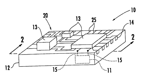
[0013] FIG. 1 is a perspective view of an electronic
module including an embedded capacitive structure therein
according to the invention.
[0014] FIG. 2 is a cross-sectional view of the
electronic module of FIG. 1 taken along line 2-2.
[0015] FIGS. 3 and 4 are cross-sectional views also
taken along line 2-2 of FIG. 1 and illustrating a method
for making the embedded capacitive structure according to
the invention.
CA 02413369 2002-11-29
[0016] FIG. 5 is a graph of material shrinkage versus
time for various dielectric materials used for making
embedded capacitive structures according to the
invention.
[0017] FIG. 6 is a graph of material shrinkage versus
temperature for the dielectric materials used for making
embedded capacitive structures according to the
invention.
[0018] FIG. 7 is a bar graph of measured capacitance
values for twelve different embedded capacitive
structures made according to the invention.
[0019] FIG. 8 is a graph plotting the measured
capacitance values of FIG. 7 versus surface area.
Detailed Description of the Preferred Embodiments
[0020] The present invention will now be described
more fully hereinafter with reference to the accompanying
drawings, in which preferred embodiments of the invention
are shown. This invention may, however, be embodied in
many different forms and should not be construed as
limited to the embodiments set forth herein. Rather,
these embodiments are provided so that this disclosure
will be thorough and complete, and will fully convey the
scope of the invention to those skilled in the art. Like
numbers refer to like elements throughout, and the
dimensions of layers and regions may be exaggerated in
the figures for greater clarity.
[0021] Referring now to FIGS. 1 and 2, an electronic
module 10 according to the invention including at least
one embedded capacitive structure 11 is first described.
The electronic module 10 includes a low temperature co-
fired ceramic (LTCC) substrate 12, for example, in which
6
CA 02413369 2002-11-29
the capacitive structure 11 is embedded. This material
offers advantages in terms of ruggedness, and an ability
to form recesses and small stable passageways therein, as
well as to provide electrical paths therethrough.
[0022] Furthermore, one or more electronic devices 13
may be mounted on a surface 20 of the LTCC substrate 12,
for example, as will be appreciated by those skilled in
the art. The electronic devices 13 may include
semiconductor devices, integrated circuits, heat coils,
resistors, etc., for example. Of course, other
electronic devices may also be mounted on the electronic
module 10. The substrate 12, as best seen in FIG. 1, may
carry electrical connectors 14 on at least one of its
surfaces. For example, the electrical connectors 14 may
be edge connectors for connection to a ribbon type cable,
as shown in FIG. l, for example. Of course, other
connectors may also be used, such as pins in a pin grid
array, as will be appreciated by those skilled in the
art.
[0023] The electronic devices 13 may be electrically
connected to the at least one embedded capacitive
structure 11 by conductive vias 15, for example. As seen
in FIG. 2, the embedded capacitive structure 11 may
include a pair of electrode layers 16 and an inner
dielectric layer 17 therebetween. The inner dielectric
layer 17 preferably has a high dielectric constant (K),
for example, greater than about 2000, and preferably
about 2400 or more, but values less than 2000 could also
be used. Because of its high dielectric constant, the
inner dielectric layer 17 allows high capacitance values
to be achieved with a relatively small surface area and
7
CA 02413369 2002-11-29
thickness. For example, the dielectric layer 17 may have
a thickness of less than about 3 mils, and preferably
about 1.5 mils, for example, yet provide a capacitive
density of 1000 pF/mm2 or more, as will be discussed
further below.
[0024] Additionally, more than one capacitive structure
11 may be embedded in the LTCC substrate 12. The
capacitive structures 11 may be arranged in a horizontal
plane, stacked vertically in an interdigitated fashion, as
shown in FIG. 2, or both, for example. As a result, the
electronic module 10 may include numerous capacitive
structures 11 with only a minimum amount the surface 20
area being required for connection thereto, as will be
appreciated by those of skill in the art. Thus, more area
of the surface 20 is available for integrated circuits,
etc.
[0025] Each capacitive structure 11 may further include
a respective first outer dielectric layer 18 adjacent each
of the electrode layers 16 and opposite a respective inner
dielectric layer 17. The dielectric constant of the inner
dielectric layer 17 is preferably greater than that of the
first outer dielectric layers 18. For example, the
dielectric constant of the first outer dielectric layers
18 may be less than about 100 and, more preferably, about
7-10, though other values are also possible. Such a
dielectric constant is closely matched to that of typical
LTCCs (i.e., ~8), which makes the dielectric layers 18
well suited for routing electrical signals through the
substrate 12, as will be appreciated by those of skill in
the art. Thus, one or more signal traces 30 may be
8
CA 02413369 2002-11-29
advantageously be formed adjacent the first outer
dielectric layers 18.
[0026] Also, the capacitive structure 11 may
optionally include a second outer dielectric layer 19
between each first outer dielectric layer 18 and a
respective electrode layer 16. The second outer
dielectric layers 19 preferably have a dielectric
constant greater than that of the first outer dielectric
layers 18 and less than that of the inner dielectric
layer 17. For example, the dielectric constant of the
second outer dielectric layers 19 may again be less than
about 100 and, more preferably, in a range of about 11-
14. The second outer dielectric layers 19 provide a
buffer between the inner dielectric layer 17 and
respective first outer dielectric layers 18, which
reduces the potential for interactions and provides
mechanical reinforcement and improved adhesion.
[0027] Turning now more particularly to FIGS. 3 and 4,
a method for making the electronic module 10 will now be
described. The LTCC substrate 12 is formed by arranging
the capacitive structures 11 between first and second
unsintered ceramic layers 21, 22. More particularly, the
first and second outer dielectric layers 18, 19 may be
positioned on the unsintered ceramic layer 21. For
example, the first and second unsintered ceramic layers
21, 22 may be tape layers, and the dielectric layers 17-
19 may also be tape layers. Of course, pastes or other
suitable delivery methods for the various materials may
also be used, as will be appreciated by those of skill in
the art.
9
CA 02413369 2002-11-29
(0028] A first one of the pair of electrode layers 16
is positioned on the dielectric layer 19, as seen in FIG.
3. The electrodes 16 may be screen printed, for example,
and may include at least one of Ag, Au, and Aged, though
other suitable materials may also be used. The inner
dielectric tape layer 17 is positioned on the electrode
layer 16, and the second one of the pair of electrode
layers 16 is positioned thereon, as shown in FIG. 4.
Another second outer dielectric tape layer 19 may then be
positioned on the stack, followed by another first outer
dielectric tape layer 18 (FIG. 2).
[0029] Of course, additional dielectric layers 17-19
and electrode layers 16 may be assembled to form the
interdigitated structure shown in FIG. 2. The second
unsintered ceramic layer 22 may then be positioned on the
capacitive structure (or structures) 11, and the stack
may be laminated and heated to sinter and form the
substrate 12. Additional dielectric layers may also be
used as necessary in particular applications, as will be
appreciated by those of skill in the art.
[0030] The conductive vias 15 may be formed using
standard techniques and are preferably made from the same
materials as the electrode layers 16, for example.
Signal traces 25 may also be formed on the surface 20 of
the electronic module 10 (e. g., by screen printing,
etc.), and one or more of the electronic devices 13 may
be mounted on the surface 20 and electrically connected
to the conductive vias 15 and signal traces.
CA 02413369 2002-11-29
[0031) Of course, it will be appreciated by those of
skill in the art that the conductive vias 15 may be
formed during the arrangement of the various layers of
the capacitive structure 11. Furthermore, the capacitive
structure need not be formed directly on the first
unsintered ceramic layer 21. Rather, the capacitive
structure (or structures) 11 may be formed separately and
then stacked between the first and second unsintered
ceramic layers 21, 22.
[0032] Additional details and features of the embedded
capacitive structure 11 will now be described with
reference to an example thereof fabricated according to
the invention.
EXAMPLE
[0033] Several multilayer capacitive structures 11 were
fabricated according to the invention using a system of
ultra-low firing temperature COG and X7R dielectric
compositions from Ferro Electronic Materials of Penn Yan,
New York (hereafter OFerro~). The embedded capacitive
structures were designed to include a high-K (2400) inner
dielectric layer 17 in a low-K (~10) dielectric package
(i.e., the second outer dielectric layers 18) made from
the above ultra-low firing dielectrics. These dielectrics
fire at temperatures below 950°C and are compatible with
standard gold metallization systems. The combination of
dielectrics provided a capacitive structure 11 that was
comparable to current LTCC systems and well suited for
integration into IC packaging or discrete, multi-function
passive component applications.
11
CA 02413369 2002-11-29
[0034] The test structures were 58 cm2 and were
fabricated and analyzed for material interaction and
electrical performance. Capacitance densities greater
than 1500 pF/mm2 were attained, as will be discussed
further below. The test structures were also made using
existing LTCC processing technology. More specifically,
standard tape casting, lamination and metallization
methods were used, thus providing for cost effective
manufacture of the capacitive structures 11 and
electronics module 10.
[0035] The Ultra-Low Fire series of X7R and COG
dielectrics by Ferro includes both low-K materials (K~10-
14), which were used for the first and second outer
dielectric layers 18, 19, and the high-K (K~2400, X7R)
capacitor dielectrics which were used for the inner
dielectric layer 17. Although these compositions densify
at temperatures below 950°C, they are not ceramic filled
or recrystallizing glass materials. Rather, they are
polycrystalline ceramics with less than 15 wt.o glass
forming constituents to promote densification by liquid
phase sintering. Further, they are compatible with low
resistivity, high Ag content and Au metal systems.
[0036] The physical property characteristics for the
three dielectric compositions used are given in Table 1,
below. The K10 and K14 dielectrics respectively used for
the first and second outer dielectric layers 18, 19 were
Ca0-Mg0-Zr02-SiOz based compositions. Further, Ca0-Mg0-
Zr02-Ba0-Si02 based compositions may also be used, for
example. The K2400 dielectric used for the inner
dielectric layer 17 was a doped barium titanate (BaTi03)
12
CA 02413369 2002-11-29
based X7R formulation. To achieve the ultra-low firing
behavior, the median particle sizes were kept small and
the distributions very narrow, making corresponding
surface areas higher than typical dielectric compositions.
Table d - Powder Physical Properties
Material Median Surface Density Tap LOI
Particle Area (g/cm3) Density (wt.o)
Size (mm) (mz/g) (g/cm3)
K10 0.7 12.4 3.2 0.60 1.6
K14 0.9 5.9 4.4 0.85 0.5
K2400 0.8 4.0 6.0 1.4 0.6
[0037] The above dielectric materials are produced on a
large scale as deagglomerated powders that can be directly
dispersed in a suitable organic binder system for tape
casting. Adjustments to compensate for the higher powder
surface area effect on tape casting slip rheology are
accomplished by the correct selection of dispersant
chemistry, order and method of addition and volume
concentration, as will be appreciated by those of skill in
the art. The tape system used for the test structures,
provided by Ferro, are described below in further detail.
[0038] A comparison of the densification behavior of
the three dielectric compositions, i.e., K10, K14, and
K2400, are illustratively shown in FIGS. 5 and 6. The
lines 31-33 respectively correspond to the K10, K14, and
K2400 materials in FIG. 5, and the lines 34-36
respectively correspond to the K10, K14, and K2400
materials in FIG. 6. The test structures were prepared as
tape cast laminates with a geometry of 12 x 12 x 1 mm,
though other geometrics may also be used. As may be seen,
the onset of densification occurs between 500 and 600°C,
13
CA 02413369 2002-11-29
while the most rapid densification takes place between 750
and 900°C. Mismatch between the densification rates and
total shrinkage of the dielectrics can also be seen in
these figures. Selection of proper cofiring profile
allowed for successful fabrication of composite
structures, as will be appreciated by those of skill in
the art.
[0039] Electrical property measurements were performed
on each dielectric material using both bulk ceramic and
standard 1206 size MLCC configurations. Dielectric
constant, dissipation factor and transmission coefficient
were characterized on bulk specimens using a Kent resonant
mode dielectrometer. One port and 2-port cavity
perturbation methods were used to measure Q*f and tf
values. Table 2 provides a summary of the low frequency
MLCC test results for parts fired at various temperatures.
Table 2 - Electrical Data Summary for Individual
Dielectric Materials in MLCC Form
Material Firing Cap K MHz DF MHz TCC
Temp (pF) ($) Q (ppm/C)
(o) _
(C) -55C 85C 125C
K10 900 28.4 9 0.001 84600 +134 +121 +119
920 29.1 9 0.001 1043?0 +134 +121 +119
940 29.4 9 0.003 3876 +132 +120 +121
K14 880 48.1 13 0.005 44315 0 +1 +6
900 49.7 14 0.001 39890 -9 -4 +1
920 50.0 14 0.001 37020 -16 -8 -3
K2400* 880 151.2 2338 1.49 N/A -10 -2 -2
900 157.7 2378 :1.49 N/A -10 -5 -6
*TCC Reported in o/°C
[0040) The data in Table 2 was generated at 1 MHz using
a HP 4278A capacitance meter and a HP 16034E test fixture.
The temperature coefficient measurements were performed
14
CA 02413369 2002-11-29
using an Ingalls Engineering model IE-TCM-80 temperature
chamber and capacitance test system using a lKHz test
frequency. High frequency test results for the low-K
materials are shown in Table 3. In their individual
forms, the K10 and K2400 dielectrics provide acceptable
COG and X7R performance, respectively, while the K10 data
illustrates this material's suitability as a low-K, low-
loss substrate dielectric.
Table 3 - High Frequency Electrical Data
Summary for Bulk Ceramic Samples
Material Firing Fired s' tan 5 Q*f if*
Temp Density (%) (GHz) (ppm/C)
(C) (~3/cm3)
K10 900 4.26 8.3 0.083 11215 -23.8
@
9.3 GHz
K14 900 3.25 13.4 0.14 6250 @ -10.6
8.8 GHz
* -20 to +80C
[0041] In the fabricated devices, the K10 materials
were used for the first outer dielectric layers 18 to
allow for conventional signal and power/ground planes, as
needed. The inner dielectric layer 17 made of the K2400
material was "sandwiched" between a second outer
dielectric layer 19 of K14 material. As noted above, the
K14 material provides a buffer layer between the K10 and
K2400 materials, reducing the potential for interactions
and providing mechanical reinforcement and improved
adhesion.
[0042] Baseline capacitor plate areas and geometries
were calculated using the following formula:
CA 02413369 2002-11-29
0.244 ~ K ~ S(n - 1)
C d
where K is the dielectric constant, S is the plate area, d
is the plate thickness, and n is the number of layers.
Embedded capacitive structures 11 with capacitances of
0.01, 0.015, 0.02 , 0.1, 0.15, and 0.2 uF were designed
and produced.
[0043] A modified tape transfer manufacturing process
was used to fabricate the test structures. Dielectric
tape was cast on a Mylar carrier film using a floating
doctor blade, and the tape thickness used was 25um for the
K10 & K14 materials and l4um for the K2400 material.
Internal conductors were deposited using a vision aligned
screen printer. A PVB binder system, Ferro B74001, along
with Ferro modifiers M1125 and M1135 were used with binder
solids loading adjusted for each dielectric composition to
help match green and fired shrinkage characteristics.
[0044] Moreover, Ferro "fritless" Au internal
conductors were used to construct the embedded capacitor
structure 11. The conductive vias 15 were formed by laser
drilling, and the holes were filled using conventional
LTCC methods. Lamination was performed in a heated
isostatic press. Final lamination time, pressure and
temperatures were comparable to conventional LTCC
processing. The test structures were fired on stabilized
zirconia setters and uniaxially constrained with a load
suitable to maintain flatness during sintering. Following
sintering, Au metallization was printed on the surface to
provide contact with the embedded components.
16
CA 02413369 2002-11-29
[0045] To understand the interactions taking place
between dielectrics and the conductors during co-firing,
a detailed microstructure analysis was conducted using a
JEOL scanning electron microscope (SEM) in both secondary
and backscatter detection modes with a PGT energy
dispersive X-ray analyzer (EDAX). The test structure
used a Ag/Pd (90:10) electrode system and demonstrated
the ability to sandwich a high-K dielectric between
layers of low-K material.
[0046] Capacitance was measured using a calibrated
hand held Tenma meter directly probing the conductive
vias 15 after the initial firing cycle. Post fire
surface metallization was added, and the structures were
processed through a standard 850°C, 10 minute dwell firing
cycle. Capacitance was again measured utilizing the same
equipment. Results of this testing are presented in
FIGS. 7 and 8. As may be seen, high capacitance
densities were achieved in these structures. The
embedded capacitive structures 11 had values close to the
design capacitance and showed no significant degradation
after a second firing cycle.
[0047] Many modifications and other embodiments of the
invention will come to the mind of one skilled in the art
having the benefit of the teachings presented in the
foregoing descriptions and the associated drawings.
Therefore, it is to be understood that the invention is
not to be limited to the specific embodiments disclosed,
and that other modifications and embodiments are intended
to be included within the scope of the appended claims.
17