Note: Descriptions are shown in the official language in which they were submitted.
CA 02413439 2002-12-03
14765ID 1
PM7~ i~leasu.~etttet~.t ~~ae~. Co~eaperts~ativra
W eld of th.~ invsntior~
this invention relates to apparatus and methods for
measuring and compensating PMD in optical systems using
the polarization bit interleaved (PBI) data structure.
B~,ckg~ound to th,e ira~rutio~
Fibre-optic transmission systems are now being developed
for tens of gigabits-per--second (Gbit/s) communication
channels, v~rhilst large volumes of 10 Gbit/s systems are
being fully deployed into existing networks. Various
potential limits are agproached as the performance of
such transmission systems is pushed further. Tt~.e
phenomenon of polarisation mode dispersion, PMD, is a
problem recently attracting a great deal of attention
from the telecommuni<:ations industry. PMD is a type of
distortion that varies froze fibre to fibre a==d is
typically o~= greater magnitude in oldf~r fibres. PMD is
also a random phenomenon, varying with both time and
optical frequency. ~~Thilst serJice providers are reluctant
to invest in new fibre routes, PMD may restrict the
deployment of new systems over the older fibre routes of
their network. In a small r~uznbey~ of fibres, PMD will give
rise to distortions so large that a lOGbit/s optical
transmission system cannot be reliably deployed over the
route. The impact of PMD scales linearly with system bit
rate, hence PMD will become a greater problem as the bit
rate of systems are increased. It is for these reasons
that PMD solutions have to be found.
PMD is a fundamental characteristic of both optical
fibres and optical components. It arises from the
consideration that single mode fibre can actually support
CA 02413439 2002-12-03
14765ID
two G,reakly guided modes that are orthogonall y polarised.
In other ;nTords, given an ideal fibre, a pulse can be
launched into either of these two polarisation modes and
propagate through the fibre in that polarisation mode
alone. ~ fiber exhibits slightly dii_ferent refractive
indices along different axes, a physical characteristic
known as birefringence. Birefringence=_ arises from a
variety of intrir~sic and extrinsic features of the fibre
manufacture. These features include geometric stress
caused by a noncirc~.lar core, and stz:ess birefringen~~e
caused by unsymmetrical stress of the core. Other
sources of birefringence include extern<~1 manipulation of
the fibre. External farces w~_11 include squeezing the
fibre, bending the fibre and tv=fisting of the fibre
In a birefringent fiJ~>re, the propagation speed will vary
with the launch polar°isatf.an state into the polarisation
modes of the fibre. Consequently, when proportions oz the
pulse are launched into bath polarisation axes they
travel at differerlt speeds and hence arrive at different
ti~r:es. The magnitude of the difference in arrival tim~as
between the fastest and slowest paths along the trao
Principle Mates of Polarization ;PSPS}} through the
fibre is known as the differential group delay (DGD}.
The receiver of a di rect deter tior~ apt~ical transmission
system does not distinguish bet~~=een the different
polarisation modes, but simply detects the combination of
the different polarisation modes. ~ize difference :in
arrival times of the pulse through the: two palarisati«n
modes will degrade the quality of the received data.
In a long length of fibre the birefringence is expected
to be weak but vary randomly along its entire length.
CA 02413439 2002-12-03
14765ID 2
This leads to random mode coupling a:Lang the fibre, a
process by which the pulse will continuously couple power
between the tcvo polarisation modes of the fibre. The
phenomenon of PMD re~_ates to the random variation of the
DGD of the fibre. TYie DGD is expected. to vary randomly
over time due to random variations of the fibre
birefringence as a result of enviranme:ntal effects, such
as temEperature. A c<.>nsequence oz this random variation
means that the instantaneous DGD of <~ fibre cannot be
predicted. instead the DGD of a fibre must be described
statistically. The fibre DGD also varies over
frequency/wavelength.
The DGD is the first-order consideration of P.~~D. Tt makes
the assumption that the PMD characteriwtics of a fibre
are constant over the band~~~idth of the transmitted data
signal. Higher-orders. of PMD are cansi<~ered ~~he~b the PMD
characteristics car r.o longer be considered constant aver
the bandxJvidth of a signal. Higher-order PMD relates to
the Uar.iation of the PMD characteristics of_ a fibre with.
frequency.
In order to compensate for first order PTv~D, it has been
proposed to use a delay line ~~~hich provrides differential
delay for different po?arisation states. in order to
re~rerse the system fiber DGD. A particular class of
fibres, known as high birefringence (~-~i-Di) fibres, has
been engineered deliberately to have T,rery high, uniform
birefringence for this purpose. The fibres hazre two
cleany definable axes wi th different refracti~re indices.
The propagation speed of a pulse wi~~- differ greatly
between each axis.
° CA 02413439 2002-12-03
14765ID 4
Three categories of techniques are used for PMD
compensations. They are all-optical, all electrical, and
hybrid.
For all-optical PMD compensation, the restoration of PMD
distortion is done optically without any optical-
electrical conversion.. The signal rema=ins in the optical
domain, Normally, all-optical PMD compensators consist of
a polarization controller and a fixed birefringent delay
element, such as a piece of high birefringence optical
fiber. The basic concept is to align the principal
states of po1_arization (PS~~ of the fiber with the
principal axes of the birefringent delay element to
reverse the DGD of the system fiber.
In the all-electrical method, the distorted optical
signal is converted to an electrical signal at the
receiver. A delay line filter with specific weights is
used to partially compensate for the distortion due to
PMD .
Hybrid PMD cornpensatior~ is a technique that uses both
optical anal electrical methods e the distortion
to restor
due to PMD. Far ex~~.mple a polarization controller (PC)
and a polarization beam sputter (PBS can be used to
transform the states of polarization, and split the
polarization components. At each output of the CBS, a
high-speed photo-detector converts the
optical sigr_al
to
electrical signal. An electrical line is used to
delay
adjust the phase delay between the two electrical
signals.
Problems with the known compensation techniques arise
from the need to determine principal states of
CA 02413439 2002-12-03
14765ID 5
polarization of the ~~ystem, and also the need to evaluate
the PMD to be corrected.
In polarization bit interleaved (PBI) optical
communications systems, adjacent pulse; in a transmitted
signal have orthogonal polarization. PMD then has the
most significant effect when these orthogonal
polarizations correspond to the PSPs of the transmissa.on
fiber. For bit interleaved signals, the all-optical PMD
compensator described above h~.s limited efficacy. PMD
compensation is also therefore snore difficult for PBI
systems.
There are also diff:icult~_es in measuring the PMD i.n a
system. Methods for measuring PMD can be 'aroac~ly
categorized in tTn,To g~~oups: methods that. make measuremer.,ts
in the time domain, ~~nd methods that m~~ke measurements in
the frequency ( or wave 1 en~fth ) dome in .
The modulation-phase--shift method ~.njects high-frequency
sinusoidal intensity mod~alatior~ l nta tlZe fiber, and then
measures the phase do=lay of the light exiting the fiber.
In performing this test the equipment changes the input
state of polarization (during the intensity modulation)
to find the maximum and minimum delay. At the maximum and
minimum delay the input state of polarization is aligned
with the fiber's principal axes. The phase difference
between the maximum and minimEum delay is then used to
determine the amount of PMD at that wavelength. To find
the PMD at another wavelength the souroe can be tuned to
another frequency and. the test repeated. This method thus
measures the instantaneous PI~TD at a particular
wavelength. This method is conceptually quite simple, but
it does require the experimental determination of the
CA 02413439 2002-12-03
14765ID 6
principal axes. In other words, the measurement must be
carried out many times with different input states of
polarization in order to determine ~,rhich states of
polarization correspond to the principal axes in the
fiber.
The modulation-pha~;e-shift method uses high-speed
intensity modulation and phase measurements to directly
measure the difference in propagation time for the t.wo
principal axes of the device under test.
The pulse-delay method is a direct measurement of the
difference in propagation time between pulses launched
into the t~rro principal axes. Implementing this method
involves launching very short pulses of light into the
fiber's two principal axes of polax-izatian and then
measuring directly the pulse delay between them. This
method, like the modulation phase sl:~ift method, also
requires experimentally finding the principal axes of
polarization.
she above techniques are all timerdaznain measurements.
~'recwency-domain measurements useq ei th~~r a source with a
broad spectrum (like an DED) or a tu.r~able laser. They
mare measurements over a U,ride range= of wavelengths .
Mathematically, measuring PMD over a wide range of
,wavelengths gives t:~e same average value of PMD as
measuring it at a csinala wavelength, but over a lo:~g
period of time. Thus, frequency-domain measurements tend
to provide the average PMD value.
Thus , i n the past, t:he measur ement of PMD in the systiam
has required cor.~plicated analytical processe;~,
particularly requiring test signals to be injected into
CA 02413439 2002-12-03
14765ID 7
the component. Furthermore, conventional PMD measurement
techniques require the orientation of the system PSPs to
be experimentally determined.
~ ~.~,r of ~h~ ~.n~e~~~.cax~.
According to a first aspect of t~.e invention, there
is provided a polarization mode dispersion (PI~ID)
campensatar for compensation of PMD i:n polarization ~>it
interleaved ~PBI~ optical signals comprising t;wo
interleaved bit streams, the compensator comprising:
a polarization controller;
a birefringent element;
a converter for converting an apt~ical o~.~jtput to an
electrical signal; and
an analyser fo:Y~ analysing at least one seleet.ed
spectral component of the electrical s~.gnal, 4vherein the
orientation of a signal entering the bi_refr-._nger~t element
is controlled by the palarizatior~ controller in
dependence an the electrical signal power of the at least
one spectra- component, having a freq~a.ency car..Lesponding
to the bit frequency of the two bit ;streams which form
the bit ir3terleaved signal.
The invention is based on the recognition that analysis
of tie electrical power spectrum at the output of a
compensator can be used to provide control of the
compensator for systems using PBZ: signals. In
particular, minimising a spectral component having a
frequency correspond~..ng to the bit freqwency of the two
bit streams which form the bit interleaved signal results
in alignment of the signal in the system at 45 degrees to
the two principal axes of the system (the syste:m
comprising the components in which PMD arises as well as
the compensation element). Thus, a control scheme which
CA 02413439 2002-12-03
14765ID 8
minimises this spectral component will provide the
desired polarization alignment for a PBI system.
The compensator may comprise a filter for extracting t:he
at least one selected spectral component of the
electrical signal.
The control scheme ma.y rely upon at least first a.nd
second spectral components, the first having a frequency
corresponding to the bit frequency of t.'r~e two bit streams
which form the bit interleaved signal arid the seccnd
having a frequency not equal to an integer multiple of
the bit frequency of the two bit streams. As discussed
above, the power of the first spectra:L component should
be minimized, but in addition, it can be shown that
maximizing the power at frequencies not equal to an
integer multiple of the bit frequency of the tlrao bit
streams results ~n mi:nimized overall PMI~.
To take these two factors into account, it is possible
to
maximize the rati o of powers of the second arid first
the
spectral components, to maximize the differerx~ce
or
between the second and irst spectral components. In
f
either case, the second spectral camp>onent
may have a
frequency of approximatelyhalf the bit frequency of the
two bit streams the bit interleaved
which form signal.
The invention also provides a method of providing PMD
compensation for compensation of PMD in PBI optical
signals comprising wo ir~ter3ea~red bit streams, the
method comprising:
passing the signal through a birefringent element,
and controlling the polarization at the input to the
birefringent element;
CA 02413439 2002-12-03
14765ID 9
con~rerting the optical output from the birefringent
element to an electrical signal;
measuring the electrical signal power at a first
frequency corresponding to the bit frequency of each of
the two bit strear~~s which form the bit interleaved
signal; and
using the measured electrical signal power as a
control parameter for. controlling the polarization at the
input to the birefrir.gent element.
This method pro~rides on
the compensation
control based
the electrical signal. wer spectrum, particularly at the
po
bit frequency of the two bit streams. Again, the
elec trical signal power at a second f_equency not equal
to of the bit frequency of the two
an integer
multiple
bit streams which farm the bit interleaved signal may
also be measured.
According to a second aspect of the invention, there is
provided an apparatus For estimating aMD in an optical
component through which a PBI optical signal has
propagated, the apparatus comprising
a converter for converting an optical output from
the component to an electrical signal; and
an analyser for analysing at least selected spectr<~l
components of the electrical signal, the PMD in the
optical component being derisred from the electrical
signal power at a frequency corresponding to the bit
frequency of the bi t interleaved signa=_ and from the do
signal power.
This aspect of the in~rentian is based on recognition that
analysis of the electrical power spect~°um at the output
of system can be used. to provide an estimate of the PMD
CA 02413439 2002-12-03
14765ID 10
in the system, for PBI systems. In particular, the PME
can be derived froir~ the do power and the bit frequency of
the PBI signal.
The bit frequency of the bit interleaved signal may be
40GHz, formed from two bit streams of 20Gbits/s.
The analyser may comprise a filtez: arrangement for
extracting the spectral components of the electrical
signal.
The second aspect of the invention also provides a method
for estimating PMD ivy an optical component through which
a PBI optical signal has propagated, the method
comprising:
converting the optical output to an electrical
signal;
measuring the electrical do signal power and the
electrical signal porNer at a frequency corresponding to
the bit frequency of the bit interleaved signal; and
deriving the level of PMD from the two electrical
signal powers.
The level of PMD may in particular be derived from the
ratio of the two electrical signal powers.
33rief e9.e~cri~t~.on o~ the d~~.v~r~.rags
Examples of the invention will now be described in detail
with reference to the accompanying drawings, in which:
Figure 1 is used to explain the nature of
polarization bit interleaved {PBI~ signals;
Figure 2 shows one example of a PivID compensator
according to the invention; and
CA 02413439 2002-12-03
14765ID 11
Figure 3 shows one example of an apparatus for
estimating PMD according to the invention.
Detailed descriptis~zr.
Figure 1 shows a polarization bit interleaved (PBI)
signal. Arrows 2,4 indicate orthogonal axes, and the
signal is made up from two bit streams 6r 8 having lir:.ear
polarization aligned with the axes 2,4. Axes 1~
represents time. Each bit stream has the same bit
Frequency, and the two streams are staggered with respect
to each other.
To generate the P:BI signal, a single return to zero pulse
train is generated and is provided oi~ two paths. each
path i s provided with a modulator so that the t~lro bit
streams are generated. one pulse train is delayed with
respect to the other, and the polarizations are
controlled before cambining the pulse trains to form the
PBI signal. The PBZ signal has double the bit rate of
the individ~.al bit streams. The separatian of the two
pulse streams using polarization reduces interference
between sequential pulses in the cambined PBI signal
resulting from dispersion.
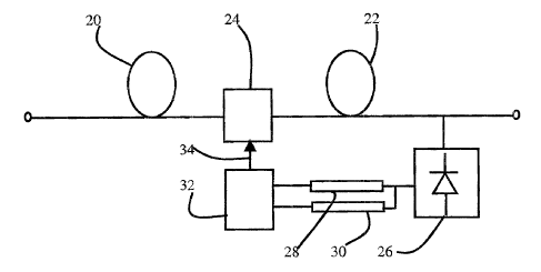
Figure 2 shows one example of a PMD compensator according
to the invention. The PMD campensator is for
compensating for PMD in any component, for example a
length of system fiber 20 as shown, ~;r,~hich may comprise
the span between nodes in a communications system. A
length of high birefringence fiber 22 is provided, and a
polarization controller 24 controls thE: launch angle into
the fiber 22. Varying the launch ancxle influences the
effect of the fiber 22, either to cancel the system PMD
or to compound the PMD. The polarization controller can
CA 02413439 2002-12-03
14765ID 12
be considered to alter the orientation of the overall
system PSPs, and thereby alter the orientation of the
PSPs with respect to a signal in the system.
Before describing the further components of the
invention, the theory underlying the invention will first
be described.
The invention is based on the recoc~n'_tion that spectral
analysis of the output of a system using PBI signals can
be used to provide information concerning the PMD in the
system, and can also be used to provide control of a
compensator, particularly to provide signal orientation
rrEidway between the P~?s of the system.
The invention follows from an analysis of the electrical
output power spectruzr from a system in which PBT signals
propagate. It can be shown that the electrical poorer
spectrum is given by:
s(~)-1-4(1-Y)Ysin'(wazl2) ... (1)
2T
+ 2~~ ( ~Y -1 1 2~L' c~~ 2rtL . . (
1 ~a _ ~2' _ 2 )
cos
2T T L=ODD T T
+ 2~~ 1 + cos 2~ Co
1 82' -
2~=
(
3
?
2T T L=~~~N T T .
.
.
In this equation:
T is the bit rate per cnannel (so for 2x20GF~~
channels interleaved t:o roan the PBI signal, T=50ps)
d~ is the PMD for. the system (which will include the
PMD compensator when provided
y is the proportion of power launched .into the
principal states (i.e. ~/=1 and y=0 correspond to launch in
CA 02413439 2002-12-03
14765ID 13
the two principal states, and 'y=0.5 corresponds to a 45°
launch state)
is the delta function, and
cs~ is the angular frequency.
S
Term (1) of this equation is a broadband power term.
This term has a maximum value when ~=~. or Else vrhen the
sine term is zero, namely when ~z.t~t is zero. Minimising
the PMD for a particular frequency will have the effect
of minimising the l~'c. U) term, and term { 1 ) will as a
result be maximised.
Thus, one control scheme for minimising the PMI7 is to
seek to maximise Term {1) for a chosen frequency. This
IS chosen frequency can be any frequency {other than
frequencies which are G multiple of the chanr~el
frequencies as will be seen below).
Term {1) in fact defines a notch profile {providing the
launch state is not into the PSPs), with the notch at the
frequency ~.lherE ~~e.c~=~ {so that ~2=1 ,~ {2f) ) . Far example,
for a frequency of lOGHz, a notch is present if the
system PMD is 50ps. When selecting a frequency to use as
the control parameter for P~zD compens~.tion, a frequency
would be selected which avoids this notch.
In practice, the total PMD in the system is likely to be
a maximum of around 25ps when compensating for a length
of transmission fiber {l5ps from the system fiber and
lops from the high birefringence compensatory. Thus, a
frequency of 20GHz or below should be selected as the
test frequency used for minimising the total PMD ~~'.
CA 02413439 2002-12-03
14765ID 14
Essentially, the control then involves tuning a launch
angle until Terrca (l) is maximised for the selected
frequency, which will taken as lOGHz by way of example.
Term ~2} defines a series of delta functions at odd
multiples of the basic PBI frequencies. Far example, if
the PBI signal is 2x20GHz bit streams, Term (2) defines
delta functions at 20GHz (L=1), 60G:~Iz (L=3) etc. In
practice, the bar..dwidth of the receiver is not
significantly greater than the combined bit rate (40GHz
in this case) so that the only term of interest is L=1,
namely 20GHz in this case.
This term is zero ~~fhen (2~--1}=0. In other words, this
term is zero when the y=~I2, namely when the launch state
is at 45 degrees to the two PSPs of the tatal system. As
mentioned above, this minimises the penalty for a gi.~,Ten
level of PMD in a PBI system. Thus, an optimal E'MD
compensation strategy will include minimisation of this
frequer~cy component .
Term (3} defines a series of delta functions at even
multiples of the basic PBI frequencies. Tr~is term is
independent of the launch state. Again, if the PBI
signal is 2x20GHz bit streams, Term (3) defines delta
functions at DC ( 0 Hz } (L=0 ) , 40GHz ~L---2 ) eto . The only
terms of interest are L=0 and L=2 namely 0 Hz and 40G~-3z
in this case. The delta function at OHz is dominant over
the braadband term (,2), so that measurement of the DC
power level effectively provides an e:~t~.mation of Term
(3) for L=0.
The ratio of Term (3) between the L=2 value (40GHz) and
the L=0 value (0Hz) has only a variable term in ~~ (all
CA 02413439 2002-12-03
14765ID 15
other values are knoGm constants). Thus, comparing the
4flGHz and DC components can provide an evaluation of the
level of PMD.
As described above, minimising Term (2) brings the launch
state to~rards 45 degrees, which is desired for PDI
systems. In Itself, this does not necessarily minimise
system PMD but merely the penalty for a given level of
PMD. In particular, minimizing Term (2) (the 2flGH2 tone)
either minimises the DGD or else resu~_ts in launch at 45
degrees to the PSPs. As discussed abo~re, maximising Term
( 1 ) ( the lflGHz or othe-r_ tone between fl and 2 flGHz ) eit.~.er
minimises the DGD or else results in launch on tree PSPs.
Consequently a control scheme is preferred which combines
the minimisation of Term (2) with the maximization of
Term ('!) for a selected frequency (for example lflGHz).
In this way, the 2flGHz component is used to ensure that
the system tries to fly at 45 degrees to the PSPs in
conjunction with the lflGHz component to mins_m.ise the
total DGD in the system.
One example is to use as control. parameter Term f1)
Term (2) and to apply control to maximise this parameter.
In the 2x2flGbit/s example, provided the total DGD does
not exceed 25ps, this provides a monotonic signal which
moves in the optimal directions. Thus, for a given level
of DGD it results in transmission at 45 degrees to the
PSPs, and for a given launch state it minimizes the DGD.
A second exa~t-r.~ple is to use as control parameter
Term(1)/~'erm(~), and again to apply control to maximise
this parameter.
CA 02413439 2002-12-03
14765ID 16
These are two examples of control parameter, and there
are of course an infinite number of ~>arameters which can
seek to minimise the 20GHz tone and maximise the lOGHz
tone.
The above analysis assists in an understanding of the
remaining components in Figure 2. The output of the
compensator fiber 22 is converted to an electrical sigwa.l
using an opto-eLectr_ic converter 2c, r~~hich will typically
comprise a photodiode device. This provides a broadband
electrical signal. In oraer to measure the power at the
frequencies of interest,. first and second filters are
provided 28,3J. The first filter 28 provides the
component of the electrical signal at the frequency of
the two bit streams (20GHz in the example given). The
second. filter ~0 provides a different frequency, not a
multa.ple of 2u~GHz in this example. i3y way of example,
the filter 30 may provide the lOGHz component in this
example.
Power measurement circuitry 32 obtains the electrical
powers of these components, and defines a feedback leap
for controlling the polarization controller 24. The
circuitry provides a control signal 34 to the
polarization controller 2~. As discussed above, the
control signal is selected such that the 20GHz tone is
minimized and the other tone is maximized. This is
achieved by usir_g a control signal 34 which maximises tl~.e
ratio or the difzerence between the tones, as discussed
above .
Figure 3 shows an apparatus far estizrsati.ng PMD in an
optical component 40 through which a bit interleaved
optical signal has propagated. The optical component 40
CA 02413439 2002-12-03
14765ID 17
may be any optical component, and may include many
sections. For example, the component 40 may include the
system fiber 20 and the compensator 22,24 of Figure 2, so
that the effect of the compensator control on the system
PMD can be determined.
The output of the component 4~ is converted to an
electrical signal using an opto-electric converter 26,
which v,,Till again typically comprise a photodiode device.
A first filter 42 provides the d~: component of the
electrical signal and a second filt.ec 44 provides the
component at the PEsI bit frequency (40GHz in the exaanple
given).
A processor 46 derives the PMII7 in the optical component
40 from the electrical signal powers at these
frequencies.
The components of Figures 2 aa~~d 3 may be f ntegrated _into
a single system, for both PMD compensation and
measurement.
In the example abo~;re, the PBI is desc~~ibed as a 4GGHz
signal made ~..zp from two 20GBit/s bit streams. The
invention is, however, applicable to a.ny frequency of PBI
signal.
Also, in the example above the PMD control is based on
analysis of two tones. Hoc~Tever, it is possible and
within the scope of the invention to control PMD based
solely on minimizing the 2QGHz tone.
The polarization controller may op~.zcally rotate the
state of polarization o.= an input signal. However, it
CA 02413439 2002-12-03
14765ID 18
may instead physically rotate the input signal with
respect to the birefringent element. For example, the
birefringent element itself may be rotatable in order to
control the launch angle into it. A rotatable
birefringent element is i~~tended to fall withyn the
definition of a polarization controller, as this will
control the relative orientation of the signal and the
birefringent element.
Other ~rariations ~JiZ_1 be apparent to those ski fled in the
art.