Note: Descriptions are shown in the official language in which they were submitted.
CA 02413597 2002-11-27
s
Non-Contact Communication Between Device and Cartridge Containing
Consumable Component
The present invention relates to technology for non-contact
communication between a device such as a printer and a cartridge
containing a consumable component.
After being opened, for example, after a period of about 6 months, the
quality of the ink in ink units (ink cartridges) for ink jet printers may
deteriorate as a result of the environment in which it is used. High printing
quality thus may not be achieved sometimes, and the print head of the
printer may be adversely affected. An example of a way to deal with this
problem is to provide the ink unit with memory such as EEPROM, and to
make sure that data for specifying the expiration period. of the ink is stored
in memory. A transmitterlreceiver provided in the pr°inter main unit
can
communicate with the memory through contact terminals to read the data
concerning the expiration period of the ink. In addition to data related to
the expiration period, data such as that relating to the amount of ink
remaining in each ink unit may also be stored.
An alternative to contact type memory such as EEPROM is a
structure in which a non-contact type of memory element is provided, and
radio transmission is managed by a read/write sensor provided in the printer
main unit.
However, because of the breadth of the communication range, such
radio transmission featuring the use of non-contact type memory elements
can result in the accidental reading of data in memory elements different
fiom the intended memory element, that is, mixed signals. In the case of
color ink jet printers, for example, a plurality of different ink units for a
plurality of color inks are arranged at a short pitch from each other in. a
carriage (ink unit support member), sometimes resulting in erroneous
1-
PF04I19 Series Final
CA 02413597 2002-11-27
communication with adjacent ink unit instead of the untended ink unit.
Attempts were thus made to pre-store ID information unique to each
non-contact memory element, and to have the ID information first read ~y
the printer main unit, so as to ensure proper communication as each element
was distinguished through the use of the ID information during subsequent
communication. However, since the procedure for reading the ID
information includes a process for preventing mixed signals, referred to as
an anti-collision process, running the ID information reading process for
every communication process on each unit can result in a much longer
communication process overall.
Accordingly, an object of the present invention is to provide a
technique permitting more rapid non-contact com~.nunication between a
device and a cartridge containing a consumable component.
In order to attain at least some of the above ar.~d other related objects,
there is provided a device in which a cartridge housing a consumable
component can be installed. The device comprises: a cartridge holder :in
which one or more cartridges containing a consumable component can be
mounted and a transmitter/receiver capable of non-contact communication
while near the cartridge. The cartridge has a memory circuit comprising an
antenna capable of non-contact communication while near the
transmitter/receiver, a memory for storing data relating to the consumable
component, and a controller for controlling communication with the
transmitter/receiver and for controlling access to the memory. The memory
circuit has an anti-collision mode in which the transmitter/receiver checks
the ID of the cartridge, and an active mode permitting memory access upon
reception of a memory access command from the tran.smitter/receiver. The
memory circuit is capable of shifting from a state which is not in anti-
collision mode to active mode without passing through the anti-collision
mode.
In this structure, the memory circuit can shift to memory access
-2-
PF04I19 Series Final
' CA 02413597 2005-05-30
mode without passing through the anti-collision mode for checking the ID,
thus permitting more rapid non-contact communication than the
conventional devices.
According to an aspect of the present invention, the device is a
printer in which a plurality of ink units each equipped with an element
capable of storing data are to be mounted. The printer comprises an ink
unit support member for supporting the plurality of ink units, and
communication means for reading or writing data upon non-contact
communication with the element. The printer is characterized by
comprising: a first procedure in which, for each ink unfit, the communication
means communicates with an element provided in the ink unit to read
identification (ID) information stored in the element, and a second procedure
in
which the communication means communicates with the element provided in the
ink
unit supported by the ink unit support member while distinguishing the
element based on the ID information that has been read. The second
_ _ _ _~~-i~~fthaut- tl~e ~irs~ proEed-ure-berg rt~n if ~he~D ..info-rrn:ation
stored in the element provided in the ink unit has already been properly read
when the communication means starts communicating; with the element, so
that the communication means communicates with the element.
Accidental communication with other elements can be prevented in
this printer because, for each, ink unit, the communication means reads the
ID information stored in the element in the ink unit in the first procedure,
and communicates with the element in the second procedure while the
element is distinguished based on the ID information, so that the ID
information stored in the element can be used to check if the communication
is being made with a specific proper element.
Also, the second procedure is run without the first procedure being
run if the ID information stored in the element provided in the cartridge has
already been properly read when the communication means starts
communicating with the element, so that the communication means
-3-
PF04I19 Series Final
CA 02413597 2002-11-27
communicates with the element, thus shortening the time needed for the
communication process when the ID iz2formation has already been properly
read other than when powered on or the like.
The present invention may be realized in a variety of embodiments,
such as devices in which cartridges containing a consumable component CaI1
be mounted cartridges containing a consumable component>' memory
elements of memory circuits for cartridges containing a consumable
component printing devices (printers), computer systems comprising a
device in which cartridges containing a consumable component can be
mounted methods for operating such various devices, systems, or memory
elements computer programs for implementing the functions of such various
devices, systems, or memory elements recording media on which such
computer programs are recorded and data signals embodied in a carrier
wave including the computer program.
Embodiments of the present invention will now be described by way
of further example only and with reference to the accompanying drawings in
which:-
Figure 1 schematically illustrates the outer appearance of an ink jet
printer.
Figure 2 is an oblique view of the structure of the surroundings of the
carriage in the ink jet printez~.
Figures 3(a) and ~(b) schematically illustrate the positional
relationship between the memory elements and the
transmitter/receiver/receiver in the printer main unit.
Figure 4(a) and 4(b) illustrate the structure of the memory element,
and the internal structure memory element and read sensor.
Figure 5(a) and 5(b) show the contents of tb.e memory elemewt and
the manufacturing data among the contents.
Figure 6 illustrates the internal structure of the ink jet printer.
Figure 7 is a block diagram of the internal structure of the control
-4-
PF04I19 Series Final
CA 02413597 2002-11-27
circuit in the ink jet printer.
Figure 8 is a flow chart of the steps involved in the ID information
reading process (first procedure) and the memory access process (second
procedure) such as the process for reading data other than the ID
information or the process for writing data on the remaining amount of ink.
Figures 9(a)-9(e) illustrate the carriage operating sequence when the
transmitter/receiverlreceiver reads the ID information of the memory
element.
Figures 10(a)-10(d) illustrate the carriage operating sequence when
the transmitterlreceiver/receiver reads data other than the ID information in
the memory element.
Figure 11 illustrates the transition in operating modes of the
memory element 311.
Figure I2 is a flow chart detailing the communication between the
ink unit and printer main unit in the anti-collision process.
Figure 13 is a flow chart detailing the communication between the
ink unit and printer main unit in the memory access process.
Figure I4 is a flow chart detailing the process of reading from the
memory element 311 (steps S23 and S33 in Figure 13).
Figure I5 is a flow chart detailing the process of writing to the
memory element 311 (steps S24 and S34 in Figure 13).
Figure 16 is a flow chart of another example of the flow of
communication between the memory element and printer main unit
illustrated in Figure 8.
Preferred embodiments of the invention are described below in the
following order.
A. Outline of ink jet printer
B. Structure of carriage and surroundings
C. Structure of memory element and transmitter/receiverlreceiver
D. Internal structure of ink jet printer
_5_
PF04I19 Series Final
CA 02413597 2002-11-27
' E. Internal structure of control circuit
F. Operation of ink jet printer
G. Details of anti-collision process
H. Details of memory access process
I. Variants in flow of communication between printer main unit and
memory element
J~ Other variants
A. Outline of ink jet printer
An outline of an ink jet printer as the primary applicable printing
device as an embodiment of the present invention is described below.
Figure 1 illustrates a schematic view of such an ink jet printer.
A color ink jet printer is illustrated here. The color printer 10,
which is an ink jet printer capable of producing color images, is an ink jet
type of printer in which a total of 6 colors, including light cyan (LC) and
light
magenta (LM) in addition to the four standard ink colors of cyan (C),
magenta (M), yellow (Y), and black (K) are ejected. onto a printing object
(printing medium) such as cut paper to form ink dots, thereby forming an
image. A structure featuring the use of ink sets other than 6, such as the
standard 4 color ink set, may also be employed.
As illustrated in Figure l, the color printer 10 comprises a paper-feed
structure in which the printing object such as cut paper fed from above and
in back is ejected from the front. An operating panel 11 and a paper ejector
12 are provided in the front of the printer main unit 10, and a paper feeder
13 is provided in back. The operating panel 11 includes various operation
buttons such as an ink unit replacement button 111, and a display lamp 112.
The paper ejector 12 is provided with a paper ejector tray 121 that covers the
paper ejector opening when not in use. The paper feeder 13 is provided with
a paper feed tray 131 that holds the cut paper (not shown). The printer 10
may also be provided with a paper feed structure which permits not only
single sheets of a printing objects such . as cut paper, but also continuous
-6-
PF04I19 Series Final
CA 02413597 2002-11-27
printing medium such as paper rolls, to be printed.
B. Structure of carriage and surroundings
The structure of the carriage 20 and its surroundings are described
as the ink unit support member (or cartridge holder) inside the color printer
I0. Figure 2 is an oblique view illustrating the structure of the
surroundings of the carriage 20. The carriage 20 is connected to a carriage
motor 23 by a pulley 22 by means of a drive belt 2I, and is driven so as to
tr avel horizontal to a platen 25 along a sliding shaft 24.
An ink unit (ink cartridge) INC1 containing black ink, and 5 ink
units INC2 through INC6 containing b colors of ink are mounted on the
carriage 20. The bottom of the carriage 20 facing the printing paper is
provided with a print head IHl having a nozzle row for ejecting black ink
and.print heads IH2 through IH6 having nozzle rows for ejecting 5 colors of
ink, respectively. The nozzle rows are fed ink from the ink units INC1
through INC6, respectively, to eject ink droplets onto the printing paper so
as to print text or images.
The non-printing area on the right side within the movable range of
the carriage 20 is provided with a capping device 26 for sealing the nozzle
openings of the heads IH1 through IH6 when not printing, and a pump unit
27 having a pump motor (not shown in figure). When the carriage 20 moves
from the printing area into the non-printing area on the right side, the
carriage 20 comes into contact with a lever (not shown in figure), and the
capping device 26 moves up to seal the heads IH1 through IH6.
In cases where some nozzle opening of heads IH1 through IH6
becomes plugged, or in cases where it is required to forcibly eject ink from
the heads IH1 through IH6 when one or more ink units are replaced, the
pump unit 27 is operated while heads IH1 through IH6 are sealed by the
caps 261 and 262, and the ink is suctioned out of the nozzle openings by t;he
negative force from the pump unit 2 ~ . In this way, dust or paper particles
adhering around the nozzle opening arrays can be cleaned off, and air
PF04I19 Series Final
.~b
CA 02413597 2002-11-27
bubbles inside the heads IH1 through IH6 can be ejected along with the ink
on the caps 261 and 262.
Memory elements 31.1 through 316 capable of storing data are
provided individually on the surface in front (direction in which paper is
ejected) of each lllk unit INC1 through INC6. Although IlOt shown in
Figure 2, a transmitter/receiver/receiver serving as the communication
means for reading or writing data is provided, so as to face opposite the
memory elements, at a suitable location in the non-printing area on the left
side within the movable r angc~ of the care iage 20.
Figures 3(a) and 3(b) are schematic diagrams illustrating in
simplified form the positional relationship of the carriage 20 and ink units
INC1 through INC6, memory elements 311 through 3.16 provided for the ink
units, and the transmitter/receiver/receiver 30 provided on the printer 10
main unit (part of printer 10 excluding the ink units INC1 through INC6)
1S serving as the printer main unit. Figure 3(a) is an oblique view seen from
the front in Figure 2, and Figure 3(b) is a plan view seen from directly
above.
The ink units INC1 through INC6 housed in the carriage 20 are
detachable, and can be replaced as needed by the user when the ink is used
up, when the expiration date has passed, or when changed to another color,
etc.
Figure 3(b) shows that the transmitter/receiver/receiver 30 (more
exactly, the antenna of the transmitter/receiver/receiver 30) in the present
embodiment is of a size corresponding to about 2 sections of the ink units
(and the memory elements thereabove) on the surface where the memory
elements are disposed. As an alternative to such a size, the
transmitter/receiver/receiver 30 may be about a size corresponding to 1
section on the surface where the memory element is disposed, or even abowt
a size corresponding to 3 or more sections.
The transmitter/r eceiver/receiver 30 carries out reading of the ID
information in sequence from left to right, that is, from the first memory
_$.
PF04I19 Series Final
CA 02413597 2002-11-27
element 311 to the 6th memos°y element 316, and memory access
operations
including a data reading open ation for data other than ID information, and a
data writing operation for data such as data on the amount of ink remaining.
Details on such ID information reading operation and memory access
operations are described below.
C: Structure of memory element and transmitter/receiverlreceiver
The structure of the memory element 311 and
transmitter/receiver/receiver 30 are described below with reference to
Figures 4(a) and 4(b). Figure 4(a) is plan view illustrating the structure of
the memory element 311. The memory element 311 is a proximity type of
non-contact memory element capable of transmitting data with the
transmitter/receiver/receiver 30 within a distance of about 10 mm. Overall
it is extremely small and thin, and can be attached to a tax°get object
by
making one side adhesive a~s a seal. The other memory elements have
exactly the same structure as the memory element 311 and therefore will not
be described.
The memory element 311 comprises an IC chip 3111, a resonance
capacitor 3112 formed by etching a metal film, and a flat coil 3113, which are
mounted on a plastic film and covered with a transparent cover sheet.
Although not shown in Figure 4(a), the transmitterlreceiver/receiver 30 is
composed of a communication circuit 302 (Figure 4(b)) and a coil antenna
301 which is similar the antenna of the memory element 311, with power
supplied from the power source unit of the printer main unit 10 (Figure 1).
Power is supplied only when the transmitter/receiver/receiver 30 and
the memory elements 311 through 316 are proximate to each other.
Accordingly, no communication operation is carried out during
ordinar°y
printing operations when no electrical power is supplied to the memory
elements 311 through 316.
Figure 4(b) is a block diagram illustrating the internal structure of
the memory element 311 and transmitter/receiver/receiver 30. The
_0.
PF04I19 Series Final
CA 02413597 2002-11-27
transmitter/receiver/receiver 30 is composed of an antenna coil 301, and a
communication circuit 302 connected to a peripheral input/output component
(PIO) 54 in the printer main unit control circuit described below. The IC
chip 3111 of the memory element 311 is composed of a rectifier 3114, RF
(radio frequency) signal analyzer 3115, controller 3116, and memory cell
311'7. The memory cell 317_7 is an electrically readable/writable memory
such as a NAND flash ROM. The controller 3116 can be in the form of a
logic circuit performing control functions, or can be in the form of a
microprocessor performing control functions by running a program. As
used herein, circuits comprising an antenna, memory, and controller for
controlling non-contact comrnunication-based memory access, as in the
example of the memory element 311, are referred to simply as a "memory
circuit."
The antenna 3113 of the memory element 311 and the antenna 301
of the tr ansrnitter/receiver/receiver 30 communicate with each other to read
ID information in the memory cell 3117 or to carry out memory access. The
high frequency radio signals produced in the communication circuit 302 of
the transmitter/receiver/receiver 30 are induced in the form of a high
frequency magnetic field through the antenna 301. The high frequency
magnetic field is absorbed through the antenna 3113 of the memory element
311 and is rectified by the rectifier 3114, resulting in DC power driving each
circuit in the IC chip 3111.
Data, that is, ID information unique to each memory element, such
as the serial number of the element, are stored in advance in the memory cell
3117 of the memory element 311. The ID information should undergo a
writing process during the processing and manufacturing of the memory
element. The ID information can be read by the
transmitter/receiver/receiver 30 of the printer main unit, thereby allowing
each memory element 311 through 316 to be distinguished.
The memory cell 311'7 of the memory element 311 may contain
- 10-
PF04I19 Series Final
a CA 02413597 2002-11-27
7
manufacturing data of the ink unit INC1 to which the memory element 311
is adhered, data relating to the expir ation period, or the like. The data can
be read by the printer main unit and compared to the current date so as to
notify the user that the expiration date of the ink unit INCl is approaching.
Data on the remaining amount of ink in the in:l~ unit INC1 and the
like can be written to the memory cell 3117 in the present embodiment.
The data on the remaining amount can be read by the printer main unit, and
a report can be issued to the user when the amount is running out. The
memory elements 311 through 316 may also contain suitable data other than
the above.
Figure ~(a) is a table of the details of the data stored in the memory
cell of the memory element. As indicated in Figure ~(a), the memory cell
3117 comprises a veritable area 61 where data can be read and written by the
printer main unit, and a non-veritable area 62 where data can be read, but
not written, by the printer main unit.
The data written in the non-writable area 62 is written before the
memory element 311 is attached to the ink unit INC1, such as the process in
which the memory element 311 is fabricated or the process in which the in:l~
unit INC1 is manufactured. The printer main unit thus can read and write
data stoxed in the veritable area 61, but can only read, and not write, data
in
the non-writable area 62.
The veritable area 61. is divided into a user memory area and a
classification code memory area. Of these, the user memory area is used to
write data such as the remaining ink amount in the ink unit INC1. The
data on the remaining ink amount can be read by the printer main unit to
issue a report to the user when the ink is running out. A variety of codes for
distinguishing the ink unit type or the like can be also stored in the
classification code memory area, and the user can freely use these codes.
The non-writable area 62 serves as the area for storing the ID
information. Unique ID information for distinguishing the memory
.11.
PF04I19 Series Final
_.
CA 02413597 2002-11-27
~ element 311, including manufacturing data related to the ink unit to which
the memory element 311 is attached, are stored in the area for storing the ID
information.
Figure 5(b) is a table showing in greater detail the contents of the
area for storing the TD information. The area for storing the TD information
comprises an ink unit manufacturing data area 63 for storing various types
of manufacturing data related to the ink unit to which. the memory element
311 is attached.
Data on the year, month, date, time, minute., second, and location
where the ink unit was pxoduced can be stored in the ink unit manufacturing
data area 63. Each piece of data can be written to an area of about 4 to 8
bits, which will require a memory area of about 40 to '70 bits in total. The
manufacturing data 63 relating to the ink unit can be stored in the non-
writable area 62 and not in the user memory of the veritable area 61, so as to
allow that much more data to be written to the veritable area 61 of the
memory cell 3117.
When the ID information including manufacturing data on the ixik
units INC1 through INC6 is read from the memory elements 3I1 through
316 at a timing when the printer 10 is powered on ox the like, the user may
be notified that the ink unit expiration date is approaching, for example.
The memory cell 3117 of the memory elements 311 through 316 may
also include suitable data other than the above. The memory cell 3117 in
its entirety may constitute the veritable area, in which case, the entire
memory cell 3117 may be composed of an electrically readablelwritable
memory such as NAND type flash R,OM for storing memory element-specific
ID information such as the above ink unit manufacturing data.
D. Internal structure of ink jet printer
The internal structure of the color ink jet printer 10 is described.
below with reference to Figure 6. Figure 6 illustrates the internal structure
of the px.~inter 10 in the present embodiment.
-12-
PF04I19 Series Final
CA 02413597 2002-11-27
As illustrated, the printer 10 comprises a mechaniszn for driving the
print heads IH1 through IH6 on the carriage 20 to eject; ink and form dots, a
mechanism for moving the carriage 20 back and forth in the axial direction of
the platen 25 by means of a carriage motor 23, a mechanism by which a
printing object such as cut paper 133 fed from the paper feed tray 131 is
conveyed by means of a motor 40, and a control circuit 50.
The mechanism for moving the carriage 20 back and foxth in the
axial direction of the platen 25 is composed of a sliding shaft 24 that is
suspended parallel to the axis of the platen 25 to slidably holding the
carriage 20, and a pulley 29 with an endless drive belt 21 stretched between
it and the carriage motor 23.
The mechanism for conveying the printing object comprises the
platen 25, a paper feed motor 40 for rotating the paper feed auxiliary roller
(not shown in figure) and platen 25, gear mechanism 41 for transmitting the
rotation of the paper feed motor 40 to the platen 25 or the Like, and an
encoder 42 for detecting the angle of rotation of the platen 25. The
transmitter/receiverlreceiver 30 is located at a suitable position on the
inside
surface of the printer 10 casing (not shown in figure), such as specific
locations in the non-printing area on the left side of the carriage 20.
The control circuit 50 controls the operation of the paper feed motor
40, carriage motor 23, and print heads IH1 through IH6 while getting
signals from the printer control panel 13, transmitter/receiverlreceiver 30,
externally connected personal computer, or the like. Cut paper fed from the
paper feed tray 131 is set up between the platen 26 and paper feed auxiliary
roller, and feed in the prescribed volume at a time according to the angle of
rotation of the platen 25.
An ink unit INC1 through INC6 are installed on the carriage 20.
Ink cartridges INC1 through 6 are equipped with memory elements 311
through 316 for storing the amount of ink remaining, or the like. Ink
cartridge INC1 contains black (K) ink, and ink cartridges INC2 through 6
-13-
PF04I19 Series Final
CA 02413597 2002-11-27
r
are filled with cyan (C), magenta (M), yellow (Y), light cyan (LC), and light
magenta (LM), respectively.
E. Internal structure of control circuit
The internal structure of the ink jet printer control circuit 50 is
illustrated below with reference to Figure 7. Figure 7 is a block diagram of
the internal structure of the ink jet printer control circuit 50 in the
present
embodiment.
As illustrated in the figure, a CPU 5I, PROM 52, RAM 53, peripheral
inputloutput (PIO), timer 55, drive buffer 56, and the like are provided
inside
the control circuit 50.
The operating panel 11, personal computer PC, carriage motor 23,
paper feed motor 40, encoder 42, and transmitterlreceiver/receiver 30 are
connected to the PIO 54. The drive buffer 56 is used as a buffer to supply
on/off signals for forming dots to the print heads IH1 through IH6. These
are connected to each other by a bus 57, allowing them to get data from each
other. The control circuit 5 0 is also provided with an oscillator 58 that
outputs a drive waveform at a certain frequency, and a distributor 59 that
distributes the output from the oscillator 58 at a certain timing to the print
heads. IH1 through IH6.
When the power is on or the Like, the control circuit 50 allows the
carriage 20 to move to the non-printing area on the Left side of the
tr ansmitter/receiverlreceiver 30, and reads sequentially from the memory
element 311 disposed on the ink unit INC1 at the left end up to the memory
element 316 on the right end. The control circuit 50 thus obtained ID
information from the memory elements 311 through 316. Once the ID
information has been obtained from all the memory elements 311 through
316, memory access is processed as the memory elements 311 through 316
(and ink units INC1 through INC6) are distinguished on the basis of the ID
information. Details on the ID information reading process (first procedure)
and the memory access process carried out as the elements are distinguished
-14-
PF04I19 Series Final
CA 02413597 2002-11-27
:P
on the basis of the ID infomnation (second procedure) are given below.
F. Operation of ink jet printer
Figure 8 is a flow chart of the steps involved in the communication
process between the memory elements 311 through 3I6 in the ink units
INC1 through INC6 and the transmitter/receiver/receiver 30 in the printer
main unit, that is, the ID information reading process (first procedure)
and the memory access process (second procedure) ir.~cluding the process of
reading data other than the ID information and the process of writing data
related to the ink units such as data on the amount of xnk remaining.
10 The printer 10 runs a communication process routine with memory
elements 311 through 316 which is different from the communication process
that is run during the ordinary printing process, so as to read the
manufacturing data of the ink units or run a process such as the readlwrite
process of the remaining ink whenever (1) the power is turned on, (2) the
user replaces any of the ink units INCI through INC6 while the power is on,
(3) a predetermined time has elapsed since the prior communications process
has been run, and so forth.
At such times, the carriage 20 housing the ink units INC1 through
TNC6 f~xrst moves from the ordinary printing position or the x~on-printing
area on the right side to the printing area on the left side. The carriage 20
moves to the non-printing area on the left side to permit communication by
the memory element 311 or the like near the transmitter/receiverlreceiver 30
upon the reception of power from the antenna coil 301 of the
transmitter/receiver/receiver 30.
In the communication routine thus started in this manner between
the transmitterlreceiver/receiver 30 and the memory elements 311 through
316, the control circuit ~0 in the printer main unit IO determines whether or
not there has been a request to turn on the power (step s100). Specifically,
it is determined whether or not the operation of the ink jet printer 10 has
started. The request for power on is a signal that is produced to request
-15-
PF04I19 Series Final
CA 02413597 2002-11-27
r
communication with the ink units when the user presses the power button
on the printer 10 to supply power, also referred to as the "power on
notification." When it is determined that a power on request has been issued
(step s100= Yes), the first procedure, that is, the procedure for reading the
ID
information from the memory elements 311 through 316, is initiated (step
s104).
When it is determined that no power on request has been issued (step
s100~ No), the control circuit 50 determines that the printer 10 is in the
midst of the ordinary printing process, and it is then determined whether or
not an ink unit replacement request has been issued (step s102). The inl~
unit replacement request is a signal, for example, that is produced to request
communication with the ink units after the user has pressed the ink unit
replacement button 111 on the operating panel while the power is on to
replace any of the ink units II~TC1 through INC6, alsa referred to as the "ink
unit replacement notification."
When it is determined that an ink unit replacement request has been
issued (step x102: Yes), the control circuit 50 initiates the first procedure,
that is, the procedure for reading the ID information from the memory
element in the replaced ink unit (step s104). When it is determined that no
ink unit replacement request has been issued (step s102: No), it is
determined that the ID information of the memory elements 311 through
316 have already been properly read such as when the power is already on,
and the second procedure, that is, the memory access process with ~ th.e
memory elements 311 through 316, can be immediately started (step s200).
When the second procedure is started, the control circuit 50 first
issues an active mode command to the memory elements 31I through 316
(step s202). The active mode command is a command issued to the memory
elements 3II through 316 according to the ID information of each. When
the received ID information is crosschecked and found to be consistent with
the ID information of the memory elements 311 through 3I6, a memory
~16-
PF04II9 Series Final
CA 02413597 2002-11-27
access OK signal is transmitted to the transmitter/receiver/receiver 30.
When the control circuit 50 obtains an OK response to the active
mode command from all the memory elements 311 through 31C, the memory
access process for the memory elements 311 through 316 is executed (step
s204). In this way, when the TD information has already been propexly read
other than when the power is turned on or the like, the second procedure
starts without the first procedure being run, allowing the time needed for the
communication process to be shortened. The ID information reading
process (first procedures) should be run again when no access OK response is
obtained from any of the memory elements.
The control circuit 50 concludes this communication process routine
when the memory access process is concluded, and the data on the amount of
ink remaining is finished being written to the memory elements 311 through
316.
1 S When the control circuit 50 starts the first procedure, that is, the
procedure for reading the ID information from the memory elements 311
through 316 (step s104), the anti-collision process is then run (step s106).
The anti-collision process is a process for preventing mixed signals during
the process of reading the ID information from the memory elements 31.1
through 31.6 when no ID information has been obtained from the elements.
When the anti-collision process breaks down while being run, the anti-
collision process should be run after being restarted. The details of the
anti-collision process are given below.
Upon the conclusion of the anti-collision process, the control circuit
50 runs the process for reading the ID information from memory elements
311 through 316 (step x108). When the process for reading the ID
information is complete, the present communication process routine will be
complete, and the memory access process with the memory elements 311
through 316 will start (step s206).
When the control circuit starts the memory access process, the
-17-
PF04I19 Series Final
CA 02413597 2002-11-27
f
subsequent processes (steps s208 and s2I0) are the same as the
aforementioned steps s202 and s204, and will therefore not be described
again here. The present communication process routine is complete when
the memory access process is completed and the data on the amount of ink
remaining is finished being written to the memory elements 3II through
316.
The first procedure (communication process) and second procedure
(memory access process) involving the memory elements 31I through 316 in
ink units INC1 through INC6 and the transmitter~receiver/receiver were
described above, but as described below, the communication process with the
memory elements 312 through 316 is executed sequentially one at a time
from the memory element 311 on the left end to the xnemoxy element 316 on
the right end. At such times, the carriage 20 moves sequentially and stops
one ink unit at a time to r un the communication process for the memory
element of each ink unit. Alternatively, the movement and positioning of
the carriage 20 is preferably reduced using one of a size corresponding to
about 2 ink unit sections, such as the transmitter/receiver/receiver 30 in the
present embodiment, so it can move and stop a total of 3 times every two ink
units to run the communication process on two memory elements at a time at
each location.
The operation of accessing the memory elements 311 through 316 of
the ink jet printer 10 is illustrated below with reference to Figures 9 and
10.
Figures 9(a)-9(e) illustrate the operating sequence of the carriage 20
(and ink units INC 1 through INC6) when the transmitter/receiver/receiver
30 reads the ID information in the memory elements 311 through 316 while
the power is turned on or during the replacement of an ink unit.
Commands to run the ID information reading operations other than in these
cases can be carried out when the user runs printer driver software on the
screen of a personal computer or by using the operating panel 11 (Figure 1)
of the printer 10.
-18-
PF04I19 Series Final
CA 02413597 2002-11-27
The transmitter/receiver/receiver 30 (more exactly, the antenna) in
the present embodiment is of a size corresponding to about 2 sections of the
ink units (and the memory elements thereabove) on the surface where the
memory elements are disposed. When the transmitter/receiverlreceiver 30
stops the carriage 20 exactly between a given memory element and an
adjacent memory element, data can be transmitted to the two memory
elements. The transmitterheceiverlreceiver 30 reads or writes the ID
information sequentially from the left end in the figure, that is, from the
first
memory element 311, to the 6th memory element on the right end.
First, in an unaccessed state (step s110 of Figure 9(a)) where the
transmitter/receiverlreceiver 30 has not accessed any of the memory
elements 311 through 316, the carriage 20 is positioned to the right at some
distance from the non-printing area on the left side where
transmitterlreceiver/receiver 30 is located, preventing any of the memory
elements 311 through 316 of ink units INC1 through 6 from being accessed.
Next, while the ink unit INC1 is accessed (step slll in Figure 9(b)),
the carriage 20 moves up to the non-printing area on the left side and stops
at a location permitting data communication between the
transmitter/receiver/receiver 30 and only the ink unit INC1 on the left end.
That is, the right end of the antenna coil 301 of the
transmitter/receiverlreceiver 30 is in a position corresponding to about the
middle of the memory element 311, and in that position the
transmitterlreceiver/receiver 30 is too far from the memory element 312 of
the ink unit INC2 to be able to transmit data. In this embodiment, non-
contact communication betvveen the transmitter/receiver/receiver 30 and the
memory element is possible at a distance within about 10 mm, so the gap
between the transmitter/receiverlreceiver 30 and the second memory
element 312 at the stop position in Figure 9(b) is sufficiently greater than
10 mm. At this stop position, the transmitter/receiver/receiver 30 first
reads the ID information in the memory element 311. In other words., the
. lg _
PF04I19 Series Final
CA 02413597 2002-11-27
transmitter/receiverJreceiver 30 reads the ID information at apposition
where it is possible to distinguish the position of the first ink unit
targeted
for the ID check process. The operating mode of the memory element
during the process for reading the ID information is referred to as ''anti
s collision mode."
Because the ID information here includes manufacturing data
related to the ink unit INCI, when it is determined, for example, by the
printer 10 main unit that the expiration period of the ink unit TNC1 is
running out based on the date of manufacture, a report to the user can be
displayed on the screen of the personal computer PC or a display provided on
the printer 10 main unit.
The carriage 20 then stops at a location corresponding to I ink unit to
the right, and reads the ID information of the memory element 312 of the
second ink unit INC2 (s112 in Figure 9(c)). At this stop position, the
transmitterlreceiver 30 can still access the memory element 311, so in order
to prevent mixed data signals, the ID information of the memory element
311 which has already been read axe included in the ID information read
command (referred to as "anti-collision command") transmitted from the
transmitter/receiver 30 to the memory element 312. The ID information of
the memory element 311 is used to distinguish the memory elements 311
and 312, allowing the ID information to be accurately read from the memory
element 312. Alternatively, the memory element 311 may be automatically
removed from anti-collision mode when the process of reading its TD
information is complete, so that the memory element 311 does not receive
subsequent anti-collision commands.
The ID information of memory elements 313 thxough 316 of ink units
INC3 through INC6 is subsequently read in sequence in the same manner
(sll3 through sll6 in Figures 9(d) to (e)). After the ID information of the
final memory eleraent 31F has been read (sllC), the carriage 20 is returned
to the position in the nan-printing area on the right side, and the ID
-20-
PF04I19 Series Final
CA 02413597 2002-11-27
information read routine is complete. Because all the ID lllforzllatzon Of
memory elements 311 through 316 has thus been obtained, the printer 10
main unit can ascertain the arrangement of the ink units INC1 through
INC6. That is, the memory of the printer main unit stores the sequence in
which all of the ink units INC1 through INC6 are arranged in the carriage
20, where the ink unit INC1 corresponding to the ID information obtained
from the memory element 311 is disposed on the leftmost side, and the i.nk
unit INC2 corresponding to the ID information obtained from the memory
element 312 disposed in the adjacent position to the right. In other words,
IO in the aforementioned procedures, the ID informai~ion of each ink unit. is
checked while the position of an ink unit targeted for the ID check can be
distinguished, so that each ink unit and its ID information is stored in
memory in the printer main unit.
The following is a description of the operation by which the
transmitter/receiver 30 reads data other than ID information stored in the
memory elements 311 through 316 by using data concerning the relation
between the arrangement sequence of the ink units INCI through INC6 and
the ID information ascertained in the above steps. Figures 10(a)-10(d)
illustrate the operating sequence of the carriage 20 (and ink units INCl
through INC6) when the transmitter/receiver 30 reads data other than ID
information stored in the memory elements 311 through 316.
First, in an unaccessed state (step s220 of Figure 10(a)) where the
transmitterlreceiver 30 has not accessed any of the memory elements 311
through 316, the carriage 20 is positioned to the right at some distance from
the non-printing area on the left side where the transmitter/receiver 30 is
located, preventing any of the memory elements 311 through 316 of ink units
INCI through INC6 from being accessed.
Next, while the ink units INC1 and INC2 are accessed (step x221 in
Figure 10(b)), the carriage 20 moves up to the non-printing area on the left
side and stops at a location where the transmitter/receiver 30 can transmit
-21-
PF04I19 Series Final
'~ CA 02413597 2002-11-27
j
° data to the ink unit INC1 on the left end and the adjacent ink unit
INC2.
That is, the middle of the antenna coil 301 of the transmitter/receiver 30 is
in
a position corresponding to the area between the memox-y element 311 and
the memory element 312, and in that position the transmitter/receiver 30 is
capable of transmitting data to both memory elements 311 and 312 of ink
units INC1 and INC2.
The transmitter/receiver 30 transmits data read commands to the
memory elements 311 and 312 at the stop position. At that time, the ID
information of the memory element 311 which has already been read. is
allowed to accompany the first memory element 311. The memory element
311 receiving this command checks that the accompanying ID information is
actually the ID information of the memory element 311 itself, and transmits
the requested data other than the ID information back to the
transmitter/receiver. The same reading process is similarly carried out for
the second memory element 312.
The carriage 20 then stops at a location corresponding to 2 ink uxxits
to the right, and reads the ID information of the memory elements 31.3 and
314 of the second ink units INC3 and INC4 (s222 in Figure 10(c)). At this
stop position, data other than the ID information are read while the memory
elements 313 and 314 are accurately distinguished in the same manner as
the reading process for memory elements 311 and 312 above.
The carriage 20 is similarly moved and stopped 2 ink unit sections to
the right (s223 in Figure 10(d)), and the non-ID information of memory
elements 315 and 316 is read. The routine is then complete.
The carriage 20 is moved and positioned a total of 3 times by reading
the non-ID information while stopping the carriage 20 at positions where the
transmitter/receiver 30 can access 2 memory elements at a time, as in the
present embodiment. Although memory elements can be read one at a time
while moving and positioning memory elements one at a time, this
embodiment is more desirable because it can be completed with half the
-22-
PF04I19 Series Final
CA 02413597 2002-11-27
moving and positioning operations, thus shortening the time needed foi the
reading process as a whole. In general, when the transmitter/receiver 30
can communicate with N lllk units at the same position, the
transmitter/receiver 30 should be moved N ink unit sections at a time.
Ink unit-related data. such as data on the amount of ink remaining; in
ink units INC1 through INC6 can be written at any time through the
transmitter/receiver 30 to the writable area in the memory cell 3117 of the
memory elements 311 through 316. The writing operation in such cases can
be managed while the memory elements are accurately distinguished using
the ID information of the memory elements 311 through 316 which has
already been read, in the same manner as the process for reading the non-ID
information above.
G. Details of anti-collision process
Figure 11 illustrates the transition in operating modes of the
memory element 311. The memory element 311 has 4 modes: a power off
mode Ml, hold mode M2, anti-collision mode M3, and active mode M4,
Power off mode M1 is a sate in which no high frequency signals are received
from the transmitterlreceiver 30, and no power output is produced in the
memoxy element 311. When the transmitterlreceiver 30 and the memory
element 311 move to within about 30 mm of each other to allow the memory
element 311 to receive high frequency signals, the memory element 311
shifts from power off mode M1 to hold mode M2. Hold mode M2 may be also
referred to as a standby mode. The distance at which communication
becomes possible is preferably about 15 mm, and even more preferably about
10 mm.
When the memory element 311 receives an anti-collision start
command from the transmitterlreceiver in hold mode M2, it moves to anti-
collision mode M3. Anti-collision mode M3 is a mode for the anti-collision
process described above (ID information check). In the example illustrated
in Figure 11, when the anti-collision process is complete (that is, when the
-23-
PF04I19 Series Final
y CA 02413597 2002-11-27
ID information has been successfully checked), the memory element 311
automatically shifts to active mode M4. When the ID check breaks down
during the anti-collision process, the memory element 311 returns from
anti-collision mode M3 to hold mode M2. The details of the anti-collision
process will be described later. When the memozy element 311 is in anti-
collision
mode M3, the transmitter/receiver 30 can only check ID information of the
memory
element 311 through the anti-collision process but cannot perform other memory
access
operations on the memory element 311. The anti-collision. process can be
performed
only when the memory element 311 is in anti-collision mode M3.
Active mode M4 is a mode for accessing memory. When the memory
element 31I is in active anode M4, the transmitter/receiver 30 can read from
and write to the memory cell 3117 (Figure 4). When the memory element 31:l is
in a mode other than active mode M4, the transmitter/re;ceiver 30 cannot
perforn
memoay access operations on the memory element 311. The memory element 311
shifts to active mode M4 upon receiving an active mode command in hold
mode M2. As noted above, when the ID information has been successfully
checked, the element automatically shifts from anti-collision mode M3 to
active mode M4. The memory element 311 returns to hold mode upon
receiving a hold command in active mold M4.
The anti-collision start command includes a specific portion of the ID
information shared by a plurality of cartridges, allowing a plurality of
cartridges to simultaneously move to anti-collision. mode M3. The an.ti-
collision start command does not need to include IL) information, however.
The active mode command includes all cartridge ID information, allowing
only one cartridge memory element 311 to shift to active mode M4. The
hold command also includes all cartridge ID information. Including part or
all of the ID information in the commands which the memory element 311
can receive, as in this example, is more desirable in that it permits more
reliable access to the memory element 31I.
In this way, when the memory element 311 in the present
- 24 -
PF04I19 Series Final
CA 02413597 2002-11-27
embodiment receives an active mode command while in hold mode M2, it can
move directly from hold mode M2 to active mode M4 without undergoing an
anti-collision process. A resulting advantage is that the
transmitter/receiver 30 can issue an active mode coznznand for an ink unit in
which the ID information has been previously checked, so as to immediately
start the memory access process. Such an advantage is not limited to the
printer 10 as in the present embodiment, and will be obvious in devices in
which cartridges are generally not replaced very frequently. That is, in this
sort of device, once the ID of the cartridges has been checked by the an.ti-
collision process, the cartridge ID is already known, and the anti-collision
process therefore does not have to be carx°ied out again. The active
mode
command can thus be used to avoid having to carry out the anti-collision
process every time memos°y is accessed, resulting in the significant
advantage of more rapid memory access.
Figure 12 is a flow chart illustrating in detail the particulars of
communication between an ink unit (specifically, the memory element 37_1)
and the printer main unit (specifically, the transmi.tterJreceiver 30) in the
anti-collision process. This :Flow chart corresponds to the details of the
fiz°st
procedure illustrated in Figuk°e 8 (steps s104 through s108). The
example in
Figure 12 assumes that the transmitter/receiver 30 can communicate with
two ink units INC1 and INC2. The left side of Figure 12 shows the process
procedure on the printer main unit side, and the middle and right sides show
the process procedure for the first and second ink units, respectively.
When the anti-collision process is started, the transmitter/receiver
30 issues an anti-collision start command (step S11). When the two ink
units INC1 and INC2 receive an anti-collision start command, the process f:or
checking the ID proceeds between the transmitter/receiver 30 and the two
ink units INCl and INC2. Specifically, for example, t:he
transmitter/receiver 30 searches the ID bit value in the two ink units INC1
and INC2, beginning from the lower bits of the ID. 'rhe ink units INC1 and
-25-
PF04I19 Series Final
CA 02413597 2002-11-27
INC2 send a response to the transmitterlreceiver 3C) when the searched bit
values match their own ID bit values. In the example in Figure 12, all t:he
ID bit values of the first ink unit INCl match those searched, and a response
is thus sent to the transmitter/receiver 30. None of the ID bit values of the
second ink unit INC2 match. those searched, and thus no response is sent.
The responses from the ink units are signals that do not include the ID
information but merely indicate that a response is being made.
Methods of ink unit response which can be used include methods in
which either an affirmative response (also referred to as "effective
response")
or negative response is sent to the transmitter/receiver 30. In this case, the
first ink unit INC1 sends an effective response, and the second ink unit INC2
sends an ineffective response. In the following description, however, the ink
units simply respond or do not respond to notify the transmitter/receiver 30
whether the response is affirmative or negative:
Upon completion of t:he ID check of the first ink unit INC1, the i:nk
unit INC1 automatically shifts to active mode M4 (Figure 11), resulting in a
state which will not accept subsequent anti-collision commands. The
second ink unit INC2, on the other hand, automatically returns to hold mode
M2. When the transmitter/receiver 30 receives a response from either i:nk
unit indicating that the ID check is complete, the ID is stored as the ID of
the
first ink unit INCI in the memory of the control circuit 50 (Figure 6), and an
anti-collision start command is reissued as needed (step S12). At this time,
the ink unit in hold mode M2 (the second ink unit INC2 in this example)
receives the anti-collision start command and shifts to anti-collision mode
M3, and the same anti-collision process as above is started.
In this way, the transmitter/receiver 30 can check the ID information
of each ink unit. When the printer 10 is first powered on after being
shipped (usually, when the printer is first switched on after being
purchased),
none of the ink unit ID have been checked, so it wil:! be necessary to check
the ID of all the ink units (the ID check process at this time is also
referred to
-26-
PF04I19 Series Final
CA 02413597 2002-11-27
as the "full anti-collision process"). In that case, as illustrated in Figure
9
above, the carriage 20 stops at a position where it can communicate with
only the first ink unit INCl to check the ID of the ink unit INCI. When t;he
carriage 20 then moves to check the ID of the second ink unit INC2 (Figure
9(c)), the first ink unit INCI shifts to active mode M4 after the completion.
of
the ID check. As a result, only the second ink unit INC2 is the object of t;he
anti-collision process. When the ID of all the ink units has thus been
checked, the transmitter/receiver 30 can determine to which ink unit t;he
checked ID belongs, since only one ink unit is the object of the ID check.
Let us consider a case in which the ID has been checked in one of two
ink units which can simultaneously shift to anti-collision mode M3, and only
the ID of the other ink unit needs to be checked. In that case, when the two
ink units are in hold mode M2, an active mode command including the ID of
the first ink unit, in which the ID has already been checked is issued from
the
transmitter/receiver 30, and the first ink unit shifts to active mode NI4.
Because the first ink unit will not receive commands for anti-collision
processing while in active mode M4; the ID of only the second ink unit can be
checked. In such a process, the transmitter/receiver 30 can simultaneously
access 3 or more ink units, and can similarly do so even when the ID of only
one of the ink units needs to be checked.
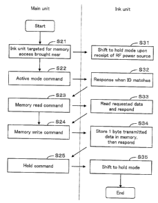
H. Details of memory acces ~ process
Figure I3 is a flow chart detailing the particulars of communication
between the ink unit (specifically, the memory element 311) and the printer
main unit (specifically, the transmitter/receiver 30) in the memory access
process. This flow chart corresponds to the details of the second procedure
shown in Figure 8 (steps s200 through s204 or steps s206 through s210).
When memory access is started, the carriage 20 first moves and stops
the ink unit targeted for memory access near the i~ransmitter/receiver 30
(step S21), thus moving the ink unit into hold mode M2 (step S31). The
transmitter/receiver 30 issues an active mode command including the ID in
_27_
PF04I19 Series Final
CA 02413597 2002-11-27
this state (step S22). V~Then the ID contained in the active mode coxmnand
matches the ID of the ink unit, the ink unit responds to the
transmitterlreceiver 30 and shifts to active mode 4 (step S32). As shown i.n
Figure 5(B), the active mode command includes all the in unit hD
information, thus allowing only one ink unit to shift to active mode M4. In
another embodiment, the ink unit may shift to active mode M4 without
responding to the transmitter/receiver 30 when the ID in the active mode
command matches the ID of the ink unit.
When the response from the ink unit is received, the
transmitterlreceiver 30 issues either a memory read command or memory
write command. In this example, a memory read command is first issued
(step S23). The memory command includes the cartridge ID, read start
address, and the read volume. When the ink unit receives the memory read
command, it reads the designated read volume data beginning from the
IS designated read start address, and responds to the transmitter/receiver 30
(step S33). The transmitterlreceiver 30 issues further memory write
commands as needed (step S24). The memory command includes the
cartridge ID, write address, and data to be written. When the ink unit
receives the memory write command, it writes data to the designated write
address and then responds to the transmitterlxeceiver 30 (step S34). When
the response is received, the transmitter/receiver 30 can check that the write
has been properly completed. When the memory access process for the ink
unit is completed, the transmitter/receiver 3D issues a hold command to the
ink unit, allowing it to shift to hold mode M2 (steps S25 and S35). High
frequency signals from the transmitter/receiver 30 may also be stopped to
stop the operation of the memory element 31I after step S34 without going
through steps S25 and 535.
In this way, when the memory access process is carried out, the
transmitter/receiver 30 first issues an active mode command including the
i0 total ID to allow only 1 ink unit to shift to active mode M4. As a result,
the
-28-
PF04I19 Series Final
CA 02413597 2002-11-27
i
memory access process can be carried out with just 1 ink unit, preventing
accidental memory access of other ink units.
In cases where the tr ansmitter/receiver 30 always limits the ink unit
which can shift into active n'zode 4 to one, the ID of the memory access
command (memory read command or memory write command) may be
entirely omitted, and just a specific portion of the ID may be included. ~n
advantage of including at least a portion of the ID in the memory access
command is that memory access will be more reliable. Including only a
specific portion of the ID in the memory access command can also increase
the reliability of memory access while also simplifying the command
structure.
Figure 14 is a flow chart detailing the reading process of the memory
element 311 (steps S23 and S33 in Figure 13). When the
transmitterlreceiver 30 issues a memory read command (step S41), the
memory element 311 (Figure 4) of the ink unit reads the designated number
of bytes of data from the memory cell 3117 (step S51). When no data can be
read at such times, the memory element 311 transmits a specific error code
indicating a data read failure (referred to as "total error code") to the
transmitter/receiver 30 (steps S52 and S53). When only some of the
designated number of bytes have been read, an error code indicating that
some of the data have not been read ("partial error code") is sent along with
the read data to the transmitter/receiver 30 (steps S54 and S55). When all
the designated bytes of data have been read, the data are sent to the
transmitter/receiver 30 (step S56). In another embodiment, the
transmitterlreceiver 30 may send a memory read command containing an ID,
and the memory element 311 of the ink unit may judge if the ID matches
that of the ink unit and carry out the processing of step S51 and thereafter
only when the IDs are the same. In this case, the memory element 311 may
not respond to the transmitter/receiver 30 if the IDs are different.
Because the transmitter/receiver 30 receives the response results,
-29-
PF04I19 Series Final
j CA 02413597 2002-11-27
the appropriate process can be run in accordance therewith (step S42). For
example, when a response including an erxor code is received, the same
n2emory read command can be reissued to allow the memory element 311
read the data. When a response including a partial error code is received,
just the received data is transmitted along with the partial error code to the
control circuit 50 in the main unit (Figure 6) to proceed to the next process.
Figure 15 is a flow chart detailing the processing of writing to the
memory element 311 (steps S24 and S34 in Figure 13). When the
transmitter/receiver 30 issues a memory write command (step 561), The
memory element 311 of the ink. unit writes data included in the memory
write command to the memory cell 3117 (step S71). When no data are
written, the memory element 311 sends a specific error code indicating the
data write failure to the transmitter/receiver 30 (steps S72 and S73). When
the data have been successfully written, a response indicating the successful
write is sent to the transmitter/receiver 30 (step S74). The
transmitterlreceiver 30 receives the response results, allowing the
appropriate process to be run in accordance therewith (step S62). For
example, when a response including an error code is received, the same
memory write command can be reissued to run the data writing process
again. In another embodiment, the transmitterlreceiver 30 may send a
memory write command containing an ID in the writing operation as in the
reading operation. In this case, the memory element 311 of the ink unit
may judge if the ID matches that of the ink unit and carry out the processing
of step S71 and thereafter only when the IDs are the same. The memory
'.5 element 311 may not respond to the transmitter/receiver 30 if the IDs are
different.
I. Variants in flow of communication between printer main unit and
memory element
Figure 16 is a .flow chart of another example of the flow of
communication between the memory elements and the printer main unit
-3fl-
PF04I19 Series Final
CA 02413597 2002-11-27
illustrated in Figure 8. When the power is on and none of the ink units
have been replaced, an active mode command is issued to run memory access
(second procedure) in the same manner as in Figure 8, alld will thus not be
described here again.
In the flow in Figure 16, when the power is on or an ink unit has
been replaced, the ink unit targeted for ID information check is first
determined (step 5304). For example, out of the 6 ink units INCI through
INC6, the first ink unit INCI is the target ink unit. The
transmitter/receiver 30 issues an active mode command to the target ink
unit (step 5305). The active mode command includes the ID information of
the 1St ink unit INC1 which have been registered in the control circuit 50
(Figure 6) of the printer main unit. When there is a response from the
target ink unit INC1 regarding the active mode command, the ID check of
the target ink unit INC1 is complete, The transmitter/receiver 30 then
moves from step 5306 to step 5309 to determine whether or not the process is
complete for all the cartridges. If it is determined that the process is not
complete in step 5309, the process returns to step 5304, and the next ink
unit INC2 is selected as the target ink unit.
In this way, in the routine involving steps 5304 through 5306 and
5309, the target ink unit is selected one at a time beginning from the Ist ink
unit, and the transmitter/receiver 30 issues an active mode command using
the registered ID information relating to the target ink unit. When there is
no response from the target ink unit, the ID information relating to the ink
unit must be checked, so the ID information is read (first procedure) and the
memory is accessed (second procedure), as illustrated in Figure 8, in steps
530'7 and 5308. In the memory access process, data on the amount of ink
remaining (amount of consumable component remaining) in the ink unit, for
example, can be read, and data for increasing by one the number of ink units
which have been replaced can be written. In this example, it is assumed
that data indicating the amount of ink remaining and the number of ink
31-
PF04I19 Series Final
CA 02413597 2002-11-27
units that have been replaced can be stored in the memory cell 311'7. As
such, the process from steps 5304 through 5308 is repeated until the ID
information relating to all the ink units have been checked (step 5309).
An advantage of the process procedure in Figure 16 is that the time
needed for the process as a whole can be shortened because the anti-collision
process is run only for ink units in which the ID information has not been
checked, with no need to run the anti-collision process for all of the ink
units
INC. The anti-collision process procedure itself can be simplified by
running the anti-collision process for all the ink units according to the
operations in Figure 9, even when ink units are replaced.
As will be apparent from the description above, the anti-collision
process (ID check in anti-collision mode M3) should be run on at least
replaced ink units after any of the ink units in the printer have been
replaced.
Depending on the device, a str ucture may be provided to determine
the position of the replaced ink unit after any of the ink units have been
replaced. In this type of device, the transmitter/receiver 30 may be brought
near just the replaced ink unit to check the ID in anti-collision mode,
without
any need for checking the ID of the other ink units.
When the device is powered on for the first time after being shipped,
the first procedure should be immediately started to check the ID, as in the
process procedure in Figure 8. The second time and thereafter that the
power is turned on after the device has been shipped, an active mode
command should be issued by the transmitter/receiver 30 to each ink unit, as
in the process procedure in Figure 16, to check the ID in anti-collision mode
M3 only in cartridges with no effective response.
J. Other variants
A printer device and the like relating to the present invention were
illustrated above based on some embodiments, but the above embodiments of
the invention were intended to facilitate an understanding of the invention,
-32-
PF04I19 Series Final
CA 02413597 2002-11-27
and do not limit the invention. Various modifications and improvements
are possible within the scope of the present invention, such equivalent
products naturally being included in the present invention
J1. Variant 1
The invention can be worked in the form of a computer system
comprising a computer main unit, display device connected to the computer
main unit, printer relating to the above embodiments connected to the
computer main body, input device such as mouse or keyboard provided as
needed, floppy disk drive device, and CD-ROM drive device. Such a
computer system will be a better system than conventional systems as such,
overall.
J2. Variant 2
The printer in the above embodiments may have the functions, or
some of the functions, of a computer main unit, display device, input device,
floppy disk drive device, and CD-ROM drive dives. For example, the printer
may have an image processor for processing images, a display for various
types of display, and a recording media insertion/removal component for
inserting and removing recording media on which are recorded image data
taken by means of digital cameras or the like.
J3. Variant 3
Although an ink jet printer 10 employing cut paper as the printing
object was used as the printer in the above embodiments, printing objects
other than cut paper, such as roll paper, can also be used. The printer is
also not limited to color ink jet printers. For example, monochromatic
printers, laser printers, and faxes are applicable, provided that the printer
is
capable of printing such printing objects.
J4. Variant 4
The memory element used in the above embodiments comprised a
non-contact IC chip, a resonance capacitor formed by etching a metal film,
and a flat antenna coil, but is not Limited to such a structure, provided that
-33-
PF04I19 Series Final
CA 02413597 2002-11-27
the structure is capable of recording data. For example, a resonance
capacitor may be connected to the outside of the memory element,
J5. Variant 5
In the above embodiments, three modes including hold mode M2,
anti-collision mode M3, and active mode M4 were used as modes during the
operation of the memory element, but the memory element 311 may also
have other modes. For example, hold mode M2 can be divided into a
plurality of hold sub-modes. More specifically, the reception of a high
frequency signal from the transmitter/receiver 30 can result in a shift to a
first hold sub-mode, and the reception of a specific shift command in the
first
hold sub-mode can result in a shift to a second hold sub-mode. At that time.
when the memory element receives an active mode command while in the
first hold sub-mode, it should move immediately to the active mode M4, and
when it receives an anti-collision start command while in the second hold
sub-mode, it should move immediately to anti-collision mode M3. In this
structure, an anti-collision process malfunction will result in a return to
the
second hold sub-mode, while the receipt of a hold command will r esult in a
shift from the active mode M4 to the first hold sub-mode. The use of such a
hold mode structure can limit the shifts between operating modes, and can
thus prevent accidental shifts to inappropriate operating modes. That is,
the advantage is the ability to ensure more reliable shifts between operating
modes.
However, the memory element does not need to have a hold mode.
For example, the memory element can be designed to shift immediately to
active mode when power is generated upon receipt of a high frequency signal
from the transmitter/receiver. The memory element can also be designed to
shift from a specific mode other than anti-collision mode or active mode to
active mode without going through anti-collision mode. That is, the
memory element (memory circuit) of the present invention may generally be
able to shift from a specific state that is not in anti-collision mode to
active
- 34 -
PF04I19 Series Final
CA 02413597 2002-11-27
mode without going through anti-collision mode. However, it is preferable
that the memory element shifts to active mode upon receipt of an active
mode command including the ink unit ID. Furthermore, the memory
element may preferably shift fr om hold mode to active mode when receiving
a read command or write command containing the ink unit ID in hold mode,
so as to carry out reading or writing operation.
J6. Variant 6
The embodiments above illustrated a printer in which ink units can
be installed, but the present invention is generally applicable to a variety
of
devices in which cartridges with consumable components can be installed.
The device does not need to be one in which a plurality of cartridges with a
consumable component can be installed, but should allow one or more
cartridges with a consumable component to be installed. In the above
embodiments, cartridges with a consumable component were moved along
with the carriage (cartridge holder), but the transmitter/receiver may
alternatively be moved. The positional relationship between the
transmitter/receiver and cartridge may also be fixed, with neither the main
unit transmitter/receiver or cartridge being moved.
J7. Variant 7
In the above embodiments, the transmitter/receiver 30 and ink unit
were within a specific distance of no more than about 30 mm of each other
while communicating, but the outer surface of the cartridge and the
transmitterlreceiver may generally be in contact during communication.
That is, the transmitter/receiver and cartridge should be capable of non-
contact communication while adjacent to each other. In the present
Specification, the expression concerning "non-contact" between the
transmitter/receiver and cartridge means that the electric circuitry of the
transmitter/receiver and the electrical circuitry of the cartridge are not
connected by electrical wiring. The outer surfaces may be in contact with
each other.
-35-
PF04I19 Series Final
CA 02413597 2002-11-27
J8. Variant 8:
In the above embodiments, the transmitter/receiver 30 allowed two
ink units to simultaneously shift into hold mode, but the
transmitterlreceiver should generally have the capacity of simultaneously
moving two or more cartridges to hold Triode. However, the
transmitter/receiver should not have the capacity of simultaneously moving
all of the maximum number of cartridges which can be mounted into hold
mode. That is because it would be difficult to distinguish the position of
each cartridge in the anti-collision process (ID check process) if the
transmitter/receiver had the capacity to simultaneously move all the
cartridges into hold mode. In that sense, it is particularly desirable for the
transmitter/receiver to have the capacity of simultaneously moving one or
two cartridges into hold mode.
Although the present invention has been described and illustrated in
detail, it is clearly understood that the same is by way of illustration and
example only and is not to be taken by way of limitation, the scope of the
present invention being limited by the terms of the appended claims.
Paragraphs of advantage
1. A device in which a cartridge containing a consumable
component can be installed, the device comprising:
a cartridge holder in which one or more cartridges containing a
consumable component can be mounted and
a transmitter/receiver capable of non-contact communication while
proximate to the carte idge,
the cartridge having a memory circuit including an antenna capable
of non-contact communication while proximate to the transmitter/receiver, a
memory for storing an ID of the car tridge and data relating to the
consumable component, and a controller for controlling communication with
the transmitter/x°eceiver and for controlling access to the memory,
the memory circuit having an anti-collision mode in which the
-36-
PF04I19 Series Final
CA 02413597 2002-11-27
transmitter/receiver can check the ID of the cartridge, and an active mode
permitting memory access upon reception of a memory access command from
the transmitter/receivex,
the memory circuit being capable of shifting from a specific state
which is not in anti-collision mode to active mode without passing through
the anti-collision mode.
2. A device according to Par agraph 1, whey ein the memory circuit
shifts to the active mode without passing through the anti-collision mode
upon receipt of an active mode command including the ID of the cartridge
while not in the anti-collision mode.
3. A device according to Paragraph 1 or 4, wherein the memory
circuit shifts to the active mode after the ID has been checked in the anti-
collision mode.
4. A device according to Paragraph 3, wherein the memory circuit
further comprises a hold mode in which the memory circuit cannot receive a
memory access commands, and
the memory circuit shifts to the active mode upon receipt of the
active mode command when in the hold mode.
5. A device according to Paragraph 4, wherein the memory circuit
further comprises an electrical power generating component for generating
electrical power output for the memory circuit in response to high frequency
radio signals received from the transmitter/receiver,
the hold mode including a first hold sub-mode in which electrical
power output is generated in the memory circuit in response to the high
frequency radio signals received from the tx~ansmitter/receiver, and a second
hold sub-mode to which the memory circuit shifts upon receiving a
predetermined shift command from the transmitter/receiver in the first hold
sub-mode,
the memory circuit shifts directly to the active mode upon receipt of
the active mode command when in the first hold sub-mode, and
- 3'l -
PF04I19 Series Final
CA 02413597 2002-11-27 -
the memory circuit shifts directly to the anti-collision mode upon
receipt of an anti-collision start command when in the second hold sub-mode.
6. A device according to Paragraph 4 or ~, wherein the device
carries out a full cartridge anti-collision process in which the one or more
cartridges which have been installed are sequentially allowed one at a time
to approach the transmitterlreceiver when the device is first powered on
after being shipped, and in which the ID of each cartridge is checked in the
anti-collision mode while a target cartridge targeted for ID check is
positioned such that the transmitter/receiver is possible to distinguish the
position of the target cartridge.
7. A device according to Paragraph 6, wherein the full cartridge
anti-collision process is carried out each time the device is powered on.
8. A device actor ding to Par agraph 6, wherein the active mode
command is transmitted by the transmitter/receiver to each cartridge when
the device is powered on for the second time or thereafter after being
shipped,
and the ID is checked in the anti-collision mode only for cartridges which
have not made an effective response to the active mode command.
9. A device according to any of Paragraphs 4 through 6, wherein
after any of the cartridges installed in the device have been replaced, the ID
of at least the replaced cartridge is checked in the anti-collision mode.
10. A device according to Paragraph 9, further comprising a drive
mechanism capable of moving one of the cartridge holder and the
transmitter/receiver to bring the cartridges and transmitter/receiver
proximate to each other, and
the full anti-collision process is carried out, in which the one or more
cartridges which have been installed are sequentially allowed one at a time
to approach the transmitter/receiver after any of the cartridges installed in
the device have been replaced, and the ID of each cartridge is checked while
the transmitter/receiver is possible to distinguish the position of the target
cartridges targeted for ID check in the anti-collision mode.
-38-
PF04I19 Series Final
CA 02413597 2002-11-27
ii. A device according to Paragraph 9, further comprising a drive
mechanism capable of moVIIlg one of the cartridge holder and the
transmitter/receiver to bring the cartridges and transmitter/receiver
proximate to each other, and
the transmitter/receiver approaches only the replaced cartridges
after any of the cartridges installed in the device have been replaced, so as
to
check the ID in the anti-collision mode without checking the ID of the other
cartridges.
12. A device according to Paragraph 11, wherein the active mode
command is transmitted near each cartridge installed in the device after any
of the cartridges in the device have been replaced, and the ID is checked in
the anti-collision mode only for cartridges which have not made an effective
response.
13. A device actor ding to any of Paragraphs 4 through 12, wherein
the transmitter/receiver is capable to simultaneously shift two or more
cartridges into the hold mode, but is not capable to simultaneously shift all
of the maximum number of cartridges which can be installed in the device
into the hold mode.
14. A cartridge containing a consumable component, comprising:
a memory circuit including an antenna capable of non-contact
communication while proximate to an exterior transmitter/receiver, a
memory for storing an ID of the cartridge and data relating to the
consumable component, and a controller for controlling communication with
the tr ansmitter/receiver and for controlling access to the memory,
the memory circuit having an anti-collision mode in which the
transmitter/receiver can check the ID of the cartridge, and an active mode
permitting memory access upon reception of a memory access command from
the transmitter/receiver,
the memory circuit being capable of shifting from a specific state
which is not in anti-collision mode to active mode without passing through
-39-
PF04I19 Series Final
CA 02413597 2002-11-27
the anti-collision mode.
15. A cartridge according to Paragraph 14, wherein the memory
circuit shifts to the active mode without passing through the anti-collision
mode upon receipt of an active mode command including the ID of the
cartridge while not in the anti-collision mode.
16. A cartridge accor ding to Par agraph 14 or 15, wherein the
memory circuit shifts to the active mode after the ID has been checked in the
anti-collision mode.
17. A cartridge according to Paragr aph 16, wherein the memory
circuit further comprises a hold mode in which the memory circuit cannot
receive a memory access commands, and
the memory circuit shifts to the active mode upon receipt of the
active mode command when in the hold mode.
18. A cartridge according to Paragraph 17, wherein the memory
circuit further comprises an electrical power generating component for
generating electrical power output for the memory circuit in response to high
frequency radio signals received from the transmitter/receiver,
the hold mode including a first hold sub-mode in which electrical
power output is generated in the memory circuit in response to the high
frequency radio signals received from the transrnitter/receiver, and a second
hold sub-mode to which the memory circuit shifts upon receiving a
predetermined shift command from the transmitterlreceiver in the first hold
sub-mode,
the memory circuit shifts directly to the active mode upon receipt of
the active mode command when in the first hold sub-mode, and
the memory circuit shifts directly to the anti-collision mode upon
receipt of an anti-collision start command when in the second hold sub-mode.
19. A cartridge according to any of Paragraphs 14 through 18,
wherein an anti-collision start command for shifting the memory circuit
includes only a portion of the ID which can be commonly assigned to a
-40-
PF04I19 Series Final
CA 02413597 2002-11-27
plurality of cartridges, and
the memory circuit can undergo an anti-collision process at the same
time as other memory circuits of other cartridges when the portion of the ID
included in the anti-coliision start command is the same with the
corresponding portion of ID in the memory circuit.
20. A cartridge according to Paragraph 19, wherein the memory
circuit is capable of undergoing the anti-collision process at the same time
as
other memory circuits of other cartridges only when the antennas of each
cartridge and the antenna of the transmitter/receiver are within
approximately 30 mm of each other.
21. A cartridge according to Paragraph 14, wherein the memory
access command includes a read command with the entirety of the ID of the
cartridge and a write command with the entirety of the ID of the cartridge.
22. A cartridge according to Paragraph 14, wherein the memory
access command includes a read command with only a specific portion of the
ID of the cartridge and a write command with only a specific portion of the
ID of the cartridge.
23. A cartridge according to Paragraph 21 or 22, wherein the read
command includes a read start address and quantity of data to be read, and
the memory circuit reads data from the memory according to the read
command to supply the read data to the transmitter/receiver.
24. A cartridge according to Paragraph 23, wherein the memory
circuit sends the read data and an error code indicating that a read error has
occurred back to the transmitter/receiver when only a portion of an amount
of read data requested by the read command has been read.
2~. A cartridge according to any of Paragraphs 21 through 24,
wherein the write command includes a write address and a predetermined
amount of data, and
the memory circuit writes the predetermined amount of data
according to the write command and then notifies the transmitter/receiver
-41-
PF04I19 Series Final
CA 02413597 2002-11-27
that the data has been written.
26. A cartridge according to Paragraph 14, wherein the memory
circuit generates power from high frequency radio signals and shifts to the
hold mode upon reception of the high frequency radio signals transmitted by
the transmitter/receiver antenna within a predetermined distance of no
more than approximately 30 mm of the antenna of the memory circuit, but
does not operate when the transmitter/receiver antenna is not within the
predetermined distance from the antenna of the memory circuit.
2'l. A cartridge according to Paragraph 14, wherein alI commands
which the memory circuit is capable of receiving include at least a portion of
the ID, and
the memory runs operations in response to a command only when the
at least a portion of the ID in the received command is the same with the
corresponding ID portion of the cartridge.
28. A cartridge containing a consumable component and having an
element capable of storing data, a plurality of cartridges being mountable in
a cartridge support member of a device having a device main unit, the
element being subject to data read or data write operation through non-
contact communication between the element and communication means
provided in the device main unit, the cartridge being characterized in that:
the device main unit is capable of carrying out a first procedure in
which the communication means communicates with the element of each
cartridge to read ID information stored in the element, and a second
procedure in which the communication means communicates with the
element of each cartridge disposed on the cartridge support member while
distinguishing each element based on the ID informai;ion that has been read
and
the second procedure is run without the first procedure being run if
the ID information stored in the element of a particular cartridge has
already been properly read by the device main unit when the communication
-42-
PF04I19 Series Final
CA 02413597 2002-11-27
._
means starts communicating with the element, so that the element and the
communication means communicate with each other while the element is
distinguished based on the ID information.
29. A printer comprising a plurality of ink units equipped with
elements capable of storing data, an ink unit support member for supporting
the plurality of ink units, and communication means for reading or writing
data by non-contact communication with the elements, the printer having:
a first procedure in which the communication means communicates
with the element of each ink unit to read ID information stored in the
element, and
a second procedure in which the communication means
communicates with the element of each ink unit supported by the ink unit
support member while distinguishing the element based on the ID
information that has been read,
wherein the second procedure is run without the first procedure
being run if the ID information stored in the element of a particular ink unit
has already been properly read when the communication means starts
communicating with the element, so that the communication means
communicates with the element.
30. A printer according to Paragraph 29, wherein the ink units are
detachable from the ink unit support member.
31. A printer according to Paragraph 30, wherein after the ID
information stored in the elements in each ink unit has been read upon
execution of the first procedure, the second procedure is run without the
first
procedure being run as long as power-off and power-on of the printer are not
carried out and none of the ink units has been replaced, allowing the
communication means to communicate with the elements.
32. A printer according to any of Paragraphs 29 through 31,
wherein the ID information is element-specific data stored in the element
before the element is attached to the ink unit.
-43-
PF04I19 Series Final
CA 02413597 2002-11-27
a
33. A printer according to any of Paragraphs 29 through 32,
wherein the ink unit support member is movable, and
the element provided in each ink unit receives power from the printer
main unit only when brought proximate to the communication means by the
movement of the ink unit support member.
34. An ink unit having an element capable of storing data, a
plugality of ink units being mountable in an ink unit support member of
printer having a printer main unit, the element being subject to data read or
data write operation through non-contact communication between the
element and communication means provided in the printer main unit, .
when ein the ink unit is character ized in that:
the printer main unit is capable of carrying out a first procedure in
which the communication means communicates with the element of each ink
unit to read ID information stored in the element, and a second procedure in
which the communication means communicates with the element of each ink
unit disposed on the ink unit support member while distinguishing each
element based on the ID information that has been read and
the second procedure is run without the first procedure being run if
the ID information stored in the element of a particular ink unit has already
been properly read by the printer main unit when the communication means
starts communicating with the element, so that the element and the
communication means communicate with each other as the element is
distinguished based on the ID information.
35. An ink unit according to Paragraph 34, wherein the ink unit is
detachable from the ink unit support member.
36. An ink unit according to Paragraph 34 or 35, wherein the ID
information are element-specific data stored in the elements before the
elements are attached to the ink units.
37. An ink unit according to any of Paragraphs 34 through 36,
wherein the ink unit support member is movable, and
44 -
PF04I19 Series Final
CA 02413597 2002-11-27
~ :i
the element of the ink unit receives power from the printer main unit
only when brought proximate to the communication means by the movement
of the ink unit support member.
38. An ink unit according to Paragraph 34, wherein the ID
information comprises manufacturing data of the ink units.
39. An ink unit according to Paragraph 38, wherein the
manufacturing data include data for specifying the year in which the ink
unit was manufactured.
40. An ink unit according to Paragraph 38 or 39, wherein the
manufacturing data include data for specifying the month in which the ink
unit was manufactured.
41. An ink unit according to any of Paragraphs 38 through 40,
wherein the manufacturing data includes data for specifying the day on
which the ink unit was manufactured.
42. An ink unit according to any of Paragraphs 38 through 41,
wherein the manufacturing data includes data for specifying a location
where the ink unit was manufactured.
43. An ink unit according to any of Paragraphs 38 through 42,
wherein the element comprises a veritable area where the printer main unit
can write data and a nonwritable area where the printer main unit cannot
write data, and the manufacturing data are stored in the nonwritable area.
44. An ink unit according to any of Paragraphs 38 through 43,
wherein a plurality of the ink units are mountable on the unit support
member provided in the printer main unit, the ID information stored in the
elements of the plurality of the ink units is read in a non-contact manner by
the communication means provided in the printer main unit, and relation
between a layout sequence of the ink units on the ink unit support member
and the ID information stored in the elements provided in the ink units is
specified by the printer main unit.
45. An element which is capable of storing data and is provided in
PF04I19 Series Final
CA 02413597 2002-11-27
1
an ink unit, a plurality of which are mountable on an ink unit support
member of a printer having a printer main unit, the element being subject to
data read or data write operation through non-contact communication
between the element and communication means provided in the printer
main unit, the element being characterized in that:
the printer main unit is capable of carrying out a first procedure in
which the communication means communicates with the element of each ink
unit to read ID information stored in the element, and a second procedure in
which the communication means communicates with the element of each ink
IO unit disposed on the ink unit support member while distinguishing the
element based on the ID information that has been read and
the second procedure is run without the first procedure being run if
the ID information stored in the element of a particular ink unit has already
been properly read by the printer main unit when the communication means
starts communicating with the element, so that the element and the
communication means communicate with each other as the element is
distinguished based on the ID information.
46. A computer system comprising:
a computer main unit
a display connected to the computer main unit> and
a printer connected to the computer main unit, the printer
comprising a plurality of ink units equipped with elements capable of staring
data, an ink unit support member for supporting the plurality of ink units,
and communication means for reading or writing data by non-contact
communication with the elements,
the printer being capable of carrying out a first procedure in which
the communication means communicates with the element of each ink unit
to read ID information stored in the element, and a second procedure in
which the communication means communicates with the element of each ink
unit supported by the ink unit support member while distinguishing the
-46-
PF04I19 Series Final
CA 02413597 2002-11-27
element based on the ID information that has been read,
wherein the second procedure is run without the first procedure
being run if the ID information stored in the element of a particular ink unit
has already been properly read when the communication means starts
communicating with the element, so that the communication means
communicates with the element.
47. A printer comprising a plurality of ink units equipped with
elements capable of storing data, an ink unit support member for supporting
the plurality of ink units, and communication means for reading or writing
data by non-contact communication with the elements, the printer having:
a first procedure in which the communication means communicates
with the element of each ink unit to read ID information stored in the
element, and
a second procedure in which the communication means
communicates with the element of each ink unit supported by the ink unit
support member while distinguishing the element based on the TD
information. that has been read,
wherein after the ID information stored in the elements in each ink
unit has been read upon execution of the first procedure, the second
procedure is run without the first procedure being run as long as power-off
and power-on of the printer are not carried out and none of the ink units has
been replaced, allowing the communication means to communicate with the
elements
the ink units are detachable from the ink unit support member
the ID information is element-specific data stored in the element
before the element is attached to the ink unit, and
the ink unit support member is movable, and the element provided in
each ink unit receives power from the printer main unit only when brought
proximate to the communication means by the movement of the ink unit
support member.
-47-
PF04I19 Series Final
CA 02413597 2002-11-27
48. A method for identifying a cartridge containing a consumable component
and having an element for storing data, a plurality of the cartridges being
mountable in a
cartridge support member of a device having a device main unit, the element
being
subject to data read or data write operation through non-contact communication
between
the element and a communication device provided in the device main unit,
comprising
the steps of:
performing, using the device main unit, a first procedure in which the
communication device communicates with the element of each of the cartridges
to read
ID information stored in the element; and
performing, using the device main unit, a second procedure in which the
communication device communicates with the element of each of the cartridges
disposed on the cartridge support member while distinguishing each of the
elements
based on the ID information that has been read,
wherein the second procedure is run without the first procedure being run if
the
ID information stored in the element of a particular cartridge has already
been properly
read by the device main unit when the communication device starts
communicating with
the element, so that the element and the communication device communicate with
each
other while the element is distinguished based on the ID information.
49. A method of identifying a plurality of ink units in a printer,
comprising the steps of:
providing the printer, the printer having a plurality of ink units equipped,
respectively, with elements capable of for storing data, an ink unit support
member for
supporting the plurality of ink units, and a communication device for reading
or writing
data by non-contact communication with the elements;
performing a first procedure in which the communication device
communicates with the element of each said ink unit to read ID information
stored in
the element; and
performing a second procedure in which the communication means
device communicates with the element of each said ink unit supported by the
ink unit
_ 48 _
PF04I19 Series Final
- CA 02413597 2005-05-30
support member while distinguishing the element based on the ID information
that has
been read,
wherein the second procedure is run without the first procedure being run
if the ID information stored in the element of a particular said ink unit has
already been
properly read when the communication means device starts communicating with
the
element, so that the communication means device communicates with the element.
50. A method according to Paragraph 49, wherein the ink units are
detachable from the ink unit support member,
51. A method according to Paragraph 50, wherein after the ID
information stored in the elements in each of the ink units has been read upon
execution
of the first procedure, the second procedure is run without the first
procedure being run
as long as power-off and power-on of the printer are not carried out and none
of the ink
units has been replaced, allowing the communication device to communicate with
the
_._ _ ____e~m~s.-___________________________.__ __ _ _ _ .- __ _-_ _ _ _ ._.._
.__ _
52. A method according to Paragraph 49, wherein the ID information is
element-specific data stored in the element before the element i s attached to
the ink unit.
53. A method according to Paragraph 49, wherein the ink unit support
member is movable, and
the element provided in each of the ink units receives power from the
printer only when brought proximate to the communication device by movement of
the
ink unit support member.
54. A method of identifying a plurality of ink units in a printer,
comprising the steps of:
-49-
PF04I19 Series Final
CA 02413597 2002-11-27
providing the printer, the printer having an ink support member and a
printer main unit having a communication device;
providing the ink units, each said ink unit having an element for storing
data, the ink units being mounted in the ink unit support member, the element
being
subject to a data read operation or a data write operation through non-contact
communication between the element and the communication device;
performing a first procedure in which the communication device
communicates with the element of each said ink unit to read ID information
stored in
the element; and
performing a second procedure in which the communication device
communicates with the element of each said ink unit disposed on the ink unit
support
member while distinguishing each said element based on the ID information that
has
been read,
wherein the second procedure is run without the first procedure being run
if the ID information stored in the element of a particular said ink unit has
already been
properly read by the printer main unit when the communication device starts
communicating with the element, so that the element and the communication
means
device communicate with each other as the element is distinguished based on
the ID
information.
55. A method according to Paragraph 54, wherein the ink unit is
detachable from the ink unit support member.
-50-
PF04I19 Series Final
CA 02413597 2002-11-27
56. A method according to Paa~agraph 54, wherein the ID information
are element-specific data stored in tle elements before the elements are
attached to the
ink units.
57. A method according to Paragraph 54, wherein the ink unit support
member is movable, and
the element of the ink unit receives power from the printer main unit only
when brought proximate to the communication device by movement of the ink unit
support member.
58. A method according to Paragraph 54, wherein the ID information
comprises manufacturing data for the ink units.
59. A method according to Paragraph 58, wherein the manufacturing
data include data for specifying a year in which the ink unit was
manufactured.
60. A method according to Paragraph 58, wherein the manufacturing
data include data for specifying a month in which the ink unit was
manufactured.
61. A method according to Paragraph 58, wherein the manufacturing
data includes data for specifying a day on which the ink unit was
manufactured.
62. A method according to Paragraph 58, wherein the manufacturing
data includes data for specifying a location where the ink unit was
manufactured.
_~1_
PF04119 Series Final
CA 02413597 2002-11-27
63. A method according to Paragraph 58, wherein the element
comprises a writable area where the punter main unit can write data and a
nonwritable
area where the printer main unit cannot write data, and the manufacturing data
are stored
in the nonwi-itable area.
b4. A method according to Paragraph 58, wherein a plurality of the ink
units are mounted on the unit support member provided in the printer main
unit, the ID
infornation stored in the elements of the ink units is read in a non-contact
manner by
the communication device provided in the printer main unit, and a relationship
between
a.layout sequence of the ink units on the ink unit support member and the ID
I O information stored in the elements provided in the ink units is specified
by the printer
mam unit.
65. A method of identifying a plurality of ink units in a printer,
comprising the steps of
providing the plurality of ink units respectively equipped with elements
I S for storing data,
providing the printer, the printer having a movable ink unit support
member for supporting the plurality of ink units, the ink units being
detachable from the
ink unit support member, and a communication device for reading or writing
data by
non-contact communication with the elements, and the element provided in each
said
20 ink unit receives power from the printer only when brought proximate to the
communication device by a movement of the ink unit support member;
-52-
PF04i19 Series Final
CA 02413597 2002-11-27
performing a first procedure in which the communication lneans device
communicates with the element of each said ink unit to read ID information
stored in
the element, wherein the ID information is element-specific data stored in the
element
before the element is attached to the ink unit, and
performing a second procedure in which the communication device
communicates with the element of each said ink unit supported. by the ink unit
support
member while distinguishing the element based on the ID information that has
been
read,
wherein, after the ID information stored in the elements in each said ink unit
has been
read upon execution of the first procedure, the second procedure is run
without the fir st
procedure being run as long as power-off and power-on of the printer are not
carried out
and none of the ink units has been replaced, allowing the communication device
to
communicate with the elements.
-53-
PF04I19 Series Final