Note: Descriptions are shown in the official language in which they were submitted.
CA 02414124 2002-12-12
Antenna With Near-Field Radiation Control
FIELD OF THE INVENTION
This invention relates generally to the field of antennas. More specifically,
an antenna is
provided that is particularly well-suited for use in wireless mobile
communication devices,
generally referred to herein as "mobile devices", such as Personal Digital
Assistants, cellular
telephones, and wireless two-way email communication devices.
BACKGROUND OF THE INVENTION
Many different types of antenna for mobile devices are known, including helix,
"inverted
F", folded dipole, and retractable antenna structures. Helix and retractable
antennas are typically
installed outside of a mobile device, and inverted F and folded dipole
antennas are typically
embedded inside of a mobile device case or housing. Generally, embedded
antennas are
preferred over external antennas for mobile devices for mechanical and
ergonomic reasons.
Embedded antennas are protected by the mobile device case or housing and
therefore tend to be
more durable than external antennas. Although external antennas may physically
interfere with
the surroundings of a mobile device and make a mobile device difficult to use,
particularly in
limited-space environments, embedded antennas present fewer such challenges.
However,
established standards and limitations on near-field radiation tend to be more
difficult to satisfy
for embedded antennas without significantly degrading antenna performance.
1
CA 02414124 2005-04-O1
SUMMARY
According to an aspect of the invention, an antenna comprises a first
conductor
section electrically coupled to a first feeding point, a second conductor
section electrically
coupled to a second feeding point, and a new-field radiation control structure
adapted to
control characteristics of near-field radiation generated by the antenna.
In accordance with another aspect of the invention, a wireless mobile
communication device comprises a receiver configured to receive communication
signals,
a transmitter configured to transmit communication signals, and an antenna
having a first
feeding point and a second feeding point connected to the receiver and the
transmitter.
The antenna comprises a first conductor section connected to a first feeding
point, a
parasitic element positioned adjacent the first conductor section and
configured to control
characteristics of near-field radiation generated by the first conductor
section, and a
second conductor section connected to the second feeding point and comprising
a diffizser
configured to diffuse near-field radiation into a plurality of directions.
In accordance with another aspect of the invention, there is provided an
antenna
comprising a first conductor section electrically coupled to a first feeding
point; a second
conductor section electrically coupled to a second feeding point; and a near-
field radiation
control structure adapted to control characteristics of near-field radiation
generated by the
antenna; wherein the near-field radiation control structure comprises a
parasitic element
positioned adjacent the first conductor section; wherein the first conductor
section
comprises a folded conductor having a first arm electrically coupled to the
first feeding
point and a second arm electrically coupled to the first arm, and wherein the
parasitic
element comprises a conductor positioned between the first arm and the second
arm.
In yet a fizrther aspect, there is provided an antenna comprising a first
conductor
section electrically coupled to a first feeding point; a second conductor
section electrically
coupled to a second feeding point; and a near-field radiation control
structure adapted to
control characteristics of near-field radiation generated by the antenna;
wherein the near-
field radiation control structure comprises a diffuser having multiple
conductor sections
extending in different directions to diffuse near-field radiation into
multiple directions
perpendicular to the conductor sections of the diffuser.
Another aspect of the invention provides an antenna comprising a first
conductor
section electrically coupled to a first feeding point; a second conductor
section electrically
coupled to a second feeding point; and a near-field radiation control
structure adapted to
2
CA 02414124 2005-04-O1
control characteristics of near-field radiation generated by the antenna;
wherein the near-
field radiation control structure comprises a parasitic element positioned
adjacent the first
conductor section; wherein the second conductor section comprises a folded
conductor
having a first arm electrically coupled to the second feeding point and a
second arm
electrically coupled to the first arm, and wherein the near-field radiation
control structure
further comprises a pair of diffusers respectively connected in the first and
second arms of
the second conductor section to diffused near-field radiation generated in the
second
conductor section into multiple directions.
A yet further aspect of the invention provides a wireless mobile communication
device comprising a receiver configured to receive communication signals; a
transmitter
configured to transmit communication signals; and an antenna having a first
feeding point
and a second feeding point connected to the receiver and the transmitter, the
antenna
comprising: a first conductor section connected to the first feeding point; a
parasitic
element positioned adjacent the first conductor section and configured to
control
characteristics of near-filed radiation generated by the first conductor
section; and a
second conductor section connected to the second feeding point and comprising
a diffuser
configured to diffuse near-field radiation into a plurality of directions.
Further features and aspects of the invention will be described or will become
apparent in the course of the following detailed description.
BRIEF DESCRIPTION OF THE DRAWINGS
Fig. 1 is a top view of an antenna according to a first embodiment of the
invention.
Figs. 2(a)-2(f) are top views of alternative parasitic elements.
Fig. 3 is a top view of an alternative diffusing element.
Fig. 4 is an orthogonal view of the antenna shown in Fig., 1 mounted in a
mobile
device; and
2a
CA 02414124 2002-12-12
Fig. 5 is a block diagram of a mobile device.
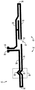
DETAILED DESCRIPTION
Fig. 1 is a top view of an antenna according to a first embodiment of the
invention. The
antenna 10 includes a first conductor section 12 and a second conductor
section 14. The first and
second conductor sections 12 and 14 are positioned to define a gap 16, thus
forming an open-
loop structure known as an open folded dipole antenna.
The antenna IO also includes two feeding points 18 and 20, one connected to
the first
conductor section 12 and the other connected to the second conductor section
14. The feeding
points 18 and 20 are offset from the gap 16 between the conductor sections 12
and 14, resulting
in a structure commonly referred to as an "offset feed" open folded dipole
antenna. The feeding
points 18 and 20 are configured to couple the antenna 10 to communications
circuitry. For
example, the feeding points 18 and 20 couple the antenna 10 to a transceiver
in a mobile device,
as illustrated in Fig. 4 and described below.
Operating frequency of the antenna 10 is determined by the electrical length
of the first
conductor section 12, the second conductor section 14, and the position of the
gap 16 relative to
the feeding points 18 and 20. For example, decreasing the electrical length of
the first conductor
section 12 and the second conductor section 14 increases the operating
frequency band of the
antenna 10. Although the conductor sections 12 and 14 are electromagnetically
coupled through
the gap 16, the first conductor section 12 is the main radiator of the antenna
10.
As those familiar with antenna design will appreciate, the second conductor
section 14 in
the folded dipole antenna 10 is provided primarily to improve the efficiency
of the antenna 10.
Environments in which antennas are implemented are typically complicated. The
second
3
CA 02414124 2002-12-12
conductor section 14 significantly increases the overall size of the antenna
10 and thus reduces
the antenna dependency on its surrounding environment, which improves antenna
efficiency.
Operation of an offset feed open folded dipole antenna is well known to those
skilled in
the art. The conductor sections 12 and 14 are folded so that directional
components of far-field
radiation, which enable communications in a wireless communication network,
generated by
currents in different parts of the conductor sections interfere constructively
in at least one of the
conductor sections. For example, the first conductor section 12 includes two
arms 22 and 24
connected as shown at 26. Current in the first conductor section 12 generates
both near- and far-
field radiation in each of the arms 22 and 24. The arms 22 and 24 are sized
and positioned, by
adjusting the location and dimensions of the fold 26, so that the components
of the generated far-
field radiation constructively interfere, thereby improving the operating
characteristics of the
antenna 10. The location of the gap 16 in the antenna 10 is adjusted to
effectively tune the phase
of current in the arms 22 and 24, to thereby improve constructive interference
of far-field
radiation generated in the first conductor section 12. Since the first
conductor section 12 is the
primary far-field radiation element in the antenna 10, maintaining the same
phase of current in
the arms 22 and 24 also improves antenna gain.
The first and second conductor sections 12 and 14 generate not only far-field
radiation,
but also near-field radiation. From an operational standpoint, the far-field
radiation is the most
important for communication functions. Near-field radiation tends to be
confined within a
relatively limited range of distance from an antenna, and as such does not
significantly contribute
to antenna performance in communication networks. As described briefly above,
however,
mobile devices must also satisfy various standards and regulations relating to
near-field
radiation.
4
CA 02414124 2002-12-12
Although antennas generate near-field radiation in addition to desired far-
field radiation,
near-field radiation tends to be much more difficult to analyze in antenna
design. Far-field
radiation patterns and polarizations for many types of antenna are known and
predictable,
whereas strong near-field radiation effects can be localized in an antenna.
Generally, the near-
field region of an antenna is proportional to the largest dimension of the
antenna. However,
simulation and other techniques that are often effective for predicting far-
field radiation
characteristics of an antenna have proven less reliable for determining near-
field radiation
patterns and polarizations.
A common scheme for reducing strong near-field radiation to acceptable levels
involves
installing a shield in a mobile device to at least partially block near-field
radiation. Localized
shielding required to reduce strong near-field radiation to acceptable levels
also have more
significant effects on far-field radiation, and thereby degrade the
performance of the antenna. In
accordance with an aspect of the invention, the antenna 10 includes near-field
radiation control
structures. These structures, labeled 34 and 36 in Fig. 1, provide another
control mechanism for
localized near-field radiation.
The structure 34 is a parasitic element comprising a conductor and a
connection that
electrically couples the conductor to the first conductor section of the
antenna 10. The length of
the conductor in a parasitic element determines whether the parasitic element
is a director or
deflector. As those skilled in the art will appreciate, a parasitic deflector
deflects near-field
radiation. Although the near-field radiation pattern changes with a parasitic
director, the
direction of energy of such near-field radiation can be enhanced toward the
direction of a
parasitic director, generally to a greater degree than for a parasitic
deflector. Near-field radiation
5
CA 02414124 2002-12-12
is deflected or directed by the parasitic element 34 to reduce near-field
radiation in particular
directions.
As described above, near-field radiation tends to be more difficult to predict
and analyze
than far-field radiation. For far-field radiation, the length of a parasitic
element is dependent
upon the wavelength of the radiation to be directed or deflected, which is
related to the operating
frequency band of an antenna. Parasitic elements having a length greater than
half the
wavelength act as deflectors, and shorter elements act as directors. However,
near-field radiation
characteristics are also affected by mutual coupling between elements of an
antenna. As such,
near-field radiation directors and deflectors in accordance with this aspect
of the invention are
preferably adjusted as required during an antenna design and testing process
in order to achieve
the desired effects. When the dimensions and position of a parasitic element
have been
optimized for a particular antenna structure, and its effects confirmed by
testing and
measurement, then the parasitic element is effective for near-field radiation
control in other
antennas having the same structure.
In a preferred embodiment, the antenna 10 is mounted on the sides of a mobile
device
housing, with the feeding points 18 and 20 positioned toward a rear of the
housing. Since near-
field radiation restrictions generally relate to a direction out of the front
of such devices, the
parasitic element 34 is a deflector in this embodiment of the invention, and
deflects near-field
radiation toward the rear of the device. Depending upon the desired effect in
an antenna, which
is often related to the location of the antenna in a mobile device, the
parasitic element 34 is
configured as either a deflector or a director in alternate embodiments.
The first conductor section 12 is the primary far-field radiating element in
the antenna 10.
As such, introducing the parasitic element 34 also affects the operating
characteristics of the
6
CA 02414124 2002-12-12
antenna 10. The parasitic element 34, another conductor, electromagnetically
couples to both
arms 22 and 24 of the first conductor section 12, and, to a lesser degree, to
the second conductor
section 14. The impact of the parasitic element 34 on far-field radiation can
be minimized, for
example, by adjusting the shape and dimensions of the first and second
conductor sections 12
and 14, the size of the gap 16, and the offset between the gap 16 and the
feeding points 18 and
20. It has also been found by the inventors that the parasitic element 34 can
be connected to the
first conductor section 12 with relatively little effect on far-field
radiation.
The structure 36 in the second conductor section 14 includes a first diffuser
38 in the arm
28 and a second diffuser 40 in the arm 30. Each diffuser 38 and 40 diffuses
relatively strong
near-field radiation into a plurality of directions. In the absence of the
structure 36, the second
conductor section 14 generates near-field radiation in a direction
substantially perpendicular to
the arms 28 and 30. In the above example in which the antenna 10 is mounted
along side walls
of a mobile device housing with the feeding points 18 and 20 toward the back
of the mobile
device, this near-field radiation propagates outward from the front of the
mobile device. The
diffusers 38 and 40 similarly generate near-field radiation, but not in a
direction perpendicular to
the arms 28 and 30. Instead, the near-field radiation becomes isotropic in
nature. The diffusers
38 and 40 reduce the gain of near-field radiation in a direction perpendicular
to the arms 28 and
30. Each diffuser comprises multiple conductor sections which extend in
different directions, to
thereby diffuse near-field radiation into multiple directions perpendicular to
the conductor
sections. Those skilled in the art will appreciate that the diffusers 38 and
40 also diffuse far-field
radiation. However, the first conductor section 12 is the main radiator of the
antenna 10, such
that diffusing the far-field radiation generated by the second conductor
section 14 does not
significantly impact antenna performance.
7
CA 02414124 2002-12-12
The antenna 10 shown in Fig. 1 is intended for illustrative purposes. The
invention is in
no way limited to the particular structures 34 and 36. Figs. 2(a)-2(f) are top
views of alternative
parasitic elements. As described above, a parasitic element is configured as a
director or
deflector, depending upon its desired effect on near-field radiation.
S The T-shaped parasitic element 42 in Fig. 2(a) is substantially the same as
the element 34
in Fig. 1, except that the conductor in the parasitic element, that is, the
"top" of the T, is not
perpendicular to the connection 43 which electrically couples the conductor to
the first conductor
section 12. In Fig. 2(a), the arms 22 and 24 of the conductor section 12 are
not parallel, and the
conductor in the parasitic element 42 is parallel to the arm 24.
Alternatively, the conductor may
be parallel to the arm 22, or not parallel to either of the arms, whether or
not the arms themselves
are parallel to each other.
In a further alternative embodiment, the parasitic element comprises multiple
conductor
sections, each conductor section being parallel to one of the arms of a folded
dipole antenna.
Thus, the conductor of a parasitic element need not necessarily be straight.
For example, the
parasitic element 44 comprises a sawtooth-shaped conductor, as shown in Fig.
2(b).
Not only the shape of a conductor in a parasitic element, but also its
connection point to
the conductor section 12, can be changed in alternate embodiments of the
invention. In Fig. 2(c),
the parasitic element 46 comprises a conductor which is coupled to the
conductor section 12 at
one if its ends, to form an L-shaped parasitic element.
As those familiar with antennas appreciate, the conductor in any of the
parasitic elements
described above electromagnetically couples with other parts of an antenna.
Therefore, near-
field radiation control using parasitic elements can also be achieved without
electrically
connecting the conductor in a parasitic element to an antenna. Such a
parasitic element is shown
8
CA 02414124 2002-12-12
in Fig. 2(d). The parasitic element 48 either directs or deflects near-field
radiation into desired
directions, preferably away from the front of a mobile device.
The position of a parasitic element relative to the arms of a folded conductor
section can
also be different in alternate embodiments. For example, the parasitic element
47 in Fig. 2(e) is
located at one side of the first conductor section 12 adjacent the arm 22, and
the parasitic element
49 in Fig. 2(f) is positioned at the other side of the first conductor section
12, adjacent the arm
24, instead of between the arms 22 and 24 as in Figs. 2(a)-2(d). Where
physical limitations
permit, more than one parasitic element may be provided.
Diffusing elements can similarly be implemented having shapes other than the
generally
V-shaped elements shown in Fig. 1. Fig. 3 is a top view of an alternative
diffusing element,
comprising a pair of curved diffusers 50 and 52 in the arms 28 and 30 of the
second conductor
section 14. As described above, a diffuser includes multiple conductor
sections extending in
different directions to diffuse near-field radiation into directions
perpendicular to the conductor
sections. Although curved diffusers are shown in Fig. 3, other shapes of
diffusers, having
straight and/or curved conductor sections, are also contemplated.
Fig. 4 is an orthogonal view of the antenna shown in Fig. 1 mounted in a
mobile device.
Those skilled in the art will appreciate that a front housing wall and a
majority of internal
components of the mobile device 100, which would obscure the view of the
antenna 10, have
not been shown in Fig. 4. In an assembled mobile device, an embedded antenna
such as the
antenna 10 is not visible.
The mobile device 100 comprises a case or housing having a front wall (not
shown), a
rear wall 68, a top wall 62, a bottom wall 66, and side walls, one of which is
shown at 64. The
9
CA 02414124 2002-12-12
view in Fig. 4 shows the interior of the mobile device housing, looking toward
the rear and
bottom walls 68 and 66 of the mobile device 100.
The antenna 10 is fabricated on a flexible dielectric substrate 60, with a
copper conductor
and using known copper etching techniques, for example. This fabrication
technique facilitates
handling of the antenna 10 before and during installation in the mobile device
100. The antenna
and the dielectric substrate 60 are mounted to the inside of the housing of
the mobile device
100. The substrate 60 and thus the antenna 10 are folded from an original,
flat configuration
illustrated in Fig. 1, such that they extend around the inside surface of the
mobile device housing
to orient the antenna 10 in multiple planes. The first conductor section 12 of
the antenna 10 is
10 mounted along the side wall 64 of the housing and extends from the side
wall 64 around a front
corner 65 to the top wall 62. The feeding point 18 is mounted toward the rear
wall 68 and
connected to the transceiver 70. In this embodiment, the parasitic element 34
is preferably a
parasitic deflector, to deflect near-field radiation toward the rear wall 68,
and thus away from the
front of the mobile device 100.
The second conductor section 14 of the antenna 10 is folded and mounted across
the side
wall 64, around the corner 67, and along the bottom wall 66 of the housing.
The feeding point
is mounted adjacent the feeding point 18 toward the rear wall 68 and is also
connected to the
transceiver 70. The structure 36, as described above, diffuses near-field
radiation into multiple
directions, and thereby reduces the amount of near-field radiation in a
direction out of the front
20 of the mobile device 100.
Although Fig. 4 shows the orientation of the antenna 10 within the mobile
device 100, it
should be appreciated that the antenna 10 may be mounted in different ways,
depending upon the
type of housing, for example. In a mobile device with substantially continuous
top, side, and
CA 02414124 2002-12-12
bottom walls, the antenna 10 may be mounted directly to the housing. Many
mobile device
housings are fabricated in separate parts that are attached together when
internal components of
the mobile device have been placed. Often, the housing sections include a
front section and a
rear section, each including a portion of the top, side and bottom walls of
the housing. Unless
the portion of the top, side, and bottom walls in the rear housing section is
of sufficient size to
accommodate the antenna 10 and the substrate 60, then mounting of the antenna
10 directly to
the housing might not be practical. In such mobile devices, the antenna 10 is
preferably attached
to an antenna frame that is integral with or adapted to be mounted inside the
mobile device, a
structural member in the mobile device, or another component of the mobile
device. Where the
antenna 10 is fabricated on a substrate 60, as shown, mounting or attachment
of the antenna 10 is
preferably accomplished using an adhesive provided on or applied to the
substrate 60, the
component to which the antenna 10 is mounted or attached, or both.
The mounting of the antenna 10 as shown in Fig. 4 is intended for illustrative
purposes
only. The antenna 10 or other similar antenna structures may be mounted on
different surfaces
of a mobile device or mobile device housing. For example, housing surfaces on
which an
antenna is mounted need not necessarily be flat, perpendicular, or any
particular shape. An
antenna may also extend onto fewer or further surfaces or planes than the
antenna 10 shown in
Fig. 4.
The feeding points 18 and 20 of the antenna 10 are coupled to the transceiver
70. The
operation of the mobile communication device 100, along with the transceiver
70, is described in
more detail below with reference to Fig. 5.
The mobile device 100, in alternative embodiments, is a data communication
device, a
voice communication device, a dual-mode communication device such as a mobile
telephone
11
CA 02414124 2002-12-12
having data communications functionality, a personal digital assistant (PDA)
enabled for
wireless communications, a wireless email communication device, or a wireless
modern.
In Fig. 5, the mobile device 100 is a dual-mode and dual-band mobile device
and
includes a transceiver module 70, a microprocessor 538, a display 522, a non-
volatile memory
524, a random access memory (RAM) 526, one or more auxiliary input/output
(I/O) devices 528,
a serial port 530, a keyboard 532, a speaker 534, a microphone 536, a short-
range wireless
communications sub-system 540, and other device sub-systems 542.
Within the non-volatile memory 524, the device 100 preferably includes a
plurality of
software modules S24A-S24N that can be executed by the microprocessor 538
(and/or the DSP
520), including a voice communication module 524A, a data communication module
524B, and
a plurality of other operational modules 524N for carrying out a plurality of
other functions.
The mobile device 100 is preferably a two-way communication device having
voice and
data communication capabilities. Thus, for example, the mobile device 100 may
communicate
over a voice network, such as any of the analog or digital cellular networks,
and may also
communicate over a data network. The voice and data networks are depicted in
Fig. S by the
communication tower 519. These voice and data networks may be separate
communication
networks using separate infrastructure, such as base stations, network
controllers, etc., or they
may be integrated into a single wireless network.
The transceiver module 70 is used to communicate with the networks 519, and
includes a
receiver 516, a transmitter 514, one or more local oscillators 513, and a DSP
520. The DSP 520
is used to receive communication signals from the receiver 514 and send
communication signals
to the transmitter 516, and provides control information to the receiver 514
and the transmitter
516. If the voice and data communications occur at a single frequency, or
closely-spaced sets of
12
CA 02414124 2002-12-12
frequencies, then a single local oscillator 513 may be used in conjunction
with the receiver 516
and the transmitter 514. Alternatively, if different frequencies are utilized
for voice
communications versus data communications for example, then a plurality of
local oscillators
513 can be used to generate a plurality of frequencies corresponding to the
voice and data
networks 519. Information, which includes both voice and data information, is
communicated to
and from the transceiver module 70 via a link between the DSP 520 and the
microprocessor 538.
The detailed design of the transceiver module 70, such as frequency bands,
component
selection, power level, etc., is dependent upon the communication networks 519
in which the
mobile device 100 is intended to operate. For example, the transceiver module
70 may be
designed to operate with any of a variety of communication networks, such as
the Mobitex~ or
DataTAC~ mobile data communication networks, AMPS, TDMA, CDMA, PCS, and GSM.
Other types of data and voice networks, both separate and integrated, may also
be utilized where
the mobile device 100 includes a corresponding transceiver module 70.
Depending upon the type of network 519, the access requirements for the mobile
device
100 may also vary. For example, in the Mobitex and DataTAC data networks,
mobile devices
are registered on the network using a unique identification number associated
with each mobile
device. In GPRS data networks, however, network access is associated with a
subscriber or user
of a mobile device. A GPRS device typically requires a subscriber identity
module ("SIM"),
which is required in order to operate a mobile device on a GPRS network. Local
or non-network
communication functions (if any) may be operable, without the SIM device, but
a mobile device
will be unable to carry out any functions involving communications over the
data network 519,
other than any legally required operations, such as '911' emergency calling.
13
CA 02414124 2002-12-12
After any required network registration or activation procedures have been
completed,
the mobile device 100 may the send and receive communication signals,
including both voice
and data signals, over the networks 519. Signals received by the antenna 10
from the
communication network 519 are routed to the receiver 516, which provides for
signal
amplification, frequency down conversion, filtering, channel selection, for
example, as well as
analog to digital conversion. Analog to digital conversion of the received
signal allows more
complex communication functions, such as digital demodulation and decoding to
be performed
using the DSP 520. In a similar manner, signals to be transmitted to the
network 519 are
processed, including modulation and encoding, for example, by the DSP 520, and
are then
provided to the transmitter 514 for digital to analog conversion, frequency up
conversion,
filtering, amplification and transmission to the communication network 519 via
the antenna 10.
In addition to processing the communication signals, the DSP 520 also provides
for
transceiver control. For example, the gain levels applied to communication
signals in the receiver
516 and the transmitter 514 may be adaptively controlled through automatic
gain control
algorithms implemented in the DSP 520. Other transceiver control algorithms
could also be
implemented in the DSP 520 in order to provide more sophisticated control of
the transceiver
module 70.
The microprocessor 538 preferably manages and controls the overall operation
of the
dual-mode mobile device 100. Many types of microprocessors or microcontrollers
could be used
here, or, alternatively, a single DSP 520 could be used to carry out the
functions of the
microprocessor 538. Low-level communication functions, including at least data
and voice
communications, are performed through the DSP 520 in the transceiver module
70. Other, high-
level communication applications, such as a voice communication application
524A, and a data
14
CA 02414124 2002-12-12
communication application 524B may be stored in the non-volatile memory 524
for execution by
the microprocessor 538. For example, the voice communication module 524A may
provide a
high-level user interface operable to transmit and receive voice calls between
the mobile device
100 and a plurality of other voice or dual-mode devices via the network 519.
Similarly, the data
communication module 524B may provide a high-level user interface operable for
sending and
receiving data, such as e-mail messages, files, organizer information, short
text messages, etc.,
between the mobile device 100 and a plurality of other data devices via the
networks 519.
The microprocessor 538 also interacts with other device subsystems, such as
the display
522, the non-volatile memory 524, the RAM 526, the auxiliary input/output
(I/O) subsystems
528, the serial port 530, the keyboard 532, the speaker 534, the microphone
536, the short-range
communications subsystem 540, and any other device subsystems generally
designated as 542.
Some of the subsystems shown in Fig. 5 perform communication-related
functions,
whereas other subsystems may provide "resident" or on-device functions.
Notably, some
subsystems, such as keyboard 532 and display 522 may be used for both
communication-related
functions, such as entering a text message for transmission over a data
communication network,
and device-resident functions such as a calculator or task list or other PDA
type functions.
Operating system software used by the microprocessor 538 is preferably stored
in a
persistent store such as non-volatile memory 524. In addition to the operation
system, which
controls all of the low-level functions of the mobile device 100, the non-
volatile memory 524
may include a plurality of high-level software application programs, or
modules, such as a voice
communication module 524A, a data communication module 524B, an organizer
module (not
shown), or any other type of software module 524N. The non-volatile memory 524
also may
include a file system for storing data. These modules are executed by the
microprocessor 538
CA 02414124 2002-12-12
and provide a high-level interface between a user and the mobile device I00.
This interface
typically includes a graphical component provided through the display 522, and
an input/output
component provided through the auxiliary I/O 528, the keyboard 532, the
speaker 534, and the
microphone 536. The operating system, specific device applications or modules,
or parts
S thereof, may be temporarily loaded into a volatile store, such as RAM S26
for faster operation.
Moreover, received communication signals may also be temporarily stored to RAM
526, before
permanently writing them to a file system located in a persistent store such
as the non-volatile
memory 524. The non-volatile memory S24 may be implemented, for example, as a
Flash
memory component, or a battery backed-up RAM.
An exemplary application module S24N that may be loaded onto the mobile device
100 is
a personal information manager (PIM) application providing PDA functionality,
such as calendar
events, appointments, and task items. This module S24N may also interact with
the voice
communication module 524A for managing phone calls, voice mails, etc., and may
also interact
with the data communication module for managing e-mail communications and
other data
1S transmissions. Alternatively, all of the functionality of the voice
communication module S24A
and the data communication module S24B may be integrated into the PIM module.
The non-volatile memory S24 preferably provides a file system to facilitate
storage of
PIM data items on the device. The PIM application preferably includes the
ability to send and
receive data items, either by itself, or in conjunction with the voice and
data communication
modules S24A, S24B, via the wireless networks S 19. The PIM data items are
preferably
seamlessly integrated, synchronized and updated, via the wireless networks S
19, with a
corresponding set of data items stored or associated with a host computer
system, thereby
creating a mirrored system for data items associated with a particular user.
16
CA 02414124 2002-12-12
The mobile device 100 may also be manually synchronized with a host system by
placing
the device 100 in an interface cradle, which couples the serial port 530 of
the mobile device 100
to the serial port of the host system. The serial port 530 may also be used to
enable a user to set
preferences through an external device or software application, or to download
other application
modules 524N for installation. This wired download path may be used to load an
encryption key
onto the device, which is a more secure method than exchanging encryption
information via the
wireless network 519. Interfaces for other wired download paths may be
provided in the mobile
device 100, in addition to or instead of the serial port 530. For example, a
USB port would
provide an interface to a similarly equipped personal computer.
Additional application modules 524N may be loaded onto the mobile device 100
through
the networks 519, through an auxiliary I/O subsystem 528, through the serial
port 530, through
the short-range communications subsystem 540, or through any other suitable
subsystem 542,
and installed by a user in the non-volatile memory 524 or RAM 526. Such
flexibility in
application installation increases the functionality of the mobile device 100
and may provide
enhanced on-device functions, communication-related functions, or both. For
example, secure
communication applications enable electronic commerce functions and other such
financial
transactions to be performed using the mobile device 100.
When the mobile device 100 is operating in a data communication mode, a
received
signal, such as a text message or a web page download, is processed by the
transceiver module
70 and provided to the microprocessor 538, which preferably further processes
the received
signal for output to the display 522, or, alternatively, to an auxiliary I/O
device 528. A user of
mobile device 100 may also compose data items, such as email messages, using
the keyboard
532, which is preferably a complete alphanumeric keyboard laid out in the
QWERTY style,
17
CA 02414124 2002-12-12
although other styles of complete alphanumeric keyboards such as the known
DVORAK style
may also be used. User input to the mobile device 100 is further enhanced with
a plurality of
auxiliary I/O devices 528, which may include a thumbwheel input device, a
touchpad, a variety
of switches, a rocker input switch, etc. The composed data items input by the
user are then
stored in the non-volatile memory 524 or the RAM 526 and/or transmitted over
the
communication network 519 via the transceiver module 70.
When the mobile device 100 is operating in a voice communication mode, the
overall
operation of the mobile device is substantially similar to the data mode,
except that received
signals are preferably be output to the speaker S34 and voice signals for
transmission are
generated by a microphone 536. Alternative voice or audio I/O subsystems, such
as a voice
message recording subsystem, may also be implemented on the mobile device 100.
Although
voice or audio signal output is preferably accomplished primarily through the
speaker 534, the
display 522 may also be used to provide an indication of the identity of a
calling party, the
duration of a voice call, or other voice call related information. For
example, the microprocessor
538, in conjunction with the voice communication module and the operating
system software,
may detect the caller identification information of an incoming voice call and
display it on the
display 522.
A short-range communications subsystem 540 is also included in the mobile
device 100.
For example, the subsystem 540 may include an infrared device and associated
circuits and
components, or a short-range RF communication module such as a Bluetooth~
module or an
802.11 module to provide for communication with similarly-enabled systems and
devices.
Those skilled in the art will appreciate that "Bluetooth" and "802.11" refer
to sets of
18
CA 02414124 2002-12-12
specifications, available from the Institute of Electrical and Electronics
Engineers, relating to
wireless personal area networks and wireless local area networks,
respectively.
This written description uses examples to disclose the invention, including
the best mode,
and also to enable any person skilled in the art to make and use the
invention. The invention
may include other examples that occur to those skilled in the art.
For example, although described above primarily in the context of a single-
band antenna,
an antenna with near-field radiation control structures may also include
further antenna elements
to provide for operation in more than one frequency band.
In alternative embodiments, other antenna designs may be utilized, such as a
closed
folded dipole structure, for example. Similarly, in an open loop structure,
the feeding points 18
and 20 need not necessarily be offset from the gap 16, and may be positioned
to provide space
for or so as not to physically interfere with other components of a mobile
device in which the
second antenna element is implemented.
Near-field radiation control structures preferably do not preclude such
antenna structures
as loading structures and meander structures that are commonly used to control
operating
characteristics of an antenna. Open folded dipole antennas such as 10 also
often include a
stability patch on one or both conductor sections, which affects the
electromagnetic coupling
between the conductor sections.
19