Note: Descriptions are shown in the official language in which they were submitted.
CA 02414293 2002-12-20
1
D E S C R I P T I O N
SEMICONDUCTOR LIGHT RECEIVING ELEMENT HAVING
IN WHICH SPACER LAYER FOR ACCELERATION IS
INTERPOSED BETWEEN A PLURALITY OF LIGHT ABSORBING
LAYERS, AND METHOD OF MANUFACTURING THE SAME
Technical Field
The present invention relates to a semiconductor
light receiving element and a method of manufacturing
the same, and in particular, to a semiconductor light
receiving element having high-speed and highly
efficient light-receiving characteristics and a method
for manufacturing the same. ,
Background Art
Conventionally, a semiconductor light receiving
element formed from a semiconductor element converting
light signals into electric signals has been known.
FIG. 7 is a perspective view showing a structure
of an end face refracting type semiconductor light
receiving element as such a general semiconductor light
receiving element.
FIG. 8 is a cross-sectional view showing a
structure of the end face refracting type semiconductor
light receiving element as such a general semiconductor
light receiving element.
Namely, as shown in FIG. 7 and FIG. 8, this end
face refracting type semiconductor light receiving
element is structured such that a running layer 2
CA 02414293 2002-12-20
2
formed from i-InP is formed on a substrate 1 formed
from n+-InP.
On this running layer 2, a light absorbing layer
3 formed from p-InGaAs, a block layer 4 formed from
p+-InGaAsP, and a contact layer 5 formed from p~-InGaAs
are formed.
A p electrode 6 is mounted on the top surface of
the contact layer 5.
Further, an n electrode 7 is mounted on the bottom
surface of the above-described substrate 1.
Moreover, polyimide 8 is formed at one portion of
the side surfaces of the running layer 2, the light
absorbing layer 3, the block layer 4, and the contact
layer 5, and at the bottom surface of the p electrode
6, in order to reduce the capacitance.
As shown in FIG. 8, in the end face refracting
type semiconductor light receiving element, light is
made incident on an inclined end face la of the
substrate 1.
This incident light is refracted at the end face
la, and thereafter, is made incident on the light
absorbing layer 3 via the running layer 2.
Then, the incident light is absorbed at the light
absorbing layer 3, and thereafter, is photoelectrically
converted into electrons and positive holes.
Here, a predetermined reverse bias voltage
is applied between the p electrode 6 and the n
CA 02414293 2002-12-20
3
electrode 7.
FIG. 9 is a diagram showing a band-diagram of the
end face refracting type semiconductor light receiving
element at the time of applying the reverse bias
voltage.
Next, by using this band diagram, the principles
of operation of the end face refracting type
semiconductor light receiving element will be
considered in detail.
As described above, the incident light is absorbed
at the light absorbing layer 3, and thereafter, the
incident light is photoelectrically converted into
electrons and positive holes. As a result, electrons 9
are generated at a conduction band, and positive holes
10 are generated at a valence band.
Generally, when the light absorbing layer 3 is not
doped, because the mass of the positive holes 10 at the
valence band is large, it is difficult for the positive
holes 10 to move if a large bias voltage is not
applied. Therefore, it is difficult for the positive
holes 10 to be taken as electric current.
As a result, in the semiconductor light receiving
element, a large bias voltage must be applied, and
it is generally known that it is easy for heat
destruction, which is due to the Joule heat provided
by the product of the applied voltage and the flowing
electric current being large, to arise.
CA 02414293 2002-12-20
4
In order to overcome such a problem, in the
semiconductor light receiving element, a structure such
as the following in which the light absorbing layer 3
is doped to p-type has been reported.
Namely, although an internal electric field doe s
not exist in the light absorbing layer 3, because
the positive holes 10 are the majority carrier,
the movement thereof is fast regardless of the fact
that the mass thereof is large. The positive holes 10
move to the contact layer 5 formed from p+-InGaAs,
and thereafter, are output to the exterior via the
p electrode 6.
On the other hand, the electrons 9, which are the
minority carrier at the conduction band, move to the
running layer 2 by diffusing in the light absorbing
layer 3 in which no internal electric field exists.
Because an internal electric field exists in the
running Layer 2, the electrons 9 which have reached
this region reach the substrate 1 formed from n+-InP
at a high speed by drifting due to the internal
electric field, and are taken out to the exterior via
the n electrode 7.
Here, the block Layer 4 formed from p+-InGaAsP
blocks the electrons 9 such that the electrons 9
generated at the light absorbing layer 3 do not flow
toward the contact layer 5 formed from p+-InGaAs.
In this way, because the carriers running at
CA 02414293 2002-12-20
the running layer 2 which is a non-doped layer are only
the electrons 9, the semiconductor light receiving
element in which the light absorbing layer 3 is doped
to p-type is called a unitraveling carrier photodiode
5 (hereinafter, called UTC-PD) (refer to Jpn. Pat. Appln.
KOKAI Publication No. 9-275224).
However, in the above-described UTC-PD, there are
still problems to be solved as follows.
Namely, because the incident light is absorbed at
the light absorbing layer 3, there is the need to make
the thickness of the light absorbing layer 3 thick in
order to efficiently convert the light incident on the
unitraveling carrier type semiconductor photodiode from
the exterior into the electrons 9 and the positive
holes 10.
However, as described above, in the UTC-PD, an
internal electric field does not exist in the light
absorbing layer 3 doped to p-type, and the electrons 9
which are the minority carrier move only by diffusion
in the light absorbing layer 3.
In this case, although the mass of the electrons 9
is light, the diffusion length of the electrons 9
generally is not long.
Therefore, in such a unitraveling carrier type
semiconductor photodiode, if the light absorbing layer
3 is made thicker than the diffusion length of the
electrons 9 in order to increase the efficiency of
CA 02414293 2002-12-20
6
the light incident from the exterior being converted
into electric current, the electrons 9 cannot reach
the running layer 2, and the desired high-speed
response cannot be obtained.
Moreover, in such a unitraveling carrier type
semiconductor photodiode, light cannot be newly
absorbed because the electrons 9 are not able to move
and accumulate at the conduction band. As a result,
the efficiency of the light incident from the exterior
being converted into the electrons 9 and the positive
holes 10 also deteriorates.
Namely, in the UTC-PD, due to the limit of
the thickness of the light absorbing layer 3 doped to
p-type, if the thickness is made thin in order to
obtain a high-speed response, the efficiency of the
light being converted into the electrons 9 and the
positive holes 10 deteriorates. Conversely, if the
thickness is made thick in order to obtain a high
conversion efficiency, the high-speed response cannot
be obtained. Therefore, there is the problem that it
is difficult to realize a semiconductor light receiving
element having both of two characteristics which are
high speed and high efficiency.
Incidentally, in order to realize a response speed
of 50 GHz or more with excellent reproducibility, the
limit of the thickness of the light absorbing layer 3
is about 0.3 ~m from the standpoint of the diffusion
CA 02414293 2002-12-20
7
length of the electrons 9.
Namely, this is because the problem arises that,
if the thickness of the light absorbing layer 3 is made
to be thick to, for example, about 0.6 ~m in order to
increase the efficiency of converting the incident
light into the electrons 9 and the positive holes 10,
the operation frequency markedly deteriorates since the
thickness becomes much greater than about 0.3 Eun which
is the diffusion length of the electrons 9 described
above.
Moreover, in the UTC-PD, also when the thickness
of the light absorbing layer 3 is thinner than the
diffusion length of the electrons, if the incident
light amount of the light is low, the repulsion arising
among the generated electrons is small. Therefore, the
electrons cannot utilize the repulsion.
As a result, it has been understood that the
problem of the frequency response characteristic
deteriorating arises in UTC-PDs.
Namely, this is because, when the incident light
amount of the light is low, there is hardly repulsion
among the electrons because the number of generated
electrons is small, and the electrons generated in the
light absorbing layer 3 move purely by diffusion.
As a result, in the UTC-PD, when the incident
light amount of the light is small, the frequency
response characteristic deteriorates.
CA 02414293 2002-12-20
8
Namely, in the UTC-PD, because a high-speed
response is possible only in cases of a large incident
light amount, there is the limitation on use that
an applicable system must be able to supply a large
incident light amount to that UTC-PD.
In a general optical fiber communication system,
due to absorption in an optical fiber, insertion loss
of an optical device for use in a communication system
or the like, the strength of the light entering light
receiving element is weak.
Accordingly, in order to use the UTC-PD, there
are problems from the standpoint of the cost of the
communication system as well, such as there is the need
to use a fiber amplifier before leading light to the
photodiode, and the like.
Disclosure of Invention
The present invention has been achieved in
consideration of circumstances such as those described
above, and an object of the present invention is to
provide a semiconductor light receiving element in
which by interposing a spacer layer for acceleration
between a plurality of light absorbing layers, high-
speed movement of electrons at a light absorbing layer
is possible, and a thick light absorbing layer on the
whole can be used, and which is high-speed and highly
efficient regardless of the magnitude of the incident
light amount, and to provide a method of manufacturing
CA 02414293 2002-12-20
9
the same.
In order to achieve the above object, according to
an aspect of the present invention, there is provided
a semiconductor light receiving element comprising:
an n electrode (7);
an n-type semiconductor doped layer or a non-doped
layer (2) provided above the n electrode;
a semiconductor light absorbing layer provided
above the n-type semiconductor doped layer or the
non-doped layer;
a p-type semiconductor doped layer (4, 5) provided
above the semiconductor light absorbing layer; and
a p electrode (6) provided above the p-type
semiconductor doped layer,
wherein the semiconductor light absorbing layer
has at least two layer portions (11, 13) doped to
p-type, and a spacer layer (12) for acceleration which
is formed from a semiconductor material sandwiched by
the two layer portions and which makes electrons and
positive holes generated by incident light being
absorbed at the semiconductor light absorbing layer
accelerate and run.
According to a second aspect of the present
invention, there is provided a semiconductor light
receiving element according to the first aspect,
wherein the spacer layer is formed from a non-doped
type semiconductor material.
CA 02414293 2002-12-20
According to a third aspect of the present
invention, there is provided a semiconductor light
receiving element according to the first aspect,
wherein the spacer layer is formed from a semiconductor
5 material doped to n-type.
According to a fourth aspect of the present
invention, there is provided a semiconductor light
.receiving element according to the first aspect,
wherein the spacer layer is formed from a semiconductor
10 material weakly doped to p-type to an extent that
an internal electric field exists.
According to a fifth aspect of the present
invention, there is provided a semiconductor light
receiving element according to the first aspect,
wherein the spacer layer is formed from a mufti-quantum
well structure in which a plurality of semiconductor
materials are combined.
According to a sixth aspect of the present
invention, there is provided a semiconductor light
receiving element according to the first aspect,
wherein the semiconductor light absorbing layer is set
such that band-gap wavelengths of the respective two
layer portions doped to p-type become longer from the
p electrode side toward the n electrode side.
According to a seventh aspect of the present
invention, there is provided a semiconductor light
receiving element according to the first aspect,
CA 02414293 2002-12-20
11
wherein the semiconductor light absorbing layer is set
such that a band-gap wavelength of at least one of the
two layer portions doped to p-type becomes longer in
an inclined manner from the p electrode side toward the
n electrode side.
According to an eighth aspect of the present
invention, there is provided a semiconductor light
receiving element according to the first aspect,
wherein the semiconductor light absorbing layer is set
such that a dopant concentrations of at least one of
the two layer portions doped to p-type becomes lower
from the p electrode side toward the n electrode side.
According to a ninth aspect of the present
invention, there is provided a semiconductor light
receiving element according to the fourth aspect,
wherein the semiconductor light absorbing layer is set
such that a dopant concentration of at least one of the
two layer portions doped to p-type and a dopant concen-
tration of the spacer layer formed from a semiconductor
material weakly doped to p-type to an extent that the
internal electric field exists become lower from the p
electrode side toward the n electrode side.
According to a tenth aspect of the present
invention, there is provided a semiconductor light
receiving element according to the first aspect,
wherein the semiconductor light absorbing layer is
weakly doped such that a dopant concentration of at
CA 02414293 2002-12-20
12
least one of the two layer portions doped to p-type
makes an internal electric field exist.
In order to achieve the above object, according to
an eleventh aspect of the present invention, there is
provided a method of manufacturing a semiconductor
light receiving element comprising:
forming an n electrode (7);
forming an n-type semiconductor doped layer (2) or
a non-doped layer above the n electrode;
forming a semiconductor light absorbing layer
above the n-type semiconductor doped layer or the
non-doped layer;
forming a p-type semiconductor doped layer (4, 5)
above the semiconductor light absorbing layer; and
forming a p electrode (6) above the p-type
semiconductor doped layer,
wherein the formation of the semiconductor light
absorbing layer is performed by forming at least two
layer portions (11, 13) doped to p-type, and
forming a spacer layer (12) for acceleration which
is formed from a semiconductor material sandwiched by
the two layer portions and which makes electrons and
positive holes generated by incident light being
absorbed at the semiconductor light absorbing layer
accelerate and run.
According to a~twelfth aspect of the present
invention, there is provided a method of manufacturing
CA 02414293 2002-12-20
13
a semiconductor light receiving element according to
the eleventh aspect, wherein the spacer layer is formed
a non-doped type semiconductor material.
According to a thirteenth aspect of the present
invention, there is provided a method of manufacturing
a semiconductor light receiving element according to
the eleventh aspect, wherein the spacer layer is formed
from a semiconductor material doped to n-type.
According to a fourteenth aspect of the present
invention, there is provided a method of manufacturing
a semiconductor light receiving element according to
the eleventh aspect, wherein the spacer layer is formed
from a semiconductor material weakly doped to p-type to
an extent that an internal electric field exists.
According to a fifteenth aspect of the present
invention, there is provided a method of manufacturing
a semiconductor light receiving element according to
the eleventh aspect, wherein the spacer layer is
formed from a multi-quantum well structure in which
a plurality of semiconductor materials are combined.
According to a sixteenth aspect of the present
invention, there is provided a method of manufacturing
a semiconductor light receiving element according
to the eleventh aspect, wherein the semiconductor
light absorbing layer is formed such that band-gap
wavelengths of the respective two layer portions doped
to p-type become longer from the p electrode side
CA 02414293 2002-12-20
14
toward then electrode side.
According to a seventeenth aspect of the present
invention, there is provided a method of manufacturing
a semiconductor light receiving element according to
the eleventh aspect, wherein the semiconductor light
absorbing layer is formed such that a band-gap
wavelength of at least one of the two layer portions
doped to p-type becomes longer in an inclined manner
from the p electrode side toward the n electrode side.
According to an eighteenth aspect of the present
invention, there is provided a method of manufacturing
a semiconductor light receiving element according to
the eleventh aspect, wherein the semiconductor light
absorbing layer is formed such that a dopant concentra-
tion of at least one of the two layer portions doped to
p-type becomes lower from the p electrode side toward
the n electrode side.
According to a nineteenth aspect of the present
invention, there is provided a method of manufacturing
a semiconductor light receiving element according to
the fourteenth aspect, wherein the semiconductor light
absorbing layer is formed such that a dopant concentra-
tion of at least one of the two layer portions doped to
p-type and a dopant concentration of the spacer layer
formed from a semiconductor material weakly doped to
p-type to the extent that the internal electric field
exists, become lower from the p electrode side toward
CA 02414293 2002-12-20
the n electrode side.
According to a twentieth aspect of the present
invention, there is provided a method of manufacturing
a semiconductor light receiving element according to
5 the eleventh aspect, wherein the semiconductor light
absorbing layer is weakly doped such that a dopant
concentration of at least one of the two layer portions
doped to p-type makes an internal electric field exist.
Brief Description of Drawings
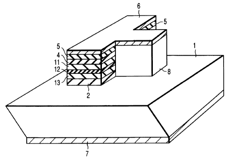
10 FIG. 1 is a perspective view showing a schematic
structure of a semiconductor light receiving element
according to a first embodiment of the present
invention.
FIG. 2 is a diagram showing a band-diagram at
15 the time of applying a reverse bias voltage to the
semiconductor light receiving element according to
the first embodiment of the present invention.
FIG. 3 is a diagram showing a band-diagram at the
time of applying a reverse bias voltage to a semicon-
ductor light receiving element according to a second
embodiment of the present invention.
FIG. 4 is a diagram showing a band-diagram at the
time of applying a reverse bias voltage to a semicon-
ductor light receiving element according to a third
embodiment of the present invention.
FIG. 5 is a diagram showing a band-diagram at
the time of applying a reverse bias voltage to
CA 02414293 2002-12-20
16
a semiconductor light receiving element according to
a fourth embodiment of the present invention.
FIG. 6 is a diagram showing a band-diagram at the
time of applying a reverse bias voltage to a semicon-
ductor light receiving element according to a fifth
embodiment of the present invention.
FIG. 7 is a perspective view showing a schematic
structure of a conventional semiconductor light
receiving element.
FIG. 8 is a cross-sectional view showing a
schematic structure of the conventional semiconductor
light receiving element.
FIG. 9 is a diagram showing a band-diagram at
the time of applying a reverse bias voltage to the
conventional semiconductor light receiving element.
Best Modes for Carrying Out of the Invention
Hereinafter, respective embodiments of the present
invention will be described with reference to the
figures.
(First Embodiment)
FIG. 1 is a perspective view showing a schematic
structure of a semiconductor light receiving element
according to a first embodiment of the present
invention.
In FIG. 1, portions which are the same as those of
the conventional semiconductor light receiving element
shown in FIG. 7 are denoted by the same reference
CA 02414293 2002-12-20
17
numerals, and details o~ duplicate portions will be
omitted.
Namely, as shown in FIG. l, a running layer 2
formed from non-doped type i-InP or n-type n-InP is
formed on the substrate 1 formed from n+-InP and
serving as an n-type semiconductor doped layer.
A second light absorbing layer 13 formed from
p-InGaAs, a spacer layer 12 formed from, for example,
non-doped type i-InGaAs, a first light absorbing layer
11 formed from p-InGaAs, a block layer 4, formed from
p+-InGaAsP and serving as a p-type semiconductor doped
layer, and a contact layer 5 formed from p+-InGaAs are
formed on the running layer 2.
The p electrode 6 is mounted on the top surface of
1S the contact layer 5.
An n electrode 7 is mounted on the bottom surface
of the above-described substrate 1.
Moreover, a polyimide 8 is formed in order to
reduce the capacitance, at a portion of the side
surfaces of the running layer 2, the second light
absorbing layer 13, the spacer layer 12, the first
light absorbing layer 11, the block layer 4, and the
contact layer 5, and at the bottom surface of the
p electrode 6.
Namely, the points that differ the most from the
conventional semiconductor light receiving element
shown in FIG. 7 are that the semiconductor light
CA 02414293 2002-12-20
18
receiving element of the first embodiment uses the
plurality of light absorbing layers 11, 13 formed from
the same semiconductor material of p-InGaAs, and the
spacer layer 12 formed from, for example, non-doped
type i-InGaAs is interposed between the plurality of
light absorbing layers 11, 13.
Note that, in the semiconductor light receiving
element of the first embodiment, the number of the
light absorbing layers 11, 13 is two layers, but may be
three or more layers as long as the spacer layer 12 is
sandwiched therebetween.
Note that it is known that an i-type (non-doped
type) semiconductor such as, for example, i-InGaAs or
the like, which forms the spacer layer 12, generally
has a slight n-type characteristic.
Accordingly, the spacer layer 12 is not limited
to an i-type (non-doped type) semiconductor such as
i-InGaAs or the like, and may be a layer formed from
a semiconductor material which allows electrons and
positive holes to accelerate and run.
For example, the above-described spacer layer 12
may be a layer formed from a semiconductor material
which is doped to n-type, or may be a layer formed from
a semiconductor material which is weakly (for example,
2S 1 x 101 cm-3) doped to p-type to an extent that
an internal electric field exists.
The semiconductor material of the spacer layer 12
CA 02414293 2002-12-20
19
may use a multi-quantum well structure in which
semiconductor materials are combined.
Further, the spacer layer 12 itself may be made
to function as a light absorbing layer for absorbing
light.
Here, a reverse bias voltage of a predetermined
value is applied between the p electrode 6 and the n
electrode 7.
FIG. 2 is a diagram showing a band-diagram of the
semiconductor light receiving element at the time of
applying the reverse bias voltage.
Next, features of the semiconductor light
receiving element according to the first embodiment of
the present invention, which is structured as described
above, will be described by using the band-diagram
shown in FIG. 2.
As described above, in the conventional
semiconductor light receiving element shown in FIG. 7
through FIG. 9, there is the problem that, if the
thickness of the light absorbing layer 3 is made
thicker than the diffusion length of the electrons in
order to highly-efficiently convert the incident light
into electrons 9 and positive holes 10, the electrons 9
generated as a result of the light being absorbed into
the light absorbing layer 3 cannot reach the running
layer 2, and high-speed operation is impossible.
On the other hand, in the semiconductor light
CA 02414293 2002-12-20
receiving element of the first embodiment according to
the present invention, because an electric field is
applied to the spacer layer 12 interposed between the
first and second light absorbing layers 11, 13, the
5 electrons 9 and the positive holes 10 generated by the
incident light being absorbed at the light absorbing
layers are accelerated at the spacer layer 12.
Accordingly, also when the light absorbing layer
is thicker than the diffusion length of the electrons
10 9, the light absorbing layer is divided into plural
layers formed from the first and second light absorbing
layers 11, 13, and the electrons 9 are accelerated at
the spacer layer 12 interposed between the two, and
thus, the electrons 9 can reach the running layer 2.
15 Further, in the semiconductor light receiving
element of the first embodiment according to the
present invention, the thickness of each light
absorbing layer doped to p-type is thin and is about
1/2 that of the prior art. Therefore, even if the
20 incident light amount of the light is small, the
electrons 9 can respond sufficiently quickly in the
respective light absorbing layers.
That is, in this case, even when the electrons 9
must move purely by only diffusion because the number
of electrons generated in the light absorbing layer
is few and repulsion thereamong cannot be expected,
since the thickness of each light absorbing layer
CA 02414293 2002-12-20
21
doped to p-type is thin, the electrons 9 can respond
sufficiently quickly.
On the other hand, because the thickness t of the
light absorbing layer is a total thickness (t1 + t2) of
respective thicknesses t1, t2 of the plurality of light
absorbing layers 11, 13, the efficiency of converting
the incident light into the electrons 9 and the
positive holes 10 can be markedly increased.
Accordingly, in accordance with the first
embodiment of the present invention, a high=speed and
highly efficient semiconductor light receiving element
can be realized.
Note that, as in the present embodiment described
above, when light is also absorbed at the spacer layer
12, the thickness thereof is added to the thickness
t of the light absorbing layer.
Moreover, although both of the electrons 9 and
the positive holes 10 run at the spacer layer 12, the
'thickness of the spacer layer 12 is thin and is about
0.3 ~tm or less, and thereby it suffices that a value of
the reverse bias voltage to be applied is small.
Next, the effect that the spacer layer 12 inserted
between the plurality of light absorbing layers has
on the capacitance of a semiconductor light receiving
element will be verified.
When the spacer layer 12 is one layer, considera-
tion of the capacitance can be simplified. Therefore,
CA 02414293 2002-12-20
22
consideration of the effects that the spacer layer 12
has on the capacitance of the entire semiconductor
light receiving element will be carried out by using
the semiconductor light receiving element of the first
embodiment shown in FIG. 1 and FIG. 2.
It is assumed that the capacitance caused at the
spacer layer 12 is CS, and the capacitance of the
running layer 2 is CM.
Thus, the capacitance CG of the entire
semiconductor light receiving element can be determined
by the equation (1) by synthesizing these two
capacitances CS and CM.
1/CG = (1/Cg) + (1/CM) ... (1)
Here, for example, when the thickness of the
spacer layer 12 is from several nm to several tens of
nm, the capacitance CS thereof is sufficiently large as
compared with the capacitance CM of the running layer 2
( for example, about 0 . 4 ~,m) .
Accordingly, in the equation (1), the first term
at the right side can be ignored as compared with
the second term at the right side. As a result,
the capacitance CG of the entire semiconductor light
receiving element is substantially equal to the
capacitance CM caused at the running layer 2.
In accordance therewith, the effect that the
spacer layer 12 has on the capacitance CG as of the
entire semiconductor light receiving element can almost
CA 02414293 2002-12-20
23
be ignored.
Conversely, when the capacitance CS of the spacer
layer 12 is small and is about the same as the
capacitance CM of the running layer 2, the capacitance
CG of the entire semiconductor light receiving element
becomes about the half of the capacitance Cg of the
spacer layer 12.
In the above description, for simplification,
the effect on the capacitance CG of the entire
semiconductor light receiving element is considered
for the embodiment having only one layer of the spacer
layer 12.
However, the fact that the spacer layer 12 does
not make the capacitance CG of the entire semiconductor
light receiving element large and does not adversely
affect the high-speed response is realized also by
light receiving elements, in which a plurality of
spacer layers 12 and a plurality of light absorbing
layers exist.
(Second Embodiment)
FIG. 3 is a diagram showing a band-diagram of
a semiconductor portion, at the time of applying
a reverse bias voltage, of a semiconductor light
receiving element according to a second embodiment of
the present invention.
In FIG. 3, portions which are the same as the
band-diagram of the semiconductor light receiving
CA 02414293 2002-12-20
24
element of the first embodiment shown in FIG. 2 are
denoted by the same reference numerals.
Note that a perspective view showing the structure
of the entire semiconductor light receiving element
according to the second embodiment of the present
invention is substantially the same as that of the
semiconductor light receiving element of the first
embodiment shown in FIG. 1.
Accordingly, here, mainly, only portions which
are different than the semiconductor light receiving
element of the first embodiment will be described.
As shown in FIG. 3, in the semiconductor light
receiving element of the second embodiment, a semicon-
ductor material whose band-gap wavelength is longer
than that of a first light absorbing layer lla is used
as a second light absorbing layer 13a.
In other words, as shown in FIG. 3, a band-gap
energy e2 of the second light absorbing layer 13a is
set to be smaller than a band-gap energy e1 of the
first light absorbing layer lla (e2 < e1).
For example, when light having a wavelength of
1.55 dun is absorbed, a semiconductor material whose
band-gap wavelength is longer than that of the first
light absorbing layer lla may be used as the second
light absorbing layer 13a.
For example, if p-InGaAsP or p-InGaAlAs having
band-gap wavelengths of 1.58 N.m and 1.62 dun,
CA 02414293 2002-12-20
respectively, are used as the semiconductor materials
of the first light absorbing layer lla and the second
light absorbing layer 13a, the semiconductor light
receiving element of the present embodiment can be
5 realized.
Moreover, p-InGaAsP or p-InGaAlAs may be used as
the first light absorbing layer 11a, and p-InGaAs
having a longer band-gap wavelength may be used as the
second light absorbing layer 13a.
10 Needless to say, the band-gap wavelengths are not
limited to these values.
Further, when three or more light absorbing layers
are used, p-InGaAsP or p-InGaAlAs is used such that the
band-gap wavelengths of the respective light absorbing
15 layers become longer in stages from the p electrode 6
side toward the n electrode 7 side, and p-InGaAs may
be used as the layer which is closest to the n
electrode 7.
In this way, in the semiconductor light receiving
20 element of the second embodiment of the present
invention, because the drifting effect in the spacer
portion 12 is greater and the electrons 9 are
accelerated more, as compared with the semiconductor
light receiving element of the first embodiment
25 described above, an even higher speed response is
possible.
CA 02414293 2002-12-20
26
(Third Embodiment)
FIG. 4 is a diagram showing a band-diagram of
a semiconductor portion, at the time of applying
a reverse bias voltage, of a semiconductor light
receiving element according to a third embodiment of
the present invention.
In FIG. 4, portions which are the same as the
band-diagram of the semiconductor light receiving
element of the first embodiment shown in FIG. 2 are
denoted by the same reference numerals.
Note that a perspective view showing the structure
of the entire semiconductor light receiving element
according to the third embodiment of the present
invention is substantially the same as that of the
semiconductor light receiving element of the first
embodiment shown in FIG. 1.
Accordingly, here, mainly, only portions which
are different than the semiconductor light receiving
element of the first embodiment will be described.
In the semiconductor light receiving element of
the third embodiment, the band-gap wavelength of
a first light absorbing layer llb and the band-gap
wavelength of a second light absorbing layer 13b are
equal to one another (band-gap energies; e1 = e2).
However, the p-type dopant concentrations thereof are
made to be different.
For example, if the p-type dopant concentration of
CA 02414293 2002-12-20
27
the first light absorbing layer llb is 1 x 1018 cm-3,
the p-type dopant concentration of the second light
absorbing layer 13b is set to be smaller, such as 5 x
1017 cm-3, than the p-type dopant concentration of the
first light absorbing layer 11b.
It goes without saying that the p-type dopant
concentrations are not limited to these values.
In this way, because the p-type dopant concentra-
tion of the second light absorbing layer 13b at the
n electrode 7 side is set to be smaller than the p-type
dopant concentration of the first light absorbing layer
llb at the p electrode 6 side, the effect of improving
the drifting at the spacer layer 12 increases.
Therefore, in the semiconductor light receiving
element of the third embodiment of the present
invention, because the electrons 9 are accelerated
more in the light absorbing layer, compared with the
semiconductor light receiving element of the first
embodiment shown in FIG. 2, an even higher speed
response is possible.
Note that, when three or more light absorbing
layers are used, it suffices that the p-dopant
concentrations of the respective light absorbing layers
are made to be smaller in order from the p electrode 6
side toward the n electrode 7 side.
Needless to say, the band-gap wavelengths of the
plurality of light absorbing layers may be different.
CA 02414293 2002-12-20
28
(Fourth Embodiment)
FIG. 5 is a diagram showing a band-diagram of
a semiconductor portion, at the time of applying
a reverse bias voltage, of a semiconductor light
receiving element according to a fourth embodiment of
the present invention.
In FIG. 5, portions which are the same as the
band-diagram of the semiconductor light receiving
element of the first embodiment shown in FIG. 2 are
denoted by the same reference numerals.
Note that a perspective view showing the structure
of the entire semiconductor light receiving element
according to the fourth embodiment of the present
invention is substantially the same as that of the
semiconductor light receiving element of the first
embodiment shown in FIG. 1.
Accordingly, here, mainly, only portions which
are different than the semiconductor light receiving
element of the first embodiment will be described.
In the semiconductor light receiving element of
the fourth embodiment, the band-gap wavelength of
a first light absorbing layer llc and the band-gap
wavelength of a second light absorbing layer 13c are
respectively set so as to become gradually longer,
namely, in an inclining manner, from the p electrode 6
side toward the n electrode 7 side.
In other words, as shown in FIG. 5, the band-gap
CA 02414293 2002-12-20
29
energy e1 of the first light absorbing layer llc and
the band-gap energy e2 of the second light absorbing
layer 13c are respectively set in an inclining manner
so as to gradually become smaller from the p electrode
6 side toward the n electrode 7 side.
In this way, by inclining the band-gap wavelengths
(band-gap energies) in the respective light absorbing
layers 11c, 13c, the electrons 9 can be accelerated in
the respective light absorbing layers 11c, 13c, as
well.
Accordingly, in the semiconductor light receiving
element of the fourth embodiment of the present
invention, as compared with the semiconductor light
receiving element of the second embodiment shown in
FIG. 3, in which the band-gap wavelengths are constant
in the respective light absorbing layers 11a, 13a,
an even higher speed response is possible.
Moreover, in the semiconductor light receiving
element of the fourth embodiment of the present
invention as well, the p-type dopant concentrations may
be set to become smaller from the p electrode 6 side
toward the n electrode 7 side.
(Fifth Embodiment)
FIG. 6 is a diagram showing a band-diagram of
a semiconductor portion, at the time of applying a
reverse bias voltage of a semiconductor light receiving
element according to a fifth embodiment of the present
CA 02414293 2002-12-20
invention.
In FIG. 6, portions which are the same as the
band-diagram of the semiconductor light receiving
element of the first embodiment shown in FIG. 2 are
5 denoted by the same reference numerals.
Note that a perspective view showing the structure
of the entire semiconductor light receiving element
according to the fifth embodiment of the present
invention is substantially the same as that of the
10 semiconductor light receiving element of the first
embodiment shown in FIG. 1.
Accordingly, here, mainly, only portions which
are different than the semiconductor light receiving
element of the first embodiment will be described.
15 In the semiconductor light receiving element of
the fifth embodiment, in a first light absorbing layer
lld and a second light absorbing layer 13d, the p-type
dopant concentrations are set to be low to an extent
.that an internal electric field strength exists.
20 In this way, in the semiconductor light receiving
element of the fifth embodiment, because the electrons
9 and the positive holes 10 are accelerated in the
first light absorbing layer lld and the second light
absorbing layer 13d by setting the p-type dopant
25 concentrations in the respective light absorbing layers
11d, 13d to be low, an even higher speed response is
possible.
CA 02414293 2002-12-20
31
However, in this case, if the values of the p-type
dopant concentrations in the respective light absorbing
layers 11d, 13d are set to be too low, the electric
field strength for making the positive holes 10 move
becomes large.
As a result, the necessary bias application
voltage also becomes that much greater.
In accordance therewith, there is concern that
destruction of the semiconductor light receiving
element will arise due to Joule heat as described
above.
Accordingly, the p-type dopant concentrations in
the respective light absorbing layers 11d, 13d must be
set within a range in which this can be avoided.
The present invention is not limited to the
respective embodiments described above.
In the semiconductor light receiving elements of
the respective embodiments, the number of light
absorbing layers is two layers. However, the present
invention has the feature that the spacer layer for
acceleration is provided between the plurality of light
absorbing layers.
Accordingly, as long as this condition is
satisfied, it goes without saying that there may be
three or more light absorbing layers.
In the respective embodiments, the semiconductor
materials of the spacer layers 12 are not limited to
CA 02414293 2002-12-20
32
the same semiconductor materials as the respective
light absorbing layers 11, 13, and it is possible to
use other semiconductor materials including InP,
InAlAs, InGaAsP, InGaAlAs, and the like.
In addition, a multi-quantum well structure in
which semiconductor materials are combined may be used
as the semiconductor material of the spacer layer 12.
Meanwhile, the generated amount of noise of the
semiconductor light receiving element can be reduced by
setting the band-gap energy a of the spacer layer 12 to
be large.
As described above, the spacer layer 12 is not
limited to an i-type (non-doped type) semiconductor
such as i-InGaAs or the like, and may be a layer formed
from a semiconductor material which can make the
electrons and the positive holes accelerate and run in
the interior thereof.
For example, the above-described spacer layer 12
may be a layer formed from a semiconductor material
doped to n-type, or may be a layer formed from
a semiconductor material weakly doped to p-type to
the extent that an internal electric field exists.
Further, the spacer layer itself may be made to
function as a light absorbing layer absorbing light.
Moreover, when a notch can be formed in the band
at the junction between the light absorbing layer and
the spacer layer, if doping by p-type dopant having
CA 02414293 2002-12-20
33
a high concentration is carried out at the light
absorbing layer side and the dopant is inserted into
the junction, the notch of the band can be made small.
In the respective embodiments, it was assumed that
the wavelength of the incident light is 1.55 dun, but
the wavelength may be another wavelength such as 1.3 ~m
or the like.
Further, the semiconductor materials of the
light absorbing layers may be, instead of p-InGaAs,
and instead of a four-source mixed crystal such as
p-InGaAsP, p-InGaAlAs, or the like, a multi-quantum
well doped to p-type.
In addition, the semiconductor material of the
contact layer 5 can use, instead of p+-InGaAs, various
types of semiconductor materials such as p+-InGaAsP or
the like.
As described above, in accordance with the
semiconductor light receiving element of the present
invention, the light absorbing layer is formed from
plural layers, and the spacer layer for acceleration is
provided between the plural light absorbing layers.
Namely, the semiconductor light receiving element
of the present invention is used in which the spacer
layer for acceleration having a drifting effect is
sandwiched between the plurality of light absorbing
layers which are doped to p-type.
Therefore, in accordance with the present
CA 02414293 2002-12-20
34
invention, as compared with the case in which the
conventional light absorbing layer is one layer and is
thick, the diffusion state of the electrons determining
the response speed of the semiconductor light receiving
element is greatly improved. As a result, a high-speed
response as a semiconductor light receiving element is
possible.
Moreover, in the semiconductor light receiving
element in accordance with the present invention,
because the thickness of each light absorbing layer
doped to p-type is thin and is about 1/2 compared with
the prior art, even if the incident light amount of
light is small, the electrons can respond sufficiently
quickly in each light absorbing layer.
That is, in this case, also when the electrons
must move purely by only diffusion because the number
of electrons generated in the light absorbing layer is
small and the repulsion thereamong cannot be expected,
the thickness of each of the doped light absorbing
layers is thin, and thereby the electrons can respond
sufficiently quickly.
On the other hand, with regard to the incident
light, because the thickness of the light absorbing
layer is the total thickness of the respective
thicknesses of the plurality of light absorbing layers,
the efficiency of the incident light being converted
into the electrons and the positive holes can be
CA 02414293 2002-12-20
markedly increased.
Accordingly, compared with the conventional
UTC-PD, in the semiconductor light receiving element
of the present invention, a rapid frequency response
5 characteristic can be realized even when the incident
light amount of light is small.
In accordance therewith, in the semiconductor
light receiving element of the present invention, there
is no need to use a fiber amplifier before light is led
10 to the light receiving element, and it is advantageous
also from the standpoint of the cost of a communication
system.
As described above in detail, according to
the present invention, it is possible to provide
15 a semiconductor light receiving element in which, by
interposing a spacer layer for acceleration between
a plurality of light absorbing layers, high-speed
movement of electrons at the light absorbing layers is
possible, and which can use a light absorbing layer
20 which is thick on the whole, and which is high-speed
and highly efficient regardless of the magnitude of the
incident light amount, and to provide a method of
manufacturing the same.