Note: Descriptions are shown in the official language in which they were submitted.
CA 02414325 2002-12-13
METHOD OF FABRICATING GaN SEMICONDUCTOR STRUCTURES
USING LASER-ASSISTED EPITAXIAL LIFTOFF
BACKGROUND OF THE INVENTION
The present invention relates generally to nitride based semiconductor
structures, and
s more particularly to a method of fabricating a nitride based .resonant
cavity semiconductor
structure by laser-assisted epitaxial lift-off to move the semiconductor
structure from a first
substrate to a second substrate to allow fabrication of distributf;d Bragg
reflectors (DBRs) on
both sides of the nitride based resonant cavity semiconductor structure.
A planar mufti-layered semiconductor structure can have one or more active
to semiconductor layers bounded at opposite sides with semiconductor layers
that form distributed
Bragg reflectors. The distributed Bragg reflectors at opposite sides of the
active semiconductor
layer are formed from alternating high refractive index and low refractive
index quarter-
wavelength thick semiconductor or dielectric layers that function as mirrors.
The multiple
semiconductor layers including the active semiconductor layer, between the
opposing distributed
15 Bragg reflectors, form a resonant cavity for Iight emission or light
absorption within the
semiconductor structure. The active semiconductor layers within the resonant
cavity will either
emit light for a light emitting diode (LED) or vertical cavity surface
emitting laser (VCSEL) or
absorb light for a photodetector (PD).
The semiconductor layers on one side of the acfiive layer in the structure are
doped with
20 impurities so as to have an excess of mobile electrons. These layers with
excess electrons are
said to be n-type, i.e. negative. The semiconductor layers on the other side
of the active layer in
the structure are doped with impurities so as to have a deficiency of mobile
electrons, therefore
creating an excess of positively charged carriers called holes. These layers
with excess holes are
said to be p-type, i.e. positive.
25 A forward biased electrical potential is applied through electrodes between
the p-side and
the n-side of the layered structure, thereby driving either holes or electrons
or both in a direction
perpendicular to the planar layers across the p-n junction so as to "inject"
them into the active
layers, where electrons recombine with holes to produce light. A, light
emitting diode will emit
light from the resonant cavity through one of the DBRs through the upper or
lower surface of the
t
CA 02414325 2002-12-13
semiconductor structure. For a laser, optical feedback provided by the
opposing DBRs allows
resonance of some of the emitted light within the resonant cavity to produce
amplified stimulated
emission of coherent "lasing" through one of the DBRs through either the upper
surface or the
lower surface of the semiconductor laser structure.
For a photodetector, a reverse biased electrical potential is applied through
the electrodes
between the p-side and the n-side of the layered structure. A photodetector
will absorb light in
the active layer of the resonant cavity, thereby driving electron/hole pairs
from the active layer to
be collected to form a photocurrent.
Nitride based semiconductors, also known as group III nitride semiconductors
or Group
to III-V semiconductors, comprise elements selected from group III, such as
Al, Ga and In, and the
group V element N of the periodic table. The nitride based semiconductors can
be binary
compounds such as gallium nitride (GaN), as well as ternary alloys of aluminum
gallium nitride
(AIGaN) or indium aluminum nitride (InGaN), and quarternary alloys such as
aluminum gallium
indium nitride (AIGaInN). These materials are deposited on substrates to
produce layered
semiconductor structures usable as light emitters for optoelectronic device
applications. Nitride
based semiconductors have the wide bandgap necessary for short-wavelength
visible light
emission in the green to blue to violet to the ultraviolet spectrum.
These materials are particularly suited for use in short-wavelength VCSELs or
LEDs for
several important reasons. Specifically, the InGaAIN system has a large
bandgap covering the
2o entire visible spectrum. III-V nitrides also provide the important
advantage of having a strong
chemical bond which makes these materials highly stable and resistant to
degradation under the
high electric current and the intense light illumination conditions that are
present at active
regions of the devices. These materials are also resistant to dislocation
formation once grown.
Semiconductor resonant cavity structures comprising nitride semiconductor
layers grown
on a sapphire substrate will emit or absorb light in the near ultra-violet to
visible spectrum within
a range including 280 nm to 650 nm, allowing better efficiency and narrower
line widths for
LEDs and photodetector.
The shorter wavelength blue of nitride based semiconductor VCSELs and LEDs
provides
a smaller spot size and a better depth of focus than the longer wavelength of
red and infrared (IR)
3o VCSELs and LEDs for high-resolution or high-speed laser printing operations
and high density
2
CA 02414325 2002-12-13
optical storage. In addition, blue light emitting devices can potentially be
combined with existing
red and green lasers or LEDs to create projection displays and color film
printers.
In many applications, the conventional substrate material for semiconductor
structures
would be silicon or gallium arsenide. However, the GaN crystal structure,
combined with the
high GaN growth temperatures, make deposition of high-quality nitride
semiconductor material
directly onto semiconductor substrates such as Si or GaAs very difficult.
Nitride based semiconductor structures currently require heteroepitaxial
growth of GaN
thin layers onto dissimilar substrates such as sapphire or silicon carbide.
The most commonly used growth substrate, sapphire, still imposes constraints
on the
1o GaN layer quality due to the lattice and thermal-expansion coefficient
mismatch between the
GaN and the sapphire. The disparate properties of these two materials result
in a high density of
extended defects, such as dislocations and stacking faults, at the GaN thin
layer/sapphire
substrate interface.
Many substrate separation techniques are available including wet-chemical
etching,
chemical-mechanical polishing or laser-assisted lift-off. Wet-chemical etching
and chemical-
mechanical polishing are inherently slow processes that require high
selectivity in materials in
order to remove the original growth substrate. Laser assisted lift-off
processes have several
advantages over the chemically assisted methods for the GaN thin film/sapphire
substrate
system. The laser processing is optically selective, possesses spatial control
and is a relatively
2o fast lift-off technique.
In order for the substrate separation technique to be successfully
implemented, the
technique itself must not degrade the quality of the GaN layer being
processed. The laser process
introduces a thermoelastic stress to the GaN layer, due to the rapid heating
and cooling during
the pulsed irradiation, that may fracture the GaN layer. Thin film fracture
may arise from
2s microcracks within the biaxially stressed GaN or from a thermal shock
initiating microcrack
propagation through the GaN layer.
An inherent problem when depositing thick GaN layers heteroepitixally onto
sapphire or
Gags is the intrinsic stress, compressive for sapphire and tensile for GaAs,
regardless of the
substrate separation technique, due to the thermal coefficient mismatch
between the GaN film
3o and the substrates.
3
' CA 02414325 2002-12-13
The success of the growth substrate removal to create a CraN substrate is
dictated, in part,
by the quality of the as-grown GaN layer. Due to complications related to
heteroepitaxy, thick
GaN layers; like those needed for a substrate, generally possess microcracks
that can propagate
and multiply during the laser lift-off process. The combination of the
intrinsic residual stress and
the thermoelastic stress of the laser processing gives rise to crack
propagation across the entire
GaN wafer area. The crack propagation would lead to uncontrolled catastrophic
mechanical
failure of the GaN or, at least, ill-defined low-quality GaN substrates.
Another problem specific to fabricating GaN VCSELs is the difficulty in
growing the
highly reflective AIGaN-based distributed Bragg reflectors (DBRs) needed for
stimulated
1o emission of coherent light of VCSELs, where the minimum aluminum content
for the AIGaN
layers in the DBRs is limited by self absorption of the light and the maximum
aluminum content
is limited by lattice matching constraints.
Similar problems plague the long wavelength indium phosphide VCSELs but the
problem in phosphide based laser structures can be solved by etching a hole
through the substrate
and evaporating dielectric materials to form the DBR. Unfortunately, the usual
substrate for
nitride based structures, i.e. sapphire, is difficult to dry or wet etch, so
that this back-etch
procedure is not available to the fabrication of the nitride based laser
structure.
It is an object of the present invention to provide distributed Bragg
reflectors (DBRs) on
both sides of the nitride based resonant cavity semiconductor structure.
SUMMARY OF THE INVENTION
According to the present invention, a nitride based resonant cavity
semiconductor
structure with a first distributed Bragg reflector is fabricated on a sapphire
substrate, a second
substrate is bonded to the first distributed Bragg reflector, the sapphire
substrate is removed by
laser-assisted epitaxial lift-off, and a second Bragg reflector is fabricated
on the VCSEL structure
opposite the first distributed Bragg reflector. The nitride based resonant
cavity semiconductor
structure can be a VCSEL, LED or photodetector, or a combination of said
devices.
Other objects and attainments together with a fuller understanding of the
invention will
become apparent and appreciated by referring to the following description and
claims taken in
3o conjunction with the accompanying drawings.
4
CA 02414325 2002-12-13
BRIEF DESCRIPTION OF THE DRAWINGS
A more complete appreciation of the invention and many of the attendant
advantages
thereof will be readily obtained and understood by referring to the following
detailed description
and the accompanying drawings in which like reference numerals denote like
elements as
between the various drawings. The drawings, briefly described below, are not
to scale.
Figure 1 is a side view of a nitride based resonant cavity semiconductor
structure with a
first distributed Bragg reflector on a sapphire substrate in accordance with a
first embodiment of
the present invention.
1o Figure 2 is a side view of the laser lift-off process for removing the
sapphire substrate
from the nitride based resonant cavity semiconductor structure with a first
distributed Bragg
reflector of Figure 1.
Figure 3 is a side view of the inverted nitride based resonant cavity
semiconductor
structure of Figure 1 with a second distributed Bragg reflector.
DETAILED DESCRIPTION
In the following detailed description, numeric ranges are provided for various
aspects of
the embodiments described. These recited ranges are to be treated as examples
only, and are not
intended to limit the scope of the claims hereof. In addition, a number of
materials are identified
2o as suitable for various facets of the embodiments. These recited materials
are to be treated as
exemplary, and are not intended to limit the scope of the claims hereof. In
addition, the figures
are not drawn to scale for ease of understanding the present invention.
Reference is now made to the Figures, wherein there is illustrated a nitride
based resonant
cavity semiconductor structure with distributed Bragg reflectors (DBRs) on
opposite sides of the
active layer in accordance with this invention. The nitride based resonant
cavity semiconductor
structure can be vertical cavity surface emitting laser (VCSEL), a light
emitting diode (LED), or
a photodetector (PD), or a combination of these devices. Gallium nitride
semiconductor layers
are grown on a sapphire substrate by techniques such as organometallic vapor
phase epitaxy
("OMVPE") or hydride vapor phase epitaxy ("HYPE") as is well-known in the art.
s
CA 02414325 2002-12-13
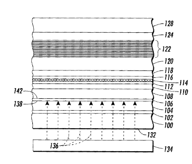
In Figure l, OMVPE growth is typically performed on a sapphire substrate 100.
The
substrate 100 can be a C-face (0001) or A-face (112_0) oriented sapphire
(A1203) substrate. The
sapphire substrate 100 is of standard specifications including an epitaxial
polish on one or both
sides and a typical thickness ranging on the order of 200 ~,m to 1000 p,m.
A gallium nitride nucleation layer 102 is first grown on the sapphire
substrate 100. A
gallium nitride layer 104 is then grown on the nucleation layer 102.
The substrate temperatures during growth are typically 550 degrees C for the
approximately 200 Angstrom thin GaN nucleation layer 102 and 1000 degrees C to
1200 degrees
C for the GaN layer 104. The deposition rates are typically in the order of 1
pm/hour to 20
~mlhour. The thick GaN layer 104 has typically a depth ranging between 60 ~.m
to 300 ~.m. In
addition, the reactor pressure may be controlled between 50 Torr and 1500
Torr. As
organometallic precursors, TMGa (trimethylgallium) or TEGa (triethylgallium)
can be used for
the group III elements and NH3 (ammonia) can be used as the nitrogen source.
Hydrogen and/or
nitrogen are used as carrier gas for the metalorganic sources.
Another deposition technique for the growth of a thick GaN layer well known in
the art is
HVPE. HVPE growth is also typically performed on a sapphire substrate. The
substrate 100 can
be a C-face (0001) or A-face (112_0) oriented sapphire (A12U3) substrate.
However, other
substrate orientations may also be used. The substrate temperatures during
growth are typically
500 to 600 degrees C for the thin GaN nucleation layer 102 and 1000 degrees C
to 1200 degrees
2o C for the thick GaN layer 104. The deposition rates are typically in the
order of 10 p,m/hour up to
several 100 pm/hour. GaCI is used as group III element source, which is
produced by flowing
HCl gas over liquid gallium. NH3 (ammonia) is used as the nitrogen source.
Hydrogen and/or
nitrogen are used as carrier gases.
In principle, other deposition methods like molecular beam epitaxy ("MBE")
could be
used, although the relatively small deposition rates of MBE would make it
difficult to grow thick
GaN layers. One can also use a combination of the above mentioned deposition
techniques. For
example OMVPE could be used to grow a high quality GaN nucleation layer 102
with a depth of
approximately 1-2 p.m and HYPE can be used subsequently to grow the very thick
GaN layer
104 on top of the nucleation layer 102.
6
CA 02414325 2002-12-13
A laser absorption InGaN layer 106 is then grown on the GaN buffer layer 104.
The
sacrificial layer 106 typically has a thickness of between 1500 angstroms and
4000 angstroms.
A III-V nitride contact layer 108 is formed on the laser absorption layer 106.
The III-V
nitride layer 108 is an n-type GaN:Si layer acting as a lateral n-contact and
current spreading
layer. The contact and current spreading layer 108 typically has a thickness
of from about 1 ~,m
to about 20 gum.
A III-V nitride cladding layer 110 is formed over the contact layer 108. The
III-V nitride
layer 110 is an n-type AIGaN:Si cladding layer. The cladding layer 110
typically has a thickness
of from about 0.2 hum to about 2 ~,m.
to On top of the III-V nitride cladding layer 110, a III-V nitride waveguide
layer 112 is
formed followed by the III-V nitride quantum well active region 114. The n-
type GaN:Si
waveguide layer 112 typically has a thickness of from about 50 nm to about 200
nm. The
quantum well active region 114 is comprised of at least one InGaN quantum
well. For multiple-
quantum well active regions, the individual quantum wells typically have a
thickness of from
about 10 ~ to about 100 ~ and are separated by InGaN or GaN barrier layers
which have
typically a thickness of from about 10 ~ to about 200 t~..
A III-V nitride waveguide layer 116 is formed over the quantum well active
region 114.
The p-type GaN:Mg layer 116 serves as a waveguide layer and ha,s a thickness
of from about 50
nm to about 200 nm.
2o A III-V nitride cladding layer 118 is formed over the waveguide layer 116.
The p-type
AIGaN:Mg layer 118 serves as a cladding and current confinement layer. The III-
V nitride
cladding layer 118 typically has a thickness of from about 0.2 ~,m to about 1
~,m.
A III-V nitride contact layer 120 is formed over the cladding layer 118. The p-
type
GaN:Mg layer 120 forms a p-contact layer for the minimum-resistance metal
electrode to contact
the p-side of the laser heterostructure 100. The III-V nitride contact layer
120 typically has a
thickness of from about 10 nm to 200 nm.
A first distributed Bragg reflector 122 is formed over the p-contact layer
120. The first
distributed Bragg reflector 122 has six pairs of quarter-wavelength thick
alternating silicon
dioxide (Si02) and tantalum pentoxide (Ta205) dielectric layers. Alternately,
the DBR can have
3o alternating layers of SiOZ/Ti02 or GaN/AIGaN or alternating layers of AIGaN
with different
7
CA 02414325 2002-12-13
aluminum content. Also, the DBR can have more or less than six pairs of
alternating layers, if
higher reflectivity is desired. However, fewer number of pairs may be desired
in the case of
photodetectors in order to enhance light extraction.
A gold Au layer 124 is formed over the first distributed Bragg reflector 122.
The gold
overlayer 124 has a typical thickness of 20 to 200 nm.
The upper surface 126 of the gold overlayer 124 is bonded to a silicon (Si)
substrate 128
using an adhesive bond 130. The adhesive 124 may be a cyanoacrylate-based
glue. The support
substrate could alternatively be gallium arsenide (GaAs), copper or any rigid
material. The
adhesive could alternately be a thin film adhesive, spin-on glass, or any
appropriate solder. The
1 o use of copper or other metals as the support substrate 128 bonded to the
gold layer 124 provides
good thermal conductivity.
The lower surface 132 of the sapphire substrate 100 is polished to a very
smooth surface
finish to minimize light scattering. Polishing is accomplished mechanically
using a succession
of diamond pads (not shown). During the polishing procedure, the diamond grit
size is gradually
i5 reduced from a grit size of about 30 p,m down to a grit size of 0.1 ~,m.
Typical root mean square
(rms) roughness after polishing is about 20-50 Angstrom. Polishing may be done
before bonding
to the support substrate.
As shown in Figure 2, an ultraviolet excimer laser 134 then emits a laser beam
136 which
is transmitted through the sapphire substrate 100 to the interface 138 between
the GaN buffer
20 layer 104 and the laser absorption InGaN layer 106. Sapphire and gallium
nitride are transparent
to the wavelength of the light beam emitted by the laser. Proper adjustment of
the excimer laser
allows decomposition of the thin laser absorption InGaN layer 106 at the
interface 138 between
the GaN buffer layer 104 and the sacrificial InGaN layer 106.
The InGaN layer 106 is decomposed into indium and gallium metal and gaseous
nitrogen
25 by the radiation from the laser beam through the sapphire substrate and the
gallium nitride layer.
The InGaN layer 106 is a laser absorption layer with the wavelength of the
light beam 136
matching the decomposition of the indium.
A homogenizer (not shown) converts the Gaussian-profile beam emitted by the
laser to a
flat plateau-like laser beam which provides improved beam uniformity.
8
' CA 02414325 2002-12-13
A larger surface area of the laser absorption InGaN layer may be exposed by
scanning the
laser beam across the interface surface rather than providing a stationary
beam. The excimer
laser is typically pulsed in the range of 5-10 Hz with one pulse typically
being sufficient to
achieve decomposition of the GaN layer. The polished lower surface 132 of the
sapphire
substrate 100 allows uniform excimer laser exposure of the InGaN layer 106.
After separation of the sapphire substrate 100 and the gallium nitride layers
102 and 104
from the nitride based resonant cavity semiconductor structure 140, any
residual indium or
gallium metal on the surface 142 of the GaN contact layer 108 is removed with
a hydrochloric
acid (HCL) and water solution dip (HCL:H20 = l :l).
1o The sapphire substrate 100 is reusable for subsequent fabrication of
nitride based
semiconductor structures. The substrate 100 need not be sapphire but can be
any optically
transparent material which is transmissive to the wavelength of the light beam
136 from the laser
134 and suitable for growth of GaN layers on its surface.
As shown in Figure 3, the semiconductor structure 140 is then inverted with
the silicon
(Si) substrate 128 and the p-doped layers down and the n-contact layer 108 on
top of the inverted
laser structure.
Dry-etching using CAIBE (chemical assisted ion beam etching) or RIE (reactive
ion
beam etching) in an Ar/Cl2BCl3 gas mixture is used to etch the semiconductor
structure 140
through the n-contact layer 108, the n-cladding layer 110, the n-waveguide
layer 112, the InGaN
2o active region 114, the p-waveguide layer 116, the p-cladding layer 118 down
to expose the
GaN:Mg current-spreading and p-contact layer 120.
A second distributed Bragg reflector 142 is formed over the central portion of
the n-
contact layer 108. The second distributed Bragg reflector 142 has six pairs of
quarter-
wavelength thick alternating silicon dioxide (Si02) and tantalum pentoxide
(Ta205) dielectric
layers. Alternately, the DBR can have alternating layers of Si02/Ti02 or
GaN/AIGaN or
alternating layers of AIGaN with different aluminum content. Also, the DBR can
have more or
less than six pairs of alternating layers, depending upon the specific device.
A p-type Ni/Au electrode 144 is formed an the etched, exposed p-current-
spreading layer
120 of the semiconductor structure 140, which is functioning as a lateral
contact layer.
9
CA 02414325 2002-12-13
An n-type Ti/Al electrode 146 is formed on the exposed n-contact layer 118 of
the
semiconductor structure 140, surrounding the second DBR 142.
The resonant cavity 148 of the semiconductor structure 140 between the first
DBR 122
and the second DBR 142 consists of the n-contact layer 108, the n-cladding
layer 110, the n-
waveguide layer 112, the InGaN active region 114, the p-waveguide layer 116,
the p-cladding
layer 118, and the p-contact layer 120.
The nitride based resonant cavity semiconductor structura 140 can be either a
vertical
cavity surface emitting laser (VCSEL), a light emitting diode (LED, or a
photodetector (PD), or a
combination of these devices.
to If the semiconductor structure 140 is a VCSEL, then the first DBR 122 and
the second
DBR 142 are highly reflective by increasing the number of high refractive
index/low refractive
index semiconductor or dielectric layer pairs and/or increasing the difference
between the high
refractive index and low refractive index. A forward biased electrical
potential is applied
between the p-electrode 144 and the n-electrode 146 causing emission of light
from the active
region 114 which is amplified in the resonant cavity 148 by continuous
reflection between the
two DBRs 122 and 142 before emission of coherent light 1 SO through the second
DBR 142 of
the VCSEL structure 140.
If the semiconductor structure 140 is a LED, then the second DBR 142 is less
reflective
than those of a VCSEL by decreasing number of high refractive index/low
refractive index
2o dielectric or semiconductor layer pairs and/or decreasing the difference
between the high
refractive index and low refractive index. A forward biased electrical
potential is applied between
the p-electrode 144 and the n-electrode 146 causing emission of light 150 from
the active region
114 in the resonant cavity 148 through the second DBR 142 of the LED structure
140.
If the semiconductor structure 140 is a photodetector, then the second DBR 142
is less
reflective than those of a VCSEL by decreasing number of high refractive
index/low refractive
index dielectric or semiconductor layer pairs and/or decreasing the difference
between the high
refractive index and low refractive index.
A reverse biased electrical potential is applied between the p-electrode 144
and the n-
electrode 146 causing absorption of light 150 in the active region 114 in the
resonant cavity 148
to
CA 02414325 2002-12-13
through the second DBR 142 of the LED structure 140. T he absorption will
produce a
photocurrent.
Alternately, the nitride based resonant cavity semiconductor structure can be
fabricated
with the p-doped semiconductor layers up by removing the epitaxial layer host
layer after
forming the second DBR, then transfer to a support substrate. The laser
assisted epitaxial lift-off
of the sapphire substrate and then the inversion of the semiconductor
structure will form the
more traditional n-side down, p-side up semiconductor structure.
Alternatively, a gold thin layer
can be deposited on the second DBR and a thick metal, such as copper, can be
plated to form the
support substrate.
1o The nitride based resonant cavity semiconductor structure can emit light
from the VCSEL
or LED or absorb light from the photodetector if the substrate is transparent
to the wavelength of
light emitted or absorbed and the lower DBR has less reflectivity than the
upper DBR.
The use of laser-assisted epitaxial lift-off of the first sapphire substrate
allows access to
the backside of nitride based semiconductor layers for the fabrication of
distributed Bragg
1 s reflectors on both sides of the nitride based resonant cavity
semiconductor structure.
An integrated nitride based resonant cavity semiconductor structures can be
fabricated
with a VCSEL and a photodetector, or a LED and a photodetector, or a VCSEL and
a LED, or
with a VCSEL, LED and a photodetector.
While the invention has been described in conjunction witlh specific
embodiments, it is
2o evident to those skilled in the art that many alternatives, modifications,
and variations will be
apparent in light of the foregoing description. Accordingly, the invention is
intended to embrace
all other such alternatives, modifications, and variations that fall within
the spirit and scope of
the appended claims.
11