Note: Descriptions are shown in the official language in which they were submitted.
CA 02414458 2010-04-01
TITLE OF THE INVENTION
Optical Transmission Systems including Optical Amplifiers
and Methods of use therein
BACKGROUND OF THE INVENTION
The present invention is directed generally to optical
systems. More particularly, the invention is directed toward
optical transmission systems including amplifying devices,
such as optical amplifiers.
The continued growth in traditional communications
systems and the emergence of the Internet as a means for
accessing data has accelerated demand for high capacity
communications networks. Telecommunications service
providers, in particular, have looked to wavelength division
multiplexing (WDM) to increase the capacity of transmission
systems to meet the increasing capacity demands placed on
their network infrastructure.
In WDM transmission systems, pluralities of distinct
information signals are carried using electromagnetic waves
having different wavelengths in the optical spectrum,
typically using infrared wavelengths. Each information
carrying wavelength can include multiple data streams that
are time division multiplexed ("TDM") together into a TDM
data stream or a single data stream.
The pluralities of information carrying wavelengths are
combined into a "WDM" optical signal that is transmitted in
a single waveguide. In this manner, WDM systems can increase
the transmission capacity of the network compared to space
division multiplexed ("SDM"), i.e., single channel, systems
by a factor equal to the number of wavelengths used in the
WDM system.
Optical WDM systems were not initially deployed, in
part, because of the high cost of electrical signal
regeneration/amplification equipment required to
compensate for signal attenuation for each optical
-1-
CA 02414458 2003-01-06
WO 02/05462 PCT/US01/21471
wavelength throughout the system. However, the
development of the erbium doped fiber amplifier (EDFA)
provided a cost effective means to amplify optically
multiple optical signal wavelengths in the 1550 nm range.
In addition, the 1550 nm signal wavelength range
coincides with a low loss transmission window in silica
based optical fibers, which allowed EDFAs to be spaced
further apart than conventional electrical
repeaters/regenerators.
Optical amplifiers are deployed periodically, e.g.,
40-120 km, throughout the optical system to compensate
for attenuation that incurs in a span of optical fiber
preceding the amplifier. The amplifiers are operated so
that the gain provided by the optical amplifier
compensates, or substantially compensates, for the loss
in each span. As a result, no net loss or gain of signal
power occurs in each span, i.e. Amplifier Gain = Span
Loss, which is referred to as transparent operation.
The use of EDFAs essentially eliminated the need
for, and the associated costs of, electrical signal
repeater/regeneration equipment to compensate for signal
attenuation in many systems. The dramatic reduction in
the number of electrical regenerators in the systems,
made the installation of WDM systems in the remaining
electrical regenerators a cost effective means to
increase optical network capacity.
WDM systems have quickly expanded to fill the
limited amplifier bandwidth of EDFAs. New erbium-based
fiber amplifiers (L-band) have been developed to expand
the bandwidth of erbium-based optical amplifiers. Also,
new transmission fiber designs are being developed to
provide for lower loss transmission in the 1400-1500 nm
and 1600-1700 nm ranges to provide additional capacity
for future systems.
In addition, Raman fiber amplifiers ("RFA") have
been investigated for years and are now being
commercially deployed and operated in a network. RFAs
- 2 -
CA 02414458 2010-04-01
offer the potential to exploit a substantial portion of the
optical waveguide transmission capacity.
While optical amplifiers have provided significant
benefits by eliminating the need for numerous electrical
regenerators, optical amplifiers do have a shortcomings. For
example, optical amplifiers often do not provide uniform
amplification, or gain, profile over the signal wavelength
range. As such, optical amplifiers often will be deployed in
combination with gain flattening filters, which provide
wavelength specific filtering to produce a more uniform
gain.
In addition, the gain profile of the optical amplifier
can vary depending upon the amount of gain being provided by
the amplifier. In operating system, the amplifier gain is
set to compensate signal power attenuation that occurs in a
fiber span preceding the amplifier. The attenuation in each
span, i.e., the span loss, generally varies from span to
span in a system; therefore, the optical amplifiers have to
be operated at different gains corresponding to the span
loss. However, operation at different gain can introduce
gain profile variations that result in signal power
variations, which can degrade system performance.
While it is possible to design gain flattening filters
and amplifiers for specific span losses, individualized
amplifier and filter designs generally are not feasible from
a commercial standpoint. As such, amplifiers generally are
designed for a nominal gain and gain flattening filters are
designed based on that nominal gain. When the amplifiers and
filters are deployed in the system, operation of the
amplifiers at gains other than the nominal gain will
introduce signal power variations into the system.
Alternative designs have been proposed, in which the
amplifiers are operated at the designed nominal gain and a
variable attenuator is provided proximate the amplifier to
introduce additional attenuation into the span. The
variable attenuator is controlled, such that the variable
-3-
CA 02414458 2003-01-06
WO 02/05462 PCT/US01/21471
attenuator loss plus the span loss is equal to the
nominal gain of the amplifier.
The variable attenuator configurations allow the
operation of optical amplifiers at designed gains
allowing for more uniform gain profiles. However, the
introduction of excess gain balanced by excess
attenuation introduces additional noise into the system
that also degrades system performance. In addition,
these alternative designs require that the amplifier be
designed to provide high gain that can be attenuated to
accommodate various span loss, which can increase overall
amplifier and system costs.
The development of higher performance, lower cost
communication systems depends upon the continued
development of higher performance components and
subsystems for use in the system. It is, therefore,
essential that optical systems and optical amplifiers be
developed having increased performance capabilities to
meet the requirements of next generation optical systems.
BRIEF SUMMARY OF THE INVENTION
The apparatuses and methods of the present invention
address the above need for improved optical transmission
systems and optical amplifiers. Optical transmission
systems of the present invention include a plurality of
optical amplifiers configured to provide sufficient
cumulative signal amplification, or gain, to compensate
for cumulative signal attenuation, or loss, in the
system. The gain of each individual amplifier is not
adjusted to compensate for the loss in a particular span
associated with the amplifier. As such, various spans
will operate with a net loss or a net gain depending upon
whether the amplifier provides more or less gain than the
attenuation in the span. Instead, two or more of the
amplifiers are operated to provide gain, such that the
cumulative gain over those amplifiers compensates for the
cumulative loss in those spans. In other words, unlike
prior systems, each span in the present invention is not
- 4 -
CA 02414458 2003-01-06
WO 02/05462 PCT/US01/21471
operated transparently, but the cumulative span is
transparent.
By allowing net gain and net loss variations, while
maintaining cumulative transparency, over a plurality of
spans, the system can be operated using optical
amplifiers that provide different levels of performance,
such as noise figure, gain margin, and spectral gain
profile, etc. that can be tailored to achieve a desired
network performance level. For example, high gain, high
noise figure amplifiers can be replaced by lower gain,
lower noise figure amplifiers, which can improve the
performance of the system. Net losses incurred in spans,
in which lower gain amplifiers were deployed can be
offset by operating one or more of the other amplifiers
to provide a net gain.
In various embodiments, optical processing nodes,
such as transmit and/or receive terminals and optical
switching and add/drop devices, are interconnected by a
plurality of optical amplifiers to form an optical link
between the nodes. The optical link can be operated
transparently, while two or more of the optical
amplifiers in the optical link are operated to produce
net gains and losses in the respective spans.
In operation, the cumulative net gain or loss can be
established and monitored, if necessary, such that the
cumulative net gain or loss is constrained between a
maximum net gain and a maximum net loss range. The
cumulative range constraints can be used to prevent the
signal channel powers from becoming too high or too low
along any span during transmission, while cumulative
transparency is maintained at the end of the spans. In
general, the performance gain achievable by operating
individual amplifiers at net gain and net loss is weighed
against the penalty associated with operating the spans
with higher or lower signal power than is required to
operate transparently.
In addition, the present invention can be used to
ameliorate the effects of amplifier failures in the
system. For example, the failure of one or more pump
- 5 -
CA 02414458 2003-01-06
WO 02/05462 PCT/US01/21471
sources providing energy to optical amplifying media can
result in degraded performance of the amplifier and
overall net loss for the span or spans in which the
failures occur. In the present invention, the non-failed
amplifiers can provide additional redundancy to offset
the failure by being configured to operate the
corresponding spans at a net gain, and, thereby maintain
cumulative transparency over plural spans and/or the
link.
The present invention can be embodied using one
amplifier type or various combinations of amplifier
types. For example, various lumped and/or distributed
doped and/or non-linear fiber amplifiers, such as erbium
and Raman amplifiers, that can be locally and/or remotely
supplied with optical power can be used, as well as other
amplifier types. The amplifiers can be deployed in
serial and/or parallel stages and in combinations of
filters, attenuators, isolators, dispersion compensating
devices, and other signal varying devices, as well as
various optical processing devices, disposed between
amplifier stages and before and/or after the amplifier.
The amplifiers can be locally and/or remotely controlled
depending upon the system configuration.
The present invention addresses the limitations of
the prior art by providing amplifiers and systems that
provide increased control and flexibility necessary for
higher performance, lower cost optical transmission
systems. These advantages and others will become
apparent from the following detailed description.
BRIEF DESCRIPTION OF THE DRAWINGS
Embodiments of the present invention will now be
described, by way of example only, with reference to the
accompanying schematic drawings for the purpose of
illustrating present embodiments only and not for
purposes of limiting the same:
Figs. 1 and 2 show optical system embodiments;
Figs. 3 and 4 show exemplary optical amplifier
embodiments; and,
6 -
CA 02414458 2003-01-06
WO 02/05462 PCT/US01/21471
Figs. 5a-6 show exemplary depictions of signal power
variations along a plurality of spans.
DETAILED DESCRIPTION OF THE INVENTION
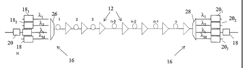
Optical systems 10 of the present invention include
optical amplifiers 12 disposed along an optical path 14
to optically amplify optical signals passing through an
optical link 15 between optical processing nodes 16. One
or more transmitters 18 can be included in the nodes 16
and configured to transmit information via the optical
signals in one or more information carrying signal
wavelengths, or signal channels, a,ei to one or more
optical receivers 20 in other nodes 16. The optical
system 10 can be configured in multi-dimensional networks
(Fig. 1) or in one or more serially connected point to
point links 15 (Fig. 2), which can be controlled by a
network management system 22.
In various network embodiments, such as in Fig. 1, a
signal channel a,ai can travel multiple paths, e.g., 14,
and 142, between an origination node 160 and a destination
node 16d. The signal channel also may have to traverse
one or more intermediate nodes 16i between the origination
node 160 and the destination node 16d.
The optical processing nodes 16 may also include one
or more other optical processing devices, for example,
integrated optical switching devices 24, such as optical
add/drop multiplexers and switches/routers/cross-
connects. For example, broadcast and/or wavelength
reusable, add/drop devices, and optical cross connect
switches and routers can be configured via the network
management system 22 in various topologies, i.e., rings,
mesh, etc. to provide a desired network connectivity.
The deployment of integrated switching devices 24 in
intermediate nodes 16i can provide all-optical
interconnections between the transmitters 18 and
receivers 20 in the origination node 160 and the
destination node 16d, respectively. In this manner, the
use of integrated switching device 24 in the system 10
- 7 -
CA 02414458 2003-01-06
WO 02/05462 PCT/US01/21471
provides for a distance independent all-optical network,
sub-network, or nodal connection.
The optical amplifiers 12 and optical processing
nodes 16 are referred to generally as network elements.
The optical path 14 extending between successive network
elements in the system 10 is referred to as a span.
Whereas, the optical link 15 extends between successive
nodes 16 and will include one or spans depending upon the
configuration of the system 10. For example, Fig. 2
shows a point to point optical link 15 including spans 1
through n.
The transmission media can include various guided
and unguided media, and is typically optical fiber 14.
Currently, the most commonly used optical fiber 14 in
optical transmission systems is a single mode fiber,
although multiple mode fibers can be used in various
applications. The optical fibers 14 can have various
dispersion and non-linear properties that affect the
transmission properties of the system 10. One or more
optical fibers 14 can be disposed to provide multiple
optical links 15 between nodes 16 along a common optical
path. In addition, each fiber can carry uni- or bi-
directionally propagating optical signals depending upon
the system 10 configuration.
The optical transmitters 18 and optical receivers 20
are configured respectively to transmit and receive
optical signals including one or more information
carrying optical signal wavelengths, or signal channels,
ksi= In the present description, the term "information"
should be broadly construed to include any type of
information that can be optically transmitted including
voice, video, data, instructions, etc.
The transmitters 18 used in the system 10 generally
will include a narrow bandwidth laser optical source,
such as a DFB laser, that provides an optical carrier.
The transmitters 18 also can include other coherent
narrow or broad band sources, such as sliced spectrum or
fiber laser sources, as well as suitable incoherent
- 8 -
CA 02414458 2003-01-06
WO 02/05462 PCT/US01/21471
optical sources as appropriate. Information can be
imparted to the optical carrier either by directly
modulating the optical source or by externally modulating
the optical carrier emitted by the source.
Alternatively, the information can be imparted to an
electrical carrier that can be upconverted onto an
optical wavelength to produce the optical signal. The
information can be amplitude, frequency, and/or phase
modulated using various formats, such as return to zero
("RZ"), non-return to zero ("NRZ"), differential phase
shift keying ("DPSK"), etc., encoding techniques, such as
forward error correction ("FEC"), etc., and transmission
protocols, such as SONET/SDH, IP, ATM, Ethernet, Fiber
Channel, etc.
The optical receiver 22 used in the present
invention can include various detection techniques, such
as coherent detection, optical filtering and direct
detection, and combinations thereof. The receivers 22
can be deployed in modules that have incorporated
wavelength selective filters to filter a specific channel
from a WDM signal or channel filtering can be performed
outside of the receiver module. It will be appreciated
that the detection techniques employed in the receiver 22
will depend, in part, on the modulation format used in
the transmitter 20. Also, various transmission formats
and protocols can be used within a WDM system, as well as
in each serial WDM or SDM link of transmitters 18 and
receivers 20.
Generally speaking, N transmitters 18 can be used to
transmit M different signal wavelengths to J different
receivers 20. Also, tunable transmitters 18 and
receivers 20 can be employed in the optical nodes 16 in a
network, such as in Fig. 1. Tunable transmitters 18 and
receivers 20 allow system operators and network
architects to change the signal wavelengths being
transmitted and received in the system 10 to meet their
network requirements. In addition, the transmitters 18
and receivers 20 can employ various feedback loops to
- 9 -
CA 02414458 2003-01-06
WO 02/05462 PCT/US01/21471
control the transmission characteristics of the signals
and configuration of the system 10.
The transmitters 18 and receivers 20 also can
include various components to perform other signal
processing, such as reshaping, retiming, error
correction, differential encoding, regeneration,
dispersion and distortion compensation, etc. For
example, receivers 20 can be connected to the
transmitters 18 in back to back configuration as a
regenerator, as shown in Fig. 2. The regenerator can be
deployed as a 1R, 2R, or 3R regenerator, depending upon
whether it serves as a repeater (reshape), a remodulator
(reshape & retime), or a full regenerator (reshape,
retime, regenerate), respectively.
In a WDM system, the transmitters 18 and receivers
can be operated in a uniform manner or the
transmission and reception characteristics of the signal
channels can be tailored individually and/or in groups.
For example, pre-emphasis, optical and/or electrical pre-
20 and post-dispersion and distortion compensation can be
performed on each channel or groups of channels.
In Fig. 2, it will be appreciated that the
transmitters 18 and receivers 20 can be used in WDM and
single channel systems, as well as to provide short,
intermediate, and/or long reach optical interfaces
between other network equipment and systems. For
example, transmitters 18 and receivers 20 deployed in a
WDM system can be included on a module that also includes
standardized interface receivers and transmitters,
respectively, to provide communication with interfacial
devices 25, as well as other transmission and processing
systems.
Interfacial devices 25, such as electrical and
optical cross-connect switches, IP routers, ATM switches
SONET ADMs, etc., can be used to provide various signal
processing and cross-connect functions at network
interfaces. The network interfaces occur at the
intersection point to point links and/or networks. When
the interfacial devices interconnect point to point
10 -
CA 02414458 2003-01-06
WO 02/05462 PCT/US01/21471
links, the network interfaces are in the core of an
opaque network as shown in Fig. 2. Whereas, the
interfacial devices 25 connect to the periphery of, or
edge, of a network, such as metropolitan, access,
regional, national, and/or multidimensional all-optical
networks, as shown in Fig. 1.
The interfacial devices 25 can be configured to
receive, convert, aggregate, groom, and provide
information via signaling or otherwise in one or more
various protocols, encoding schemes, and bit rates to the
transmitters 18, and perform the converse function for
the receivers 20. For example, interfacial devices 25
that perform electrical processing, such as electrical
cross connect switches, IP routers, etc., could be used
to aggregate STS-1 traffic up to OC-48 through OC-768 or
OC-768 traffic could be dissembled and groomed at lower
bit rates.
Interfacial devices 25 with optical switching
provide an automated patch panel function interconnecting
link and network interfaces to provide flexibility in
wavelength and path assignment for signal channels
traversing the interface. It will be appreciated that
any signal can be assigned different WDM wavelengths at
an interface, which is sometimes referred to as
wavelength conversion or grooming. Similarly, protection
and restoration switching at the interface does not
require that the same WDM wavelength be used on each side
of the interface or path.
The interfacial devices 25 can have electrical
input/output interface that can be connected to other
networks or interfacial devices 25. In addition, the
interfacial devices 25 can include optical input/output
ports, such as integrated WDM transmitters 18 and
receivers 20 and/or short, intermediate, and/or long
reach optical interfaces, typically operating in the 1300
nm or 1550 nm range.
The interfacial devices 25 also can be used to
provide protection and restoration switching in various
nodes 16 depending upon the configuration. Linear and
- 11 -
CA 02414458 2003-01-06
WO 02/05462 PCT/US01/21471
mesh protection restoration schemes can be implemented
using the interfacial devices'25. For example, various
protection schemes, such as 2&4 fiber BLSR, UPSR, 1+M,
M:N, etc. can be used alone or in combination with
various partial and full mesh restoration schemes.
Various types of optical switching devices 24, both
optical switches and OADMs, can be integrated into the
network to provide all-optical networking functionality
at the nodes 16 and the deployment of distance
independent networks. The switching devices 24 allow for
integrated optical switching, adding, dropping, and/or
termination of signal channels from multiple paths 14
entirely in the optical domain without the need for
receivers 20 and transmitters 18 to perform electrical
conversions, as required when using interfacial devices
to perform these functions. As such, signal channels
can optically pass through intermediate nodes 16;, between
the origin nodes 16o and destination nodes 16d channels,
optically bypassing the need for transmitters 18 and
20 receivers 20 at the intermediate nodes 16i. Optical
bypass at nodes 16 including switching devices 24
provides transparency through the node that allows all-
optical express connections to be established between
non-adjacent origin and destination nodes in a network.
25 As depicted in Fig. 1, integrated switching device
24 can be deployed at origination nodes 160 and
destination nodes 16d with transmitters 18 and receivers
20, respectively. The use of integrated switching device
24 in this configuration allows for transmission and
reception of signal channels X1 without terminating the
optical path using receivers 20 and transmitter 18 as is
the case in point to point links, as shown in Fig. 2.
Thus, transmitters 18 in the origination nodes 160 can
communicate with receivers 20 in via the optical paths 14
through the integrated switching devices 24 without
having to convert information between optical signals and
electrical signals merely to pass the information through
the nodes 16.
- 12 -
CA 02414458 2003-01-06
WO 02/05462 PCT/US01/21471
It will be appreciated that signal channels that are
switched onto a common path by the switching devices 24
from different paths can have different properties, such
as optical signal to noise ratio. Conversely, signal
channels entering the switching devices 24 from a common
path and exiting the devices 24 via different paths may
require that the signal channels exit with different
properties, such as power level. As such, signal
channels may have different span loss/gain requirements
or tolerances within the link 15.
The switching devices 24 can be configured to
process individual signal channels or signal channel
groups including one or more signal channels. The
switching devices 24 also can include various wavelength
selective or non-selective switch elements, combiners 26,
and distributors 28. The transmitters 18 and receivers
can be configured to transmit and receive signal
channels dynamically through the switch elements or in a
dedicated manner exclusive of the switch elements using
20 various combiners 26 and distributors 28. The OADMs can
include wavelength reusable and non-reusable
configurations. Similarly, the switching devices 24 can
be configured to provide multi-cast capability, as well
as signal channel terminations.
The switching devices 24 can include various
configurations of optical combiners 26 and distributors
28, such as multiplexers, demultiplexers, splitters, and
couplers described below, in combination with various
switch elements configured to pass or block the signals
destined for the various other nodes 12 in a selective
manner. The switching of the signals can be performed at
varying granularities, such as line, group, and channel
switching, depending upon the degree of control desired
in the system 10.
The switch element can include wavelength selective
or non-selective on/off gate switch elements, as well as
variable optical attenuators having suitable extinction
ratios. The switch elements can include single and/or
multiple path elements that use various techniques, such
- 13 -
CA 02414458 2010-05-20
as polarization control, interferometry, holography, etc. to
perform the switching and/or variable attenuation function.
The switching devices can be configured to perform various
other functions, such as filtering, power equalization,
dispersion compensation, telemetry, channel identification,
etc., in the system 10.
Various non-selective switch elements can be used in
present invention, such as mechanical line, micro-mirror and
other micro-electro-mechanical systems ("MEMS"), liquid
crystal, holographic, bubble, magneto-optic, thermo-optic,
acousto-optic, electro-optic (LiNbO3), semiconductor, erbium
doped fiber, etc. Alternatively, the switch elements can
employ fixed and tunable wavelength selective multi-port
devices and filters, such as those described below.
Exemplary switching devices 24 are described in PCT
Application No. PCT/USOO/23051.
Optical combiners 26 can be provided to combine optical
signal channels X from different optical paths onto a
common path, e.g. fiber. Likewise, optical distributors 28
can be provided to distribute optical signals from a common
path to a plurality of different optical paths. The optical
combiners 26 and distributors 28 can include wavelength
selective and non-selective ("passive") fiber, planar, and
free space devices, which can be polarization sensitive or
insensitive. Passive or WDM couplers/splitters, circulators,
dichroic devices, prisms, gratings, etc. can be used alone,
or in combination with various tunable or fixed, high, low,
or band pass or stop, transmissive or reflective filters,
such as Bragg gratings, Fabry-Perot, Mach-Zehnder, and
dichroic filters, etc. in various configurations of the
optical combiners 28 and distributors 28. Furthermore, the
combiners 26 and distributors 28 can include one or more
serial or parallel stages incorporating various devices to
multiplex, demultiplex, and multicast signal wavelengths Aei
in the optical systems 10.
-14-
CA 02414458 2010-05-20
As shown in Figs. 1 and 2, optical amplifiers 12 can be
disposed along the transmission fiber 14 to overcome
attenuation in the fiber 14 and proximate the optical
processing nodes 16 to overcome loss associated with the
nodes 16, as required. The optical system 10 can include one
or more amplifier types, such as various lumped and/or
distributed doped and/or non-linear fiber amplifiers, such
as erbium and Raman amplifiers, that can be supplied locally
and/or remotely with optical power, as well as other
amplifier types, e.g. semiconductor. The amplifiers 12 can
be deployed in serial and/or parallel stages 12i and in
combination with filters, attenuators, isolators, dispersion
compensating devices, and other signal varying devices, as
well as add/drop and other optical processing devices,
disposed between amplifier stages 12i and before and/or after
the amplifier 12. Exemplary amplifiers 12 are described in
U.S. Patent No. 6,115,174.
In addition, the amplifiers 12 can be locally and/or
remotely controlled using various automatic gain and/or
power control schemes depending upon the configuration of
the system 10. For example, U.S. Patent No. 6,236,487
describes various local control schemes, as well as
combination with remote control schemes to control a chain
of optical amplifiers.
As shown in Fig. 3, the optical amplifiers 12 generally
include an optical amplifying medium 30 supplied with power
from an amplifier power source 32. Optical signals passing
the amplifying medium are optically amplified by the medium
using energy supplied from the power source 32.
30 As shown in Fig. 4 and for the sake of clarity, the
optical amplifier 12 will be described further in terms
of an amplifying fiber 34 supplied with power in the form
of optical, or "pump", energy from one or more pump
sources 36. However, it will be appreciated that optical
amplifiers 12 including other amplifying media 30, i.e.,
-15-
CA 02414458 2003-01-06
WO 02/05462 PCT/US01/21471
semiconductor, etc., may be substituted with appropriate
modification, as previously mentioned.
The amplifying fiber 34 will generally be a doped
fiber and/or a fiber suitable for producing non-linear
interactions, such as stimulated Raman scattering, that
can be used to amplify optical signals. The optical
fiber 34 will be supplied with optical energy in one or
more pump wavelengths a,pi that is used to amplify the
signal wavelengths a,si passing through the amplifying
fiber 34. One or more dopants can be used in the doped
amplifying fiber 34, such as Er, other rare earth
elements, e.g., Yb and Nd, as well as other dopants. The
doped and Raman amplifying fibers 34 can be distributed
as part of the transmission fiber 14, or
concentrated/lumped at discrete amplifier sites, and can
be locally or remotely pumped with optical energy.
The amplifying fiber 34 can have the same or
different transmission and amplification characteristics
than the transmission fiber 14. For example, dispersion
compensating, zero and non-zero dispersion shifted, non-
dispersion shifted ("standard"), polarization maintaining
fiber and other fiber types can be intermixed as or with
the transmission fiber 14 depending upon the system
configuration. Thus, the amplifying fiber 34 can serve
multiple purposes in the optical system, such as
performing dispersion compensation and different levels
of amplification of the signal wavelengths Xi.
The pump source 36 can include one or more narrow
band or broad band optical sources 38, each providing
optical power in one or more pump wavelength ranges
designated by center pump wavelengths a,pi and including
one or more modes. The optical sources 38 can include
both coherent and incoherent sources, which can be
wavelength stabilized and controlled by providing, for
example, a Bragg grating or other wavelength selective,
reflective element in a pig tail fiber of the source. A
portion of the pump power can be tapped to an O/E
- 16 -
CA 02414458 2003-01-06
WO 02/05462 PCT/US01/21471
converter and an optical source controller employed to
provide feedback control over the optical source.
Various configurations of combiners 26, as
previously described, can be used to combine pump
wavelengths ?,pi for introduction in the amplifying fiber
34. Pump energy can be supplied to the amplifying fiber
34, either counter-propagating and/or co-propagating with
respect to the propagation of the signal wavelengths k .
It will be appreciated that in a bi-directional amplifier
12, the pump wavelengths ),pi will be counter-propagating
relative to signal wavelengths 2 in one direction as
well as co-propagating relative to signal wavelengths
in the other direction.
In the present invention, the gain of each
individual amplifier 12 in the link 15 is not adjusted to
compensate for the loss in an associated span, i.e.,
Amplifier Gain # Span Loss. In other words, various
spans in the system 10 are not operated at transparency,
but with a net loss or a net gain depending upon whether
the amplifier 12 provides gain that is greater than or
less than their respective span losses. However, the
amplifiers 12 in the optical link 15 are operated, such
that the cumulative gain of the amplifiers 12 compensates
for the cumulative loss in the link 15. Unlike prior
systems, each span in the present invention is not
operated transparently, but multiple spans are operated
so that the cumulative span is operated transparently.
By allowing net gain and net loss variations in
individual spans, but maintaining cumulative
transparency, over a plurality of spans, the system can
be operated using optical amplifiers that provide
different levels of amplifier and system performance,
such as noise figure, gain margin, and spectral gain
profile, etc. For example, high gain, high noise figure
amplifiers can be replaced by lower gain, lower noise
figure amplifiers, which can improve the performance of
the system. Net losses incurred in spans, in which lower
- 17 -
CA 02414458 2003-01-06
WO 02/05462 PCT/US01/21471
gain amplifiers were deployed can be offset by operating
one or more of the other amplifiers to provide a net
gain.
While various types of optical amplifiers can be
used in the system as previously described, each type of
amplifier does not have the same gain versus other
amplifier performance characteristics, such as noise
figure, spectral gain profile, etc. For example,
distributed amplifiers generally can provide a lower
noise figure for a given amount of gain than is provided
using a concentrated amplifier, assuming comparable
levels of amplified spontaneous emissions are produced by
both amplifiers.
The operation of spans with net gain and loss
effectively creates a virtual amplifier spacing, in which
the gain of the amplifiers in the plural spans is based
not on the actual span losses in a network. Instead, the
gain of the amplifiers is established based on required
cumulative gain required to overcome the cumulative span
loss and various type of amplifiers and amplifier gain
required to achieve a desired level of performance in the
system.
In various embodiments, two or more of the optical
amplifiers 12 in the optical link 15 are operated such
that the signal power at the output of the amplifier 12
varies from a nominal output signal power. The
respective spans are operated with net gains and losses,
while the link 15 is operated transparently and the
signal power at the end of the link 15 is equal to the
nominal output signal power.
In the present invention, plural spans can be
operated, such that the nominal signal power at the input
to the plural spans can be different from the nominal
signal power at the output of the plural spans. For
example, if optical signals are transmitted or launched
at different nominal signal power than the signal are
received or otherwise processed or when varying fiber
types are used. In those embodiments, cumulative
18 -
CA 02414458 2003-01-06
WO 02/05462 PCT/US01/21471
transparency is provided relative to the nominal signal
input and output powers.
As shown in Figs. 5a and 5b, the maximum and minimum
signal channel power varies from span to span. However,
at span n, the signal power at the output of the optical
amplifier is at the nominal output signal power to
provide cumulative transparency through the plural spans.
As further shown in Fig. 5b, in various embodiments,
the cumulative net gain or loss can be established and
monitored, if necessary, such that the cumulative net
gain or loss is constrained between a maximum net gain
and a maximum net loss range during transmission. The
cumulative range constraints can be used to prevent the
signal powers from becoming too high or too low along any
span during transmission, while cumulative transparency
is maintained at the end of the spans. The maximum net
gain and maximum net loss values can be set based on
various factors, such as optical signal to noise ratio
and non-linear interaction limits.
As shown in Fig. 6, in various embodiments employing
multiple fiber types, it is possible to vary the nominal
output signal power depending upon the fiber type. The
present invention allows for net gain or loss variations
to be propagated through multiple fiber types to more
evenly control the signal power profile through a
plurality of spans/amplifiers.
While Fig. 5a-6 depict signal channel power profile
of a single or average channel along the span, it will be
appreciated that each signal channel ki being transmitted
through the system 10 can have the same or different
profile as some or all of the other channels. For
example, in some spans all channels can experience a net
gain or net loss of signal power; whereas, in other
spans, different channels can experience net gain, net
loss, and transparent operation.
Cumulative transparency can be established as a
condition to be achieved at the end of the link 15 or at
some intermediate point in the link 15 after a plural
- 19 -
CA 02414458 2003-01-06
WO 02/05462 PCT/US01/21471
number of spans. Additional rules can be generated to
constrain the maximum number of spans over which a net
gain and/or net loss can be maintained in the link 15.
In operation, signals at the output of each
amplifier can be at different power levels, which is
contrary to prior art systems that provide for constant
signal powers at the amplifier output. Each amplifier 12
can be configured to operate at a fixed and programmable
signal output power set point, which can be manually or
automatically set, either locally or remotely, such as
via the NMS 24. The system 10 also can be used with
different fiber types that can support different signal
power levels within the system 10.
In practice, cumulative transparency can be taken
into account in the design of the system 10. For
example, it may be more desirable to place higher gain
amplifiers in some spans to allow lower gain amplifiers
in other spans. Likewise, various types of amplifiers
12, such as concentrated and distributed doped and Raman
fiber amplifiers, can be deployed effectively to provide
cumulative transparency, but not necessarily transparency
over every span, or "span transparency".
In addition, the present invention can be used to
ameliorate the effects of amplifier failures in the
system. For example, the failure of one or more pump
sources providing energy to optical amplifying media can
result in degraded performance of the amplifier and
overall net loss for the span or spans in which the
failures occur. In the present invention, the non-failed
amplifiers can provide additional redundancy to offset
the failure by being configured to operate the
corresponding spans at a net gain, and, thereby maintain
cumulative transparency over plural spans and/or the
link.
In various embodiments, the gain provided by each
amplifier can be controlled locally using various gain
and power control schemes. In addition, control over
multiple spans can be provided to allow the gain or power
set points to be reconfigured manually or automatically
- 20 -
CA 02414458 2003-01-06
WO 02/05462 PCT/US01/21471
via local or remote network management to adjust for
variations in the performance of plural spans, so as to
maintain cumulative transparency in the system 10.
Generally, the network management system 22 provides
for management at the network element level and at the
network level. The network management system 22 can
include software that is run on dedicated or shared
processors provided in, for example, stand-alone or
network computers, such as at the network or network
element level, that access the software on a fixed or
removable dedicated or shared memory or data storage
devices, such as compact or floppy discs, hard drives,
read-only memory, etc. In addition, the NMS 22 can
include software that is resident in a central processor
memory and executed by the central processor, such as in
network elements.
The present invention can be implemented using
software implemented at various levels in the network
management system 22. For example, the network
management system 22 can include a network planning
software application that determines the amplifier gain
required for amplifier 12 provided along the plural spans
being planned based on the cumulative loss calculated
from the individual span losses. To further the example,
the network planning application can specify the type of
amplifier 12 to install in the network to provide a
desired level of performance and cost based on the
individual and cumulative span losses. The selection of
amplifiers 12 can be governed by various rules pertaining
to the nominal signal powers, maximum net gain, maximum
net loss, etc.
Generally, the NMS 22 can include a computer
readable medium that contains a set of instruction that
when executed adjusts the gains amplifier of the optical
amplifiers provided along the spans to compensate for the
cumulative loss in the plurality of spans. In addition,
the NMS 22 can adjust the gain of at least two of the
optical amplifiers to provide net gain and/or net loss in
those individual spans. The instructions can be
- 21 -
CA 02414458 2003-01-06
WO 02/05462 PCT/US01/21471
executable from the network element and/or the network
levels. For example, the nodes 16 can include NMS 22
processors that controls the gain set points for some or
all of the amplifiers 12 in the links 15 connecting to
the nodes 16. In addition, the nodes 16 can send
instructions to processors in the individual amplifiers
via a system supervisory channel to perform the amplifier
gain adjustments.
The impact of cumulative transparency in an all-
optical network, sub-network, or nodal connection will
depend upon the variations in signal characteristics of
the signal channels travelling diverse paths. In various
embodiments, the maximum net loss of a span can be
defined based on various characteristics, OSNR,
accumulated dispersion, non-linear interactions, etc., as
the signal channels traverse the all-optical portion of
the network.
Cumulative transparency can be extended from a
signal channel origin node 16o to the destination node 16d
through one or more transparent intermediate nodes 16i,
when all-optical switching devices 24 are deployed in the
intermediate nodes 16i. Cumulative transparency can be
applied on any number of bases from individual channels
up to all channels in the system 10 over two or more
spans within a link or one or more links.
Unlike point to point link embodiments, in which
links are defined by the origination and termination of
optical signals, cumulative transparency can be defined
between any two points in the network. When cumulative
transparency is defined over multiple links, each link
may be operated at a net gain or net loss depending upon
the characteristics of the links. For example, links
that include larger core fibers may be operated at higher
signal channel powers than links containing smaller core
fibers. As such, the signal channel power launched into
one link may be different from the signal channel power
exiting the link and entering another link.
Alternatively, the signal channel power can exit the
fiber at the same power as it was launched, but the node
22 -
CA 02414458 2003-01-06
WO 02/05462 PCT/US01/21471
16 can be operated at a different power level than any of
the links connected to the node 16.
It will be appreciated that the present invention
provides for optical systems with improved performance.
Those of ordinary skill in the art will further
appreciate that numerous modifications and variations
that can be made to specific aspects of the present
invention without departing from the scope of the present
invention. It is intended that the foregoing
specification and the following claims cover such
modifications and variations.
- 23 -