Note: Descriptions are shown in the official language in which they were submitted.
CA 02414465 2002-12-16
Doc. No: LO-573 CA Patent
OPTICAL TRANSMITTER
Field of the Invention
[O1] The present invention relates to an optical transmitter for use in
optical communications systems,
and more particularly to an optical transmitter apparatus having an
interferometric modulator
external to the light source and a method for its control.
Background of the Invention
[02] Optical transmitters with interferometric external modulators typically
include a laser diode
source of optical power and a controllable interferometer. The output of the
laser diode is stabilized
in wavelength and power. Light emitted from the laser diode is incident on the
controllable
interferometer, such as a Mach-Zehnder interferometer consisting of a
branching optical waveguide
for separating the light to be modulated into two portions of substantially
equal power, coupled to
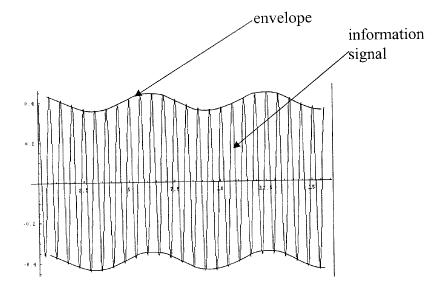
two optical paths leading from the branching device. The two optical paths are
generally of
essentially the same physical length. One or both of them is provided with a
means to modulate its
optical length. The two paths are coupled at their output ends to a combining
device for recombining
into a single output the light that has passed each path. Such Mach-Zehnder
modulators are usually
configured as waveguides in an electro-optical material in which the optical
path length through a
waveguide section can be controlled by means of the sensitivity of the
material's refractive index to
an applied electric field. Lithium niobate or various compositions of
quaternary semiconductors that
may be compatible with the fabrication of the laser itself are materials
commonly used. Diffused or
ridge waveguide structures may be used. The electric field for controlling
optical path length results
from a voltage signal applied to an electrode or electrodes associated with
the two optical paths
between the branching and combining devices. It is known that in modulator
devices of this type, the
modulation of the optical path can be arranged to yield no wavelength chirping
or a desired form and
degree of wavelength chirping.
[03] Typically the signal with which the light is to be modulated is binary
and consists of two voltage
levels. It is desirable to obtain the greatest possible ratio of transmissions
between the transmissive
and non-transmissive states of the modulator (extinction ratio) in order that
the modulation of the
light be as great as possible. In order to obtain maximum extinction ratio,
one of the applied voltage
CA 02414465 2002-12-16
Doc. No: 10-573 CA Patent
levels should be near the voltage that yields maximum transmission and the
other near the voltage
yielding minimum transmission through the interferometer. The applied digital
signal will then have
an average voltage that is near the middle of the voltage - transmission
characteristic of the
interferometer. This average voltage is called the "bias point". If analog
rather than digital signals
are to be transmitted, the bias point corresponds to the average voltage in
the signal and the
maximum and minimum transmission voltages correspond to the peaks of the
applied signal.
[04] The modulation transfer function of a typical interferometric modulator
is shown in Fig 1 with
the bias point indicated and the mapping between a typical digital input
voltage signal and output
optical signal shown. It is important to note that the transfer function is
periodic in voltage because
the interferometer cycles through more than one order of interference as the
drive voltage is
monotonically increased. The shape of the transfer function is sinusoidal in
principle. In
consequence of this periodicity, there is an approximately linear portion of
the transfer function
containing the bias point, but at voltages sufficiently far from the bias
point the sensitivity of the
optical modulation to applied voltage abates, passes through zero, and
reverses sign.
[OS] One known difficulty of interferometric modulators is the problem of
ensuring that the average
of the modulation signal corresponds to the best bias point for the modulator.
With temperature,
aging and other effects the voltage that corresponds to the optimum bias point
may shift. It is
desirable to provide a method whereby the modulation performance of the
transmitter can be
monitored and the bias voltage corrected if need be. Such a system is
described in US Patent
5,170,274 assigned to Fujitsu Ltd., Kawasaki, Japan, and reissued as Re
36,088, which are
incorporated by reference herewith. It is shown in these patents that the bias
can be maintained at a
correct level by monitoring a small, periodic signal which shall be referred
to as the "dither" signal
that is imposed on the information signal to be transmitted before it in turn
is applied to the
modulator to generate the optical signal. The result is a voltage signal that
consists of the signal to
be transmitted, with a small modulation of its envelope consisting of the
dither signal. The dither
signal modulates the information signal so that each side of the envelope of
the information signal is
varied at equal amplitudes and in opposite phases to correspond to the dither
signal , as shown in Fig.
2. This composite signal is applied to the modulator, imposed on the light,
detected by tapping off a
portion of the modulated light, and monitored in the output of an optical
receiver that receives the
tapped light.
2
CA 02414465 2002-12-16
Doc. No: IO-573 CA Patent
[06] When the bias is correct the monitored signal does riot contain a
component at the dither
frequency because the average power of the optical signal is constant.
However, if the bias voltage is
too high, the modulation of the upper side of the information signal envelope
is far enough from the
bias point to be reduced or even inverted in polarity, following the
nonlinearity of the transfer
function in this region. In such a situation the monitor signal does contain a
component at the dither
frequency. Hence the presence of a dither component in the monitor signal
indicates that a
correction should be made to the bias voltage. If the bias voltage is too low,
the dither signal on the
lower side of the envelope is compressed or inverted and in this situation too
there is a component in
the monitor signal at the dither frequency. It is in opposite phase by
comparison with the situation
when the bias point is loo high, thus there is a means of knowing in what
direction the correction to
the bias voltage should be made. The presence of the dither component in the
monitored signal and
its polarity can be detected by homodyne detection whereby the monitor signal
is multiplied by the
dither signal. The presence of a dither component is indicated by a constant
voltage from the
homodyne process, with the polarity of the voltage indicating the polarity of
the dither component.
[07] While the method described in US Patent 5,170,274 succeeds in providing a
monitoring signal
that indicates a bias error and a direction for the bias correction, it
suffers from complexity of
implementation. The dither signal must be imposed on the information signal in
such a way that the
two sides of the signal envelope are of equal amplitudes and in antiphase. The
simplest method
consists of adding the dither signal to a constant voltage and multiplying the
result with the
information signal. Electronic multiplying circuits for adding the dither
signal to a bias and
multiplying it with the information signal are required in addition to the
Mach-Zehnder driver
amplifier and the dither signal generation circuit.
[08] It is an object of this invention to provide a simpler method and
apparatus for introducing a
monitoring signal on an optical information signal for maintaining the correct
bias condition of an
interferometric modulator.
[09] It is an object of this invention to eliminate the need for electronic
multipliers. In one
embodiment, the monitor signal can be applied simply by means of a second
drive electrode in the
Mach- Zehnder interferometer.
Summary of the Invention
3
CA 02414465 2002-12-16
Doc. No: 10-573 CA Patent
( 10] In accordance with one aspect of the invention, there is provided an
optical modulator
comprising:
( 11 ] an optical interferometer having first and second branch paths between
and optically coupled
with an input port and an output port;
[ 12] first electronic means for varying an optical path length between the
input port and the output
port in dependence upon an information signal;
13] second electronic means of varying an optical path length between the
input port and the output
port in dependence upon a dither signal;
14] wherein variations of optical path length produced by first electronic
means and second
electronic means combine linearly to produce a net phase difference after
combining.
[ 15] In accordance with another aspect of the invention, there is provided a
method of controlling a
modulator having control circuitry, the method comprising the steps of:
[ 16] providing a dither signal to one of the modulator and control circuitry
coupled to the modulator;
[I7] providing an information signal to one of the modulator and control
circuitry coupled to the
modulator, summing the dither signal and an information signal to yield a
control signal; and,
[18] utilizing at least a portion the control signal to control the modulator
in a feed-back loop.
Brief Description of the Drawings
(19] Exemplary embodiments of the invention will now be described in
conjunction with the drawings
in which:
[20j Fig. 1 illustrates the modulation transfer function of a conventional
interferometric modulator,
[21 ] Fig. 2 illustrates the modulation of the information signal by a dither
signal according to the prior
art wherein each side of the information signal envelope is varied in opposite
phases,
[22] Fig. 3 represents a combination of the information signal with the dither
signal according to the
present invention,
[23] Figs. 4a-4c show voltage waveforms of the monitored signal according to
the invention,
respectively when the bias is too high (Fig. 4a), at correct bias (Fig. 4b)
and when the bias is too low
(Fig. 4c),
[24] Figs Sa-Sc show voltage waveforms produced by the monitor receiver after
highpass filtering that
excludes signal components in the range of the dither signal, respectively for
bias too high (Fig. 5a),
bias correct (Fig. 5b) and bias too low (Fig. 5c),
4
CA 02414465 2002-12-16
Doc. No: 10-573 CA Patent
[25] Fig. 6 illustrates an amplitude demodulation circuit of the highpass
filter of rectify-and-integrate
type that can process the monitor signal to obtain waveforms that can be used
for bias correction,
[26] Fig. 7 shows the outputs of the circuit of Fig. 6 for bias too high, bias
correct, and bias too low,
[27] Fig. 8a illustrates a Mach Zehnder interferometer having input terminals
on which to apply a
voltage arranged in series along a same waveguide;
(28] Fig. 8b illustrates a Mach-Zehnder interferometer having input terminals
on which to apply a
voltages arranged along different waveguides; and
[29] Fig. 8c illustrates a modulator wherein an information signal and a
periodic dither signal are
added together and subsequently provided as a summed voltage signal to a pair
of terminals on of the
waveguides of the interferometer.
Detailed Description of the Invention
[30] In the inventive method and apparatus for maintaining correct bias, a
dither signal is introduced
into the optical signal that is output from the modulator. This composite
signal is detected by tapping
off a portion of the modulated light, and monitored in the output of an
optical receiver that receives
the tapped light. By suitable processing of the detected portion of the signal
output from the
modulator the information required to determine whether the bias is correct,
and how to alter the bias
voltage if it is not, is obtained and used to control the bias voltage.
[31] Contrary to prior art, the dither signal is imposed on the optical
information signal in such a way
that the envelope is modulated in the same phase at both its upper and lower
edges, as shown in Fig.
3. Such a modulation can be obtained by adding the dither signal to the
information signal rather
than by modulating the information signal with the dither signal as in prior
art. The process of
addition can be performed electronically and the sum of the two signals can be
applied to the
modulator as a single drive signal. Alternatively, and more simply, the dither
signal can be
separately applied to the modulator in such a way that the phase shifts
induced by the signal and
dither have a linearly combined effect on the phase shift induced in the two
paths of the
interferometer. Such a separate application of signals can be achieved, for
example, by applying the
signals to separate electrodes.
(32j When the bias point is correct the information component in the monitored
signal varies around
an average power level that moves up and down sinusoidally at the dither
frequency. When the bias
CA 02414465 2002-12-16
Doc. No: 10-573 CA Patent
point is too high, the information waveform is clipped or even inverted at its
upper levels by the
nonlinearity of the modulator response. When the bias point is too low, the
information waveform is
clipped or inverted at its lower levels. Notably, the clipping of the
information waveform at high or
low levels occur at different times, corresponding to opposite phases of the
dither signal. This
difference permits the identification of the sign of the error in the bias
voltage after appropriate
signal processing. Voltage waveforms of the monitored signal are shown in
Figs. 4a - 4c for the
case of bias being too high (Fig. 4a), correct (4b) and too low (4c).
[33] The monitored voltage waveforms such as shown in Figs. 4a-4c are
subjected to highpass
filtering that excludes components in the range of the dither signal. The
variations in the average
level are removed but variations of the peak heights of the data signal that
result from clipping are
retained. These resulting signals constitute amplitude modulation signals in
which amplitude
modulation results directly from the nonlinearity of the modulator, in
contrast to the amplitude
modulation signals of prior art, which are generated before the modulator.
Monitor signals 4, 5 and
6 that correspond to signals 1, 2 and 3 after highpass filtering are shown in
Fig. 5. Waveform 5 is the
signal when the bias is correct, yielding substantially constant peak heights,
waveform 4 shows the
variation of peak height when the bias is too high and clipping occurs at the
upper envelope, and
waveform 6 shows the filtered waveform when the bias is too low and the
clipping occurs at a
different phase of the dither signal.
[34] Signals such as shown in Figs. Sa-Sc 6 carry information about the bias
condition as amplitude
modulation. The information can be recovered from the highpass filtered
monitor signal by any of
several known methods for detecting amplitude modulation. Homodyne detection
against a signal at
the information frequency is one possibility. A more simple and practical
method is to rectify and
integrate the signal by a circuit of the type shown in Fig 6, the circuit
having a highpass filter 10, a
rectifying filter 12 and a lowpass filter 14. The output of such a circuit is
shown in Fig. 7 for the
three bias cases discussed above. If the bias is correct (8) the signal is
essentially constant at a
maximum average level (a small variation may occur at the information signal
rate). If the bias is
incorrect the signal has a lower average value and contains a component at the
dither frequency, in
one phase (7) for bias too high and the other (9) for bias too low. The phase
of the error signal can
be determined by comparison with the dither signal applied to the modulator.
6
CA 02414465 2002-12-16
Doc. No: 10-573 CA Patent
[35] The average value, modulation amplitude and phase of the dither signal
can be detected by
various methods of signal processing. Sampling this signal and digitally
determining average,
amplitude and phase is possible because the dither signal can be reasonably
slow. Alternatively,
homodyne detection of amplitude and phase of the dither signal in the output
of the monitor may be
used.
[36) The voltage bias of the optical modulator is correct if the component in
the monitor signal at the
dither frequency is minimal and the average value of the signal is maximal.
The bias should be
increased if the average drops below a threshold, and/or a component at the
dither frequency appears.
The bias should be increased if the phase of the dither frequency component
corresponds to an
insufficient bias condition, or reduced if the phase is opposite.
[37) The inventive method of combining the information signal and the dither
signal can be
accomplished by simpler components than needed for the prior art. Linear
combination, i.e. addition
or subtraction, of the information and dither signals is required. Such linear
combination can be
achieved by low frequency electronic circuits only capable of handling the
dither frequency without
the need for electronic multiplier circuits. For example, variation of the
modulator bias at the dither
frequency accomplishes this goal. Unlike the prior art the dither signal can
be applied to the
information signal directly in the optical modulator itself by including a
separate electrode or other
method of phase control that responds only to the dither. The addition of
phase differences applied
by two separate phase controllers will result in the linear combination of the
corresponding signals
appearing as the modulation on the light. This method considerably simplifies
the electronics
necessary for the control of bias point.
[38) Numerous other embodiments of the invention will occur to those skilled
in the art, and the
invention is to be defined solely by the appended claims.
7