Note: Descriptions are shown in the official language in which they were submitted.
CA 02414543 2002-12-13
7.168P20CA01
ELECTRONIC BALLAST SYSTEM HAVING EMERGENCY LIGHTING PROVISIONS
BACKGROUND OF THE INVENTION
1.0 Field of the Invention
This invention relates to electronic ballast systems, and, more particularly,
to an
electronic ballast system for operating fluorescent lamps with universal input
(from 108V
to 305V) and having a subsystem with a battery, along with a battery charger,
and
associated logic that provides for emergency lighting.
Z.0 Description of Related Art
Electronic ballast systems for operating fluorescent Iamps are well known and
some of which are disclosed in U.S. Patents 5,808,421 and 6,031,342.
Electronic ballast
systems typically convert a low frequency alternating current source having a
relatively
low frequency in the range from 50 to 60Hz to a higher frequency typically in
the range
of 30-40 kHz. The conversion commonly involves a two stage process, wherein
the ac
oscillation having a frequency of SO to 60Hz is first rectified to a do
voltage and then this
do voltage is chopped at a higher frequency to produce alternating current in
the
frequency range of 30-40 kHz, which is used to excite the fluorescent lamp.
The
electronic ballast circuits advantageously perform the desired function for
operating
fluorescent lamps and reduce the energy consumption, compared to non-
electronic ballast
circuits, and especially compared to incandescent lamps. However, the
conventional
electronic ballast circuits typically employ a preheat operating mode that
needs to be
completed before the fluorescent lamp is excited so as to sequence it into its
continuous
and efficient running mode. It is desired that an electronic ballast circuit
be provided that
CA 02414543 2002-12-13
eliminates the need for preheating the fluorescent lamp before the fluorescent
lamp is
rendered operative into its continuous operating and efficient running mode.
Electronic ballast circuits are typically selected to have parameters that
operate
for particular input frequency oscillation. For example, the electronic
ballast circuit may
have parameters selected so as to operate with the 110 volt, 60 Hz typically
found in the
United States, whereas other ballast circuits may have parameters selected to
operate with
220 volts, SO Hz typically found in European countries. It is desired to
provide a ballast
circuit that operates with the universal input covering the range from between
108 to 305
volts at a frequency range between 50-60 Hz.
Further, it is desired to provide an electronic ballast circuit that handles
various
types of fluorescent lamps such as, T5, T8, T12, 20W, 32W, 40W, ~6W, 70W,
linear,
circular, or U-shaped type fluorescent lamps.
Because fluorescent lamps have a lower energy consumption compared to
incandescent lamps, they are extensively used in industrial and commercial
environments, which commonly require emergency lighting. It is desired to
provide for
electronic ballast system for operating one or more fluorescent lamps and
having a
subsystem with a battery, along with a battery charger, and associated logic
to provide for
emergency lighting.
CA 02414543 2002-12-13
Electronic ballast systems that operate fluorescent lamps are commonly plagued
by the disadvantage that they produce electro-magnetic interference (EMI) and
radio
frequency interference (RFI). It is desirable to provide for an electronic
ballast system
that reduces or even eliminates the EMI/RFI noise commonly produced by the
electronic
ballast systems.
Electronic ballast circuits commonly employ inductive loads, which act to
lower
the power factor, which, in turn, increases the consumption of current and,
thereby,
reduces the efficiency related to fluorescent lamps. It is desirable that an
electronic
ballast circuit be provided with a power factor correction circuit that allows
for the
creation of a power factor that approaches unity, thereby furthering the
efficiency of the
electronic ballast system.
SUMMARY OF THE INVENTION
The invention is direct to an electronic ballast system for operating one or
more
fluorescent lamps with universal input (from 108V to 305V) and having a
subsystem
with a battery, along with a battery charger and associated logic, that
provides for
emergency lighting. The electronic ballast system allows for the operation of
fluorescent
lamps without preheating their cathodes, as well as a circuit for power factor
correction
that allows electronic circuit to have a power factor that approaches unity.
The electronic ballast system comprises: (a) an EMI filter having an input
connected to an electric surge and providing a filtered output; (b) a full-
wave rectifier
CA 02414543 2002-12-13
having an input connected to the output of said EMI filter and providing a
first d.c.
voltage; (c) a power factor correction circuit having an input connected to
the output of
the full-wave rectifier and providing a power factor regulated output; and (d)
a first
inverter ballast circuit having an input connected to the output of the power
factor
converter. The inverter ballast circuit has a sweep frequency circuit for
supplying an
oscillating current to power a first fluorescent lamp without the need of
preheating its
cathode.
BRIEF DESCRIPTION OF THE DRAWINGS
Fig. 1 is a block diagram of the electronic ballast system of the present
invention.
Fig. 2 is a schematic illustrating the EMI filter, rectifier, and power factor
correction (PFC) circuit of all of Fig. 1.
Fig. 3 is a schematic of the inverter ballast of Fig. 1.
Fig. 4 is a schematic of the switching power and battery charger of Fig. 1.
Fig. 5 is a schematic of the emergency section of Fig. 1.
DESCRIPTION OF THE PREFERRED EMBODTiI~ZENTS
With reference to the drawings, wherein the same reference number indicates
the
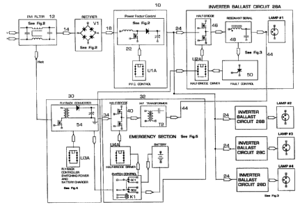
same element throughout, there is shown in Fig. 1 an electronic ballast system
10 for
operating one or more fluorescent lamps and having the capability of providing
for
emergency lighting.
a
CA 02414543 2002-12-13
The electronic ballast system 10 comprises an electromagnetic interference
(EMI)
filter 12 having input terminals L 1 and N, connected to a source of current,
and providing
a filtered output on signal paths 14 and 16. The electronic ballast system 10
further
comprises a full-wave rectifier V 1 having its inputs connected to signal
paths 14 and l6of
the EMI filter 12 and providing a first rectified d.c. voltage on signal paths
18 and 20 . A
power factor correction circuit 22 has its inputs connected to signal paths 18
and 20 of the
full-wave rectifier V 1 and provides a power factor regulated output on signal
paths 24
and 26.
The electronic power system further comprises a first inverter ballast 28A and
preferably further comprises three additional inverter ballast circuits 28B,
28C, and 28D.
Each of the inverter ballast circuits 28B, 28C, and 28D has their inputs
connected to the
signal paths 24 and 26 of the power factor correction circuit 22. Further,
each of the
ballast circuits 28A, 28B, 28C, and 28D has a sweep frequency circuit
supplying an
oscillating current to provide power to a fluorescent lamp into its operating
or running
mode without the need of first preheating the fluorescent lamp.
The electronic ballast system 10 has a capability of providing for emergency
lighting from a subsystem comprised of a switching power and battery charger
30 and an
emergency section 32.
CA 02414543 2002-12-13
The switching and battery charger 30 has a power supply having its inputs
connected across hot and ground terminals of the ENLI filter 12 and provides a
second d.c.
voltage having positive and negative potentials applied to signal paths 34 and
36,
respectively.
The emergency section 32 has a switch Kl allowing connection to the signal
paths 34 and 36 and has a plurality of contacts SC 1 and SC2. The emergency
section 30
further comprises a diode D16 having an anode and cathode with the anode
connected to
the positive potential on signal path 34. The emergency section 30 still
further comprises
a battery having positive and negative terminals with a negative terminal
connected, by
way of signal path 38, to the negative potential on signal path 36 and the
positive
terminal thereof connected to the cathode of the diode D 16.
The emergency section further includes a second ballast inverter comprised of
a
half bridve driver U4A, a half bridge arrangement 40, and a high voltage
transformer T2.
The second inverter circuit has an input and output arranged by means of the
plurality of
the sW tch contacts SC 1 and SC2 so as to interconnect the positive and
negative terminals
of the batter<~ when the second d.c. voltage normally applied across terminal
34 and 36 is
absent. The second inverter circuit has a sweep frequency circuit for
supplying an
oscillating current to a :first iluorescent'amp without the need of first
preheating the arse
~l~.:n~.: . =~: ...- :~ in a manner similar to that of inverter ballast
circuits 28A, 28B, 28C,
and 28D. The second inverter ballast circuit further comprises means, to be
discussed
CA 02414543 2002-12-13
with reference to Fig. 5, for energizing signal paths 42 and 44 so as to
excite the --
fluorescent lamp of the inverter ballast circuit 2~A.
The electronic ballast system 10, more particularly, the EMI filter 12 is
comprised
of a plurality of elements as listed in Table 1, and may be further described
with
reference to Fig. 2.
TABLE 1
Element Typical ValueJType
S 11 Conventional fuse
R 1 Varistor
C1 Film Capacitor (Interference
Suppressor)
C2 Film Capacitor (Interference
Suppressor)
C3 Film Capacitor (Interference
i Suppressor
L Common mode inductor
l
and
LZ
The purpose of the EMI filter 12 is to reduce or even eliminate the
electromagnetic interference (EMI) and radio interference (RFI) serving as
sources of
noise that would otherwise most likely be produced by the electronic ballast
system 10.
This electrical noise can interfere with the operation of televisions, radios,
telephones,
and similar equipment. Further, this electrical noise can be conducted through
power
lines which radiate and create disturbances in external equipment.
CA 02414543 2002-12-13
The EMI filter 12 is connected across the source of voltage which, because of-
benefits of the present invention, may vary from about 100 to 305 volts a.c.
with a
frequency variation between 50-60 Hz. The EMI filter 12 is comprised of the
common
mode inductors L 1 and L2, wound around the same core and operatively
connected to
capacitors C1, C2, and C3 arranged as shown in Fig. 1, and provides RFI/EMI
filtering of
common mode noise. Additionally, the EMI filter 12 includes a fuse SI1 that
provides
for over current protection and a varistor Rl that provides protection against
high voltage
spikes. The EMI filter 12 provides a filtered output on signal paths 14 and
16, which is
applied across a full-wave bridge rectifier V 1 comprised of conventional
diodes arranged
as shown in Fig. 2.
The full-wave bridge V 1 operates in a usual way to convert the filtered
output of
the EMI filter 12 into a d.c. voltage which is applied, via signal paths 18
and 20, across a
leveling capacitor C4, which is part of the power factor correction (PFC)
circuit 22
comprised of the plurality of elements given in Table ? and arranged as shown
in Fig. 2.
8
CA 02414543 2002-12-13
TABLE Z .-
Element Typical Value/T'ype
C4 Electrolytic Capacitor (Smoothing
Capacitor)
CS Film Capacitor
C6 Film Capacitor
C7 Electrolytic Capacitor
C8 Electrolytic Capacitor
C9 Electrolytic Capacitor
R2 Resistor
R3 Resistor
R4 Resistor
RS Resistor
R6 Resistor
R7 Resistor
R8 Resistor
R9 Resistor
R10 ~ Resistor
D 1 Diode Fast Recovery
D2 Diode Fast Recovery
D3 Boost diode
Q 1 Controlled power switch
T1 having winding T1A and T2A High Frequency Transformer
UlA ~ Power Factor Control
The purpose of the power factor correction circuit 22 is to derive a power
factor
for the electronic power system 10 that approaches unity. The power factor
correction
circuit 22 is preferred to be implemented into the electronic ballast system
10 because the
9
CA 02414543 2002-12-13
electronic ballast system 10, as well as all known ballast circuits, uses
inductors whicl3
tend to reduce the power factor as seen by the source of a.c. excitation
supplying the
electronic ballast system 10. This lowering of the power factor
disadvantageously
increases the consumption of power related to the fluorescent lamps and the
magnetic
ballast components. Typically this reduction in the power factor and related
inductive
disturbances creates a 40% increase in power consumption. The power factor
correction
circuit 22 of the present invention performs an active correction of the power
factor
typically bringing it almost to unity (.98%) and accomplishes this correction
by forcing
present its output signal paths 24 and 26 to follow the average primary
current of the ac
supplying the electronic ballast system 10. Further, the power factor
correction circuit 22
maintains a do voltage of approximately 450 volts that is stabilized
regardless of the
fluctuation of the a.c. that may vary from 108 to 305 volts.
In general, and with simultaneous reference to Figs. I and ?, the power factor
correction circuit 22 comprises an inductor T1 having a first winding TIA
having input
and output terminals with the input terminal connected to the positive
terminal 18 of the
full-wave rectifier VI. The power factor correction circuit 22 further
comprises a power
switch Q 1 having first ( 1 ) second (2) and third (3) electrodes with the
first electrode ( 1 )
connected to the output terminal of the winding T1A. The power factor
correction circuit
22 further comprises a diode D3 having an anode and a cathode with the anode
connected
to the output of the first winding T1A and a cathode connected to the positive
terminal 24
of the second do output generated by the power factor correction circuit 22.
CA 02414543 2002-12-13
Capacitive means comprised of capacitor C8 and C9, is arranged across the --
positive and negative terminals connected to signal paths 24 and 26. A P.F.C.
controller
UlA having an input and an output with the input (pin 3) connected across the
positive
and negative terminals present on signal paths 18 and 20 and is connected
there to by
means of a network comprised of capacitors C4 and CS and resistors R2 and R3
arranged
as shown in Fig. 2. The P.F.C. controller UlA has circuitry, including a pulse
width
modulation control, so that the controller UlA provides an output that varies
in
accordance with the primary current created by the full-wave rectifer V1. The
controller
UlA is connected to the second (2) electrode of the power switch Q1 and the
P.F.C.
controller U 1A is also connected to the third electrode (3) of the power
switch Ql.
The P.F.C. controller UlA contains a wideband voltage amplifier used in an
internal feedback loop, an overvoltage regulator, a quadrant multiplier having
a wide
linear operating range, a current sense capacitor, a zero current detector, a
pulse width
modulator (PWM) having associated logic circuitry, a totem-pole arranged
MOSFET
driver, an internal voltage reference, a restart timer, and an under voltage
lockout circuit.
The controller UlA is interconnected into the circuitry shown in Fig. 2 by
means of its
pins 1-8.
Pin 1 (IN) of the P.F.C. controller UlA serves as a voltage amplifier
inverting
input. This pin 1 is connected, via a resistive divider R9, R10, and R8, to
the signal path
24. Pin 2 (COMP) of P.F.C. controller UlA serves as a voltage amplifier output
and is
CA 02414543 2002-12-13
the output of the error amplifier (and one of the two inputs to the internal
quadrant --
multiplier). A feedback compensation network, contained in the P.F.C.
controller UIA,
reduces the frequency block gain to advantageously avoid an attempt by the
P.F.C.
controller UlA to control the output voltage ripple (120Hz) carried on signal
paths 24
and 26. This pin 2 is connected, via capacitor Cfi, to the ground connection.
Pin 3 (MULT) of the P.F.C. controller UrA serves as the second input to
quadrant
multiplier. Pin 3 is connected, through a resistive divider R2, R3, to signal
paths 18 and
20. Pin 4 (CS) of the P.F.C. controller UlA serves as an input to the current
sense
comparator. This input (Pin 4) provides the instantaneous MOSFET current
derived from
power switch Ql and which current is represented by a proportional voltage
signal
created across an external sense resistor R7. This proportional voltage signal
is compared
with the threshold set by the quadrant multiplier output, and when the
resulting current
therefrom exceeds the set value, the power MOSFET Q I w111 be turned off by a
reset
signal provided by the quadrant multiplier and remains off until the next set
pulse
generated by the PWM latch of the quadrant multiplier.
Pin 5(TM) of the P.F.C. controller UlA serves as the input zero current
detector.
Pin 5 is connected, through a limiting resistor R5, to the au.~ciliary winding
T I B of the
inductor T having the primary winding TIA. Pin 5 provides a zero coil current
and
voltage function for the P.F.C. controller UlA which processes the inductor
signal
derived from auxiliary winding Tl B and turns on the external MOSFET Ql as the
voltage at pin 5 crosses the threshold level set by the quadrant multiplier.
Pin 6 (GND) of
CA 02414543 2002-12-13
the P.F.C. controller UlA is the common reference of the circuitry of Fig. 2.
Pin 7 --
(OUT) of the P.F.C. controller UlA is output of the totem-pole arranged MOSFET
driver. This pin 7 serves to drive the external MOSFET Q1. Pin 8 (Vcc) of the
controller
UlA carries the supply voltage. This pin 8 is externally connected to a
rectified diode D1
and a filter capacitor C7 as shown in Fig. 2.
The P.F.C. controller UlA operates within a voltage range of 108V to 305V and
uses average current mode PWM control to provide line and load compensations.
The
P.F.C. controller UlA uses an optimum current control method More
particularly, the
controller UlA uses an average current control implemented by using feed
forward line
regulation and a variable switching frequency. An oscillator, within the
P.F.C. controller
UIA, simultaneously turns on the MOSFET power switch Q1 and starts the ramp
ofthe
PWM current control to regulate the output present on signal paths 24 and 26.
The average inductor current present on pin 4 of the P.F.C. controller U1, is
compared with a current reference generated by means of a current error
amplifier of the
quadrant multiplier. The P.F.C. controller UlA operates as an integrator,
allowing the
P.F.C. controller UlA to accurately provide an output that follows the current
reference
generated by the quadrant multiplier.
m
CA 02414543 2002-12-13
A so called "feed forward compensation" of the voltage present on signal paths
18
and 20 has been added to the quadrant multiplier of the P.F.C. controller UlA
in order to
provide a constant voltage control loop bandwidth of the P.F.C. controller UlA
in spite
of fluctuations that may be present on signal paths 18 and 20. A quadrant
multiplier
input allows external compensation to be applied to the current modulation
quadrant.
The oscillator within the P.F.C. controller UlA operates at a modulated
switching
frequency. Thus, the frequency of the PWM control signal output has its
minimum,
nominal value of approximately 20KHz when the input voltage from rectifier V 1
is at its
minimum, zero value, and the frequency of the P'WM control signal output has
its
maximum value of approximately 40KHz when the input voltage from rectifier V 1
is at
its peak value.
The frequency of the pulse-width modulated control signal produced by the
P.F.C.
controller UIA, determines the current drawn from the full-wave rectifier Vl
and hence
from the AC supply line. By forcing the current produced by the P.F.C.
controller UlA
present on signal paths 24 and 26 to vary in accordance with the applied line
voltage, the
line current is forced to become sinusoidal, endowing the power factor
correction circuit
22 with a near-unity power factor and low harmonic distortion. The output
voltage value
of the power factor correction circuit 22 can be adjusted by means of the
resistor divider
R9, R10, R8, and is typically set at 450V d.c. The output of the power factor
correction
circuit is routed, via signal paths 24 and 26 to the plurality of inverter
power circuits 28A,
28B, 28C, and 28D, each comprised of a plurality of elements shown in Table 3
and each
of which may be further described with reference to Fig. 3.
1 ~?
CA 02414543 2002-12-13
TABLE 3 ..
Element Typical Value/Type
C l0 Electrolytic Capacitor
C 11 Film Capacitor
C 12 Film Capacitor
C 13 Film Capacitor
J
I C 14 Film Capacitor
i
C 15 Film Capacitor
C 16 Electrolytic Capacitor
C 17 Filin Capacitor
R I 1 Resistor
R12 Resistor
R13 Resistor
R 14 Resistor
i
R15 Resistor
R 16 Resistor
D4 Diode Rectifier
D5 Diode Rectifier
D6 Diode Rectifier
D7 Diode Zener
I D8 Diode Fast Recovery
D9 Diode Fast Recovery
Q2 Power Mosfet
Q3 Power Mosfet
I Q4 I Diode SCR
t5
CA 02414543 2002-12-13
L6 High Frequency
U2A Integrated Circuit type IR21531D
52 Fluorescent lamp
Each of the inverter power circuits 28A, 28B, 28C, and 28D comprises a half
bridge arrangement 46 made up of MOSFET devices Q2 and Q3, a half bridge
driver
U2A, a resonant circuit 48 made up of capacitor C 13 and inductor L6, and a
pair of
diodes D4 and DS Met ~i the synchronism j connected in bi-directional mode,
all as
shown in Fig. 3, as well as in Fig. 1.
The MOSFET devices Q2 and Q3 each have first (1) second (2) and third (3)
electrodes. The MOSFET Q2 has its first (1) electrode connected to the
positive d.c.
voltage present on signal path 24, its third (3) electrode connected to the
first end of the
resonant circuit 48, whereas the first ( 1 ) electrode of the MOSFET Q3 is
also connected
to the first and to the resonant circuit 48, and the third (3) electrode ofthe
MOSFET Q3
is connected to a ground connection.
The half bridge U2A provides first and second outputs that control the
operation
of a half bridge arrangement 48, which operatively provides an oscillating
current to
energize the fluorescent lamp 52. The resonant circuit 48 has a second end
connected to
a first cathode of the fluorescent lamp 52, which, in turn, has a second
cathode connected
to the ground connection.
m
CA 02414543 2002-12-13
The pair of diodes D4 and D5 are arranged in a bi-directional manner with
respect
to ground and are interposed between first cathode of the fluorescent lamp and
a second
output of the half bridge driver U2A.
The half bridge driver U2A has its pin 1 directly connected to a positive
source of
voltage 13.5, to be later described with reference to Fig. 5, and serves as
the controller for
providing the circuit arrangement of Fig. 3 to serve as a self oscillating
half wave.
Each of the inverter ballast circuits 28A, 28B, 28C, and 28D is set to
oscillate at a
fixed frequency of around 40 kHz determined by the net resistance-capacitance
made up
by the resistor R11 and the capacitor C 14. In operation, when pin 1 of the
half wave
driver U2A receives a positive voltage of +13.5V, and on the drain of the
MOSFET Q2
receives a positive voltage of +450V, the inverter ballast circuits 28A, 28B,
28C, or 28D
begins to oscillate and initially performs a frequency sweep to automatically
look for the
correct frequency of resonance (corresponding to that which energizes the
fluorescent
lamp into its running mode) determined by the values selected for the inductor
L6, the
capacitor C 15 and the type of fluorescent lamp 52.
Unlike prior electronic ballast circuits, the inverter ballast circuits 28A,
28B, 28C,
and 28D cause the fluorescent lamp 52 to rapidly seek its operating mode
without having
the cathodes of fluorescent lamp 52 preheated. This rapid ignition is provided
by the bi-
directional arrangement of the diodes D4 and D5 operatively cooperating with
capacitor
C 14 and C 15, arranged as shown in Fig. 3, and with the half bridge driver
U2A providing
m
CA 02414543 2002-12-13
an oscillating current on its pin 3 (CT). The parameters of the inverter
ballast circuits
28A, 28B, 28C, and 28D may be selected to provide the desired power to operate
any of
the different types of fluorescent lamps, such as T5, T8, T12, 20W, 32W, 40W,
56W,
70W, linear, circular, or U shaped fluorescent lamps.
Since the fluorescent lamp 52 is turned on with a direct ignition (without
being
preheated), it is possible to operate the fluorescent lamp 52 by means of only
two wires.
In fact, from Fig. 3 it should be noted that the fluorescent lamp 52 is
connected from one
side to the 100V connection and from the other side to the fluorescent lamp 52
common
ground. The half bridge oscillator provided by each of the inverter ballast
circuits 28A,
28B, 28C, and 28D feeds the fluorescent lamp in a series resonant arrangement,
such
particular configuration offers advantages of being adequately protected
against possible
damage owed to conditions of an absent lamp 52, broken cathodes in lamp 52,
lighting
failure of lamp 52, and interruption of connection of the lamp 52.
In the case wherein one of the above anomalies, for example, the half bridge
driver U2A finds itself without a load and instantly, in response to errors
signals,
performs a very rapid frequency sweep to find the new resonant condition, but
being
there is no load, the error signals related to the half bridge driver U2A rise
and
accordingly the current produced by the half bridge driver U2A for a brief
time manifests
excessive values, thereby jeopardizing the integrity of the inductor L6 and of
the
MOSFETS Q2, and Q3 that inevitably will destroy some component. This possible
~8
CA 02414543 2002-12-13
damage is prevented by the fault control logic 50 shown in Fig. l, but more
clearly in Fig.
3 as being comprised of components C17, D9, D8, C16, R16, D7, R15, Q4, D6, and
R14.
In operation, if, as we mentioned before, lamp 52 is absent, and if the half
bridge
driver U2A fails to find the correct resonant frequency related to the
particular
fluorescent lamp 52, causing an increase in the disturbance values of current
and voltage
delivered to~ 100V line and that are present at capacitor C17, these
disturbances will
be passed on to diodes D8 and D9. The diodes D8 and D9 rectify the
disturbances and
deliver the rectified quantities to an electrolytic capacitor C16 and resistor
R16 which, in
turn, filter the rectified disturbances. The capacitor C 16, in cooperation
with zener diode
D7, develops a voltage that renders the SCR Q4 conductive which, in turn,
causes pin 3
of the half bridge driver U2A to be brought to ground, by way of diode D6 and
SCR Q4,
which, in turn, causes the half bridge driver U2A to be shutdown which, in
turn,
immediately e~ctinguishes the oscillation of the inverter ballast circuit 28A,
28B, 28C, or
28D, thereby, eliminating any condition of danger that would damage the
inductor 26 and
the MOSFETS Q2 and Q3.
Once activated by the shutdown of half bridge driver U2A, the 100V line is not
subjected to any disturbance voltage and/or current and, therefore, the SCR Q4
is
rendered inoperative and its anode is connected to a positive voltage through
the resistor
R14.
19
CA 02414543 2002-12-13
To restore the condition of operation of the half bridge driver U2A, it is
only
necessary to remove the cause that provoked the shutdown on half bridge driver
U2A, by
for example, inserting a fluorescent lamp 52 or replacing a defective
fluorescent lamp 52.
The automatic reactivation of operation of the driver has not been inserted
only for
safety reasons intrinsic of the personnel employed to the maintenance.
Obviously, the shutdown of the half bridge driver U2A is separately activated
for the
inverter ballast circuits 28A, 28B, 28C, and 28D. Accordingly, if an inverter
ballast
circuit, such as 28A, is deactivated, the remaining inverter ballast circuits
28B, 28C, and
28D remain fully operative.
It should now be appreciated that the practice of the present invention
provides for
an electronic ballast system that operates with the universal input having a
voltage range
of between 108 to 305 volts ac, and a frequency range of between 50-60 Hz. The
electronic ballast system of the present invention allows for the direct
lighting of
fluorescent lamps without any preheating of the cathodes thereof, thereby,
allowing the
electronic ballast to service the fluorescent lamps by the provisions of only
two separate
wires. Further, the electronic ballast system of the present invention having
individual
ballast circuits 28A, 28B, 28C, and 28D, allows for individual control of
every
fluorescent lamp whereas each of the individual ballast circuits 28A, 28B,
28C, and 28D
provides for a selected power to a variety of fluorescent lamps, such as T5,
T8, T12,
20W, 32W, 40W, 56W, 70W, linear, circular, or U shape fluorescent lamps.
~o
CA 02414543 2002-12-13
In the planning of the building, the integration of illumination for emergency
purposes needs to be provided and such illumination must conform to various
building
codes and also to various legislative requirements. Particularly, these
legislative
requirements demand that when a building, that is frequented by the public,
loses its
primary source of power causing the loss of its ordinary lighting, then an
auxiliary system
is immediately provided for emergency purposes. Lighting for emergency
purposes must
clearly take into account the need to point out the exits through customized
signaling, the
routes of emergency egress along hallways to allow a steady flow of people out
of the
related building, and to ensure that alarms and fire retarding equipment are
clearly
identified by the emergency lighting.
Typically, emergency lighting is divided into safety and backup components.
The
purpose of the safety light is to ensure the proper evacuation of the building
and to make
sure that evacuation will be accomplished in a safe manner. The backup
lighting
commonly requires lighting to be provided on a continuous basis, so that
various jobs
may be performed by those employed in the related buildings.
Safety lighting is supplied, in the case of mains failure, within the
extremely brief
time of 0.5 seconds and this operation is accomplished automatically. So too
is the return
to normal power when the cause of failure has been corrected.
m
CA 02414543 2002-12-13
Commonly devices used in emergency illumination include nickel cadmium (Ni-Cd)
that may be operated autonomously for at least an hour and have an operation
life of at least
four (4) years.
The electronic ballast system 10 of the present invention includes a switching
power and battery charger 30 and an emergency section 32 that allows the
fluorescent lamp
of the emergency section to be energized by its battery.
System 10, the emergency system of this invention, provides that when the main
fails, one ( 1 ) fluorescent lamp will be kept alight by the automatic
operation of the system.
So that if the established configuration of the lighting has four (4) lamps,
one (1) lamp will
remain alight. if three (3) lamps, one ( 1 ) will remain on, if two (2) lamps,
one ( 1 ) will take
over.
The emergency section 32 of the present invention provides power for
fluorescent
lamps, which can be of the 18W to 70W type. 'The emergency illumination of the
present
invention may be further described with reference to Fig. 4, showing the
switching power
and battery charger 30, which is comprised of a plurality of elements given in
Table 4.
CA 02414543 2002-12-13
TABLE 4
Element Typical Value/Type
C18A Electrolytic Capacitor
C 18B Electrolytic Capacitor
C 19 Film Capacitor
C20 Film Capacitor
C21 ~ Electrolytic Capacitor
R17 ~ Resistor
R 18 Resistor
D 10 Diode Fast Recovery
D 11 Diode Fast Recovery
D 12 Diode Zener
T1 High Frequency Transformer
OC 1 Optocoupler
U3A Integrated Circuit
~3
CA 02414543 2002-12-13
Fig. 4 shows the switching power and battery charger 30 as having its inputs
connected to the hot and ground terminals of the EMI filter 12 of Fig. 2. It
is of
particular importance that the hot connection of the switching power and
battery
charger 30 be maintained so as to not interrupt the function of the emergency
lighting
supply.
An essential element of the switching power and battery charger 30 is the fly-
back
controller U3A, which in an integrated circuit and operatively cooperates with
other
components shown in Fig. 4, as well as components shown in Fig. 5 to be
described, to
produce a stabilized do voltage having a value of about +13.5 volts derived
from an ac
source having a voltage variation of between 108 to 305 volts ac, which is
essentially
the same ac source of voltage feeding the EMI filter 12. The fly-back
controller U3A
includes a high voltage (700 power MOSFET switch with an internal power
ballast
controller. Unlike the P.F.C. controller UlA of Fig. 2, employing a
conventional pulse-
width modulator, the fly-back controller U3A uses a simple ON/OFF control to
regulate
the voltage output provided on its signal paths 34 and 36. The fly-back
controller U3A
consists of an oscillator, an enabler circuit, an under-voltage circuit, an
over-
temperature protection arrangement, a current limit circuit, and the 700 volt
power
MOSFET. The fly-back controller U3A is interconnected to the circuit elements
of Fig.
4 by way of pins 1-4.
Pin 1 (D) of the fly-back controller U3A serves as its MOSFET drain connection
and provides a signal for creating internal operating current for both start-
up and
?4
CA 02414543 2002-12-13
steady-state operation. Pin 2 (EN/LJV) of the fly-back controller U3A provides
an
under-voltage and enable function. The under-voltage internal circuitry
disables the
power MOSFET when the bypass pin (pin 3) voltage drops below a prefixed
voltage
value. The enable function of pin 2 determines whether or not to proceed with
a next
switch cycle. In operation, once a cycle is started the fly-back controller
U3A always
completes the cycle (even when enable pin 2 changes state halfway through the
cycle).
The enabler signal of pin 2 is generated on the secondary of the transformer
T2 (by way
of pin 2 of the fly-back controller U3A) by comparing the power supply output
voltage
present on signal paths 34 and 36 with an internal reference voltage. The
enabler signal
is high when the power supply output voltage is less than the reference
voltage. This
pin (2) is driven by an optocoupler (0C 1 ) having a transistor. The collector
of the
optocoupler :ransistor is connected to the enabler pin (2) and the emitter of
the
optocoupler ;ransistor is connected to the source pin (5). The optocoupler has
an LED
which is connected in series with a zener diode (D12) across the DC output
voltage
present on signal paths 34 and 36 when the DC output voltage exceeds a target
or
predetermined regulation voltage level (optocoupler LED diode voltage drop
plus zener
voltage). For such conditions the optocoupler LED will start to conduct,
pulling the
enabler pin ( 1 ) low.
Pin 3 (BP) of the fly-back controller U3A serves as a BYPASS PIN, which is
connected to a bypass capacitor C20. Pin 4 (S) of the fly-back controller
serves as a
SOURCE PIN for the internal power MOSFET.
2s
CA 02414543 2002-12-13
The switching power and battery charger 30 operates from a full-wave rectifier
V2 that receives the ac source ( 108-305 Vac). Capacitor C 18 filters the
rectified do
output from V2 and provides a delaying function to compensate for delays in
the
standby power provided by the switching power and battery charger 30 involved
in the
loss of the primary power. The rectified d.c. voltage is also applied to the
primary
winding of transformer Tl arranged in series with an integrated high voltage
MOSFET
inside of the fly-back controller U3A. A diode D 10, a capacitor C 19 and a
resistor R 17
comprise a clamping circuit that limits the turn-off voltage spikes presented
to the fly-
back controller U3A (drain pin) to a safe value. The voltage at the secondary
winding
of transformer T 1 is rectified and filtered by D 1 l and C21 to provide a
14.5 V do
output. The output voltage is determined by the sum of the optocoupler OC 1
LED
forward drop voltage and zener diode D 12 voltage drop. The resistor R 18,
maintains a
bias current through the zener diode 12 so as to improve its voltage response.
The fly-back controller U3A is intended to operate in a current :~rnit mode.
When enabled, the oscillator within the fly-back controller U3A turns the
internal
power MOSFET on at the beginning of each cycle. The internal MOSFET is turned
off
when the current ramps up to a predetermined current limit. The maximum on-
time of
the MOSFET is limited to a DC maximum voltage associated with the oscillator.
Since
the current :~ i c and frequency response of a given fly-back controller U3A
are
constant, the power delivered is proportional to the primary inductance of the
transformer Tl and this power is relatively independent of the input voltage
(108-305
ac). This primary inductance of the transformer T1 is calculated for the
maximum
-,h
CA 02414543 2002-12-13
power required and is supplied to the oscillator within the fly-back
controller U3A,- As
long as the fly-back controller U3A is chosen to be rated for the power level
at the
lowest input voltage, the primary inductance will ramp up the current to the
current
limit before the voltage DC maximum limit of the associated oscillator is
reached. The
emergency section 32 of the electronic ballast circuit 10, may be further
described with
reference to Fig. 5 showing a plurality of elements given in Table 5.
?7
CA 02414543 2002-12-13
TABLE 5
Element Typical Value/Type
R19 Resistor
R20 Resistor
R21 Resistor
R22 Resistor
R23 Resistor
C~Z Electrolytic Capacitor
C23 Electrolytic Capacitor
C24 Film Capacitor
C25 Film Capacitor
C26 Film Capacitor
D16 Diode Rectifier
D 17 Diode LED
KI Relay Double-Pole, Double-Throw
T2 High Frequency Transformer
QIO Power Mosfet
Q I I Power Mosfet
LP 1 i Fluorescent Lamp
I
Battery i Nickel-cadmium Type
( 12 volts)
I
?$
CA 02414543 2002-12-13
In general, an essential feature of the emergency section 32 is to act as a
high
frequency inverter that converts the do output of the battery into an
alternating voltage
having a typical value of 150 volts and a typical frequency of 33 Hz having a
relatively
low value of current. The high frequency inverter is used to turn on the
fluorescent lamp
LP 1 being of a typical low-power (8V~ type. The enablement of the ;usage of
the battery
is determined by the commutation provided by the switch control K1. The
energizing of
the switch control K 1 causes the normally open contact SC 1 to connect node
110,
carrying a do voltage of approximately 14.5, to node 120. This 14.5 volts is
reduced to
13.5 by the operation of a resistor R20 and a capacitor C22 arranged as shown
in Fig. 5.
The 13.5 volts is applied to signal path 42 that i.s routed at least one
inverter ballast 28A,
28B, 28C, or 28D, but shown in Fig. 1 as being routed to inverter ballast
circuit 28A.
The normally closed contact SC1 related to the switch control K1 connects to
the node
110 to node 140. Further, the switch control K1 as shown in Fig. 1 has a
second set of
contacts, in particular normally closed contact SC2, which connects junction
200 to the
lamp LP 1, as well as to the fluorescent lamp 52 of Fig. 3 by way of signal
path 44. The
high frequency inverter of the emergency section 32 utilizes a half bridge
driver U4A
whose operation and internal components are the same as previously discussed
for the
controller U2A(see circuit 28A, 28B, 28C, 28D). The half bridge driver U4A is
operatively connected to MOSFETS Q10 and Q11 arranged in a half bridge
configuration 46 controlled, in part, by a capacitor C25 that is
interconnected to the
primary of the transformer T2 by way of capacitor C26. The capacitance of the
capacitor
C26 and the inductance of transformer T2 comprise a resonant circuit. The half
bridge
driver U4A is interconnected to the circuit of Fig. 5 by way of its pins 1-8.
29
CA 02414543 2002-12-13
Pin 1 ( Vcc) of the half bridge driver U4A serves as the supply sowce for
logic and
a gate driver all within the half bridge driver U4A. This pin 1 is connected
to the positive
I50 and to the capacitor C23. Pin 2 (RT) of the half bridge driver U4A serves
as an
oscillator timing resistor input. This pin 2 is connected to the resistor R2I.
Pin 3 (CT) of
the half bridge driver U4A serves as an oscillator timing capacitor input.
This pin 3 is
connected to capacitor C24. Pin 4 (COM) of the half bridge driver U4A serves
as an IC
power and signal ground. This pin 4 is directly connected to the common ground
of the
circuit of Fig. 5. Pin 5 (LO) of the half bridge driver U4A serves as a low
side to gate the
output which drives MOSFET Q 11. This pin 5 is connected to the gate of the
MOSFET
QI 1 by resistor R23.
Pin 6 (VS) of the half bridge driver serves a high voltage floating supply
retwn.
This pin 6 is connected to the junction between the drain of the MOSFET Ql I
and the
source of the MOSFET Q 10, as well as to capacitor C25. Pin 7 (HO) of the half
bridge
driver U4A serves as a high side to gate the MOSFET Q10. This pin 7 is
connected to
the gate of the MOSFET QIO by resistor R22. Pin 8 (VB) of the half bridge
driver U4A
serves as a high side to gate the MOSFET QI I with a floating supply. This pin
8 is also
connected to the capacitor C25.
In operation, that is, in case of a primary power failure, when the half
bridge
driver U4A receives a positive voltage of about I3.6 volts coming from a
battery, it
begins to alternately oscillate at a fixed frequency of about 33kHz determined
by the
:4
CA 02414543 2002-12-13
value of capacitor C22 and resistor R20. This oscillation drives the two
MOSFETS Q10
and Q 11 arranged in a half bridge configuration 40. The application of the
voltage of
13.5 applied to the drain of Q 10 (positive) and to the source of Q 11
(negative) causes the
half bridge driver U4A to convert an alternating voltage to a square type form
having the
high frequency 33kHz. The high frequency is established by the resonant
circuit formed
by the capacitor C25 and the primary inductance of transformer T2. The
capacitor C25
serves to limit the current flowing in the transformer T2. The high frequency
voltage
present at the capacitor C25 is transferred to the secondary of transformer T2
by an
appropriate selection of the ratio of the windings between the primary and
secondary of
transformer T2. This voltage appearing across the secondary winding of
transformer T2
is raised to a value sufficient to render the fluorescent lamp LP1 into its
operating state
again without first sequencing the fluorescent through its preheat mode.
The emergency section 32 of Fig. 3 allows the fluorescent lamp LP1 be placed
into its running mode and eliminates any annoying negative effects created by
flickering
typically e;cperienced in low power fluorescent lamps, such as LP1, especially
occurring
during the preheat mode which is not applicable to the practice of the present
invention.
Conversely, the operation of the present invention causes the fluorescent lamp
LPl, to
provide a constant homogenous brightness.
The battery, shown in Fig. 5, has positive and negative terminals and may be
of a
nickel-cadmium type having twelve cells, each being 1.2 volts connected in
series so as
to provide a total current capability of 1.5 amps at 12 volts dc. The typical
consumption
3~
CA 02414543 2002-12-13
of current by the circuit arrangement of Fig. 5 varies from a minimum of 0.4
amps (a
lamp LP1 of 18W) to a maximum of 0.7 amps (a lamp LP1 of 60W). The battery for
such variations can operate autonomously for at least one hour.
The current to charge the battery is approximately and preferably regulated to
about 1/8 of an amp and provides an output of approximately 13.6 volts in
response to a
trickle charge of about twelve (12) hours. It is possible to increase the
autonomy of the
battery by selecting a battery having a maximum of six (6) amp hours and
allowing for a
charge to last for about four (4) hours.
In the overall operation of the present invention, when the primary power
source
is available, the switching power and battery charger 30 of Fig. 4 provides an
input of
14.5 volts to the emergency section shown in Fig. 5. This input causes the
indicator (ON)
of the status of the battery charger to be display by LED D I 7 and the
resistor R 19. The
presence of this 14.5 volts excites the relay Kl thereby commutating the
contacts SC1
and SC2 causing normally opened contact SC1 to deliver the 13.5V (reduced from
14.5V
by R20 and C22) to the inverter ballast circuits 28A, 28B, 28C, and 28D, by
way of
signal path 42. Conversely, the presence of the energized coil of switch
control K1
causes the normally closed contact to open up, thereby removing the 14.5 volts
to the
half-bridge driver U4A. Further, the energizing of the switch control K1
causes the
normally closed contact SC2 to open up, thereby removing the power from node
200 to
the lamp LP1 and also to the lamp 52 of Fig. 3, otherwise energized by way of
signal path
44.
CA 02414543 2002-12-13
Conversely, when the primary supply voltage is absent, the switch power and
battery charger 30 does not produce the 14.5 volts otherwise applied to the
emergency
section 32 shown in Fig. 5. This absence causes the LED D17 to extinguish.
Further, the
absence of the 14.5 volts from the switch power and battery charger 30 removes
the
excitation to the coil of relay Kl, thereby allowing its normally closed
contact SC1 and
SC2 to be functional. The normally closed contact SC 1, as shown in Fig. 5,
causes the
voltage from the battery to be delivered to node x40, which, in turn, is
passed to the half
bridge driver U4A causing it to operate and supplying a oscillating current
present on
node 200 to the fluorescent lamp LP 1 rendering it into its operating
condition. Further,
the oscillating current present on node 200 is delivered, via signal path 44
to lamp 52 of
the selected inverter ballast circuit 28A, 28B, 28C, or 28D.
The transition of the emergency section 32 of Fig. 5 from its dormant
condition,
that is, the primary power being present, to its active condition, that is,
when the primary
power is lost, is dependent upon commutation time, which is typically 20
milliseconds
for the relay K 1. During the operation that provides for the emergency
lighting, to avoid
the battery from completely discharging so as to provide for a prolonged
blackout, the
emergency section of Fig. 5 utilizes a battery sensor circuit integrated in
the half bridge
driver U4A. More particularly, pin 1 of the half bridge driver U4A is
internally
connected and constantly monitors the d.c. voltage feeding the half bridge
driver U4A,
and when this d.c. voltage drops below a particular value, such as 8.2 volts,
the battery
sensor immediately extinguishes the oscillator within the half bridge driver
U4A,
33
CA 02414543 2002-12-13
thereby, setting the half bridge driver U4A into its standby condition not
energizing._the
fluorescent lamp LP1. The functionality or operational condition of the half
bridge
driver U4A is restored when the voltage present on pin 1 again rises to a
value of
approximately 11 volts and then the battery belrins its charge. Such a
mechanism
provides for the advantages in that it avoids damage to the cells of the
battery, otherwise
created by a complete discharge thereof, increases in the time for recharge,
decreases in
the value of current necessary for the recharge of the battery and
correspondingly
increases the operational life of the battery.
It should now be appreciated that the practice of the present invention
provides
for an electronic ballast system 10 having a subsystem with a battery, along
with a battery
charger and associated logic, that provides for emergency lighting, as well as
for
operating at least one of the fluorescent lamps of the inverter ballast
circuits 28A, 28B,
28C, and 28D.
It is understood that the invention is not limited to the specific embodiments
herein illustrated and described, but may be otherwise without departing from
the spirit
and scope of the invention.