Note: Descriptions are shown in the official language in which they were submitted.
CA 02414734 2007-10-16
-1-
"FAULT DETECTION IN A MICRO ELECTRO-MECHANICAL DEVICE"
FIELD OF THE INVENTION
This invention relates to a method of detecting and, if appropriate, remedying
a
fault in a micro electro-mechanical (MEM) device. The invention has
application in ink
ejection nozzles of the type that are fabricated by integrating the
technologies applicable to
micro electro-mechanical systems (MEMS) and complementary metal-oxide
semiconductor
(CMOS) integrated circuits, and the invention is hereinafter described in the
context of that
application. However, it will be understood that the invention does have
broader
application, to the remedying of faults within various types of MEM devices.
BACKGROUND OF THE INVENTION
Various methods, systems and apparatus relating to the present invention are
disclosed in the following published PCT applications filed by the applicant
or assignee of
the present invention:
WO 00/72241 Al, WO 00/72242 Al,
WO 00/72202 Al, WO 00/72232 Al,
WO 00/72233 Al, WO 00/72234 Al,
WO 00/72235 Al, WO 00/72138 Al,
WO 00/72124 Al, WO 00/72192 Al,
WO 00/72243 Al, WO 00/72236 Al,
WO 00/72244 A1, WO 00/72576 Al,
WO 00/72237 Al, WO 00/72125 Al,
WO 00/72247 Al, WO 00/71353 Al,
WO 00/72248 Al, WO 00/72245 Al,
WO 00/72203 Al, WO 00/72204 Al,
WO 00/072499 Al, WO 00/72505 Al,
WO 00/72136 Al, WO 00/72503 Al,
WO 00/71355 Al, WO 00/71356 Al,
WO 00/71362 Al, WO 00/71354 Al,
WO 00/71357 A1, WO 00/71455 A1,
WO 00/71348 Al, WO 00/71350 Al,
WO 00/72137 Al, WO 00/72126 Al,
WO 00/72126 Al, WO 00/72286 Al,
CA 02414734 2007-10-16
- la-
WO 00/72128 Al, WO 00/72129 Al,
WO 00/72230 Al, WO 00/72238 Al,
WO 00/72287 Al, WO 00/72249 Al,
WO 00/72130 Al, WO 00/72250 A1,
WO 00/72110 A1, WO 00/72131 A1,
WO 00/72132 Al, WO 00/72133 Al,
WO 00/72134 Al, WO 00/72246 Al,
WO 00/72135 Al, WO 01/89839 Al,
WO 01/89840 Al, WO 00/72177 Al,
WO 01/02176 A1, WO 01/02289 A1,
WO 01/02181 Al, WO 01/02287 Al,
WO 01/02288 Al, WO 01/89987 Al,
WO 01/89845 Al, WO 01/89846 Al,
WO 01/89842 Al, WO 01/89844 Al,
WO 01/02178 A1, WO 01/02179 A1,
WO 01/02180 Al, WO 01/89849 Al,
WO 01/89847 Al, WO 01/89848 Al,
WO 01/89836 Al, WO 01/89837 Al,
WO 01/89851 Al, WO 00/89838 Al,
WO 01/89850 A1, WO 00/71346 A1,
WO 00/71358 A1, WO 00/71347 A1,
WO 00/71349 Al, WO 00/71351 Al,
WO 00/72087 Al, WO 00/72265 Al,
WO 00/71352 Al, WO 00/72259 Al,
WO 00/72260 Al, WO 00/72088 Al,
WO 00/72266 Al, WO 00/72261 Al,
WO 00/72262 Al
A high speed pagewidth inkjet printer has recently been developed by the
present
Applicant. This typically employs in the order of 51200 inkjet nozzles to
print on A4 size
paper to provide photographic quality image printing at 1600 dpi. In order to
achieve this
nozzle density, the nozzles are fabricated by integrating MEMS-CMOS
technology.
A difficulty that flows from the fabrication of such a printer is that there
is no
CA 02414734 2002-12-30
WO 01/02180 PCT/AUOO/00586
-2-
convenient way of ensuring that all nozzles that extend across the printhead
or, indeed, that
are located on a given chip will perform identically, and this problem is
exacerbated when
chips that are obtained from different wafers may need to be assembled into a
given
printhead. Also, having fabricated a complete printhead from a plurality of
chips, it is
difficult to determine the energy level required for actuating individual
nozzles, to evaluate
the continuing performance of a given nozzle and to detect for any fault in an
individual
nozzle.
SUMMARY OF THE INVENTION
The present invention may be defined broadly as providing a method of
detecting a
fault within a micro electro-mechanical device of a type having a support
structure, an
actuating arm that is movable relative to the support structure under the
influence of heat
inducing current flow through the actuating arm and a movement sensor
associated with the
actuating arm. The method comprises the steps of:
(a) passing at least one current pulse having a predetermined duration tp
through the
actuating arm, and
(b) detecting for a predetermined level of movement of the actuating arm.
The method as above defined permits in-service fault detection of the micro
electro-
mechanical (MEM) device. If the predetermined level of movement is not
detected
following passage of the current pulse of the predetermined duration through
the arm, it
might be assumed that movement of the arm is impeded, for example as a
consequence of a
fault having developed in the arm or as a consequence of an impediment
blocking the
movement of the arm.
If it is concluded that a fault in the form of a blockage exists in the MEM
device, an
attempt may be made to clear the fault by passing at least one further current
pulse (having
a higher energy level) through the actuating arm.
Thus, the present invention may be further defined as providing a method of
detecting and remedying a fault within an MEM device. The two-stage method
comprises
the steps of:
(a) detecting the fault in the manner as above defined, and
(b) remedying the fault by passing at least one further current pulse through
the
actuating arm at an energy level greater than that of the fault detecting
current
pulse.
If the remedying step fails to correct the fault, the MEM device may be taken
out of service
and/or be returned to a supplier for service.
The fault detecting method may be effected by passing a single current pulse
having
a predetermined duration tP through the actuating arm and detecting for a
predetermined
level of movement of the actuating arm. Alternatively, a series of current
pulses of
CA 02414734 2002-12-30
WO 01/02180 PCT/AUOO/00586
-3-
successively increasing duration tp may be passed through the actuating arm in
an attempt
to induce successively increasing degrees of movement of the actuating arm
over a time
period t. Then, detection will be made for a predetermined level of movement
of the
actuating arm within a predetermined time window tW where t>tW>tP.
PREFERRED FEATURES OF THE INVENTION
The fault detection method of the invention preferably is employed in relation
to an
MEM device in the form of a liquid ejector and most preferably in the form of
an ink
ejection nozzle that is operable to eject an ink droplet upon actuation of the
actuating arm.
In this latter preferred form of the invention, the second end of the
actuating arm preferably
is coupled to an integrally formed paddle which is employed to displace ink
from a
chamber into which the actuating arm extends.
The actuating arm most preferably is formed from two similarly shaped arm
portions which are interconnected in interlapping relationship. In this
embodiment of the
invention, a first of the arm portions is connected to a current supply and is
arranged in use
to be heated by the current pulse or pulses having the duration tp. However,
the second arm
portion functions to restrain linear expansion of the actuating arm as a
complete unit and
heat induced elongation of the first arm portion causes bending to occur along
the length of
the actuating arm. Thus, the actuating arm is effectively caused to pivot with
respect to the
support structure with heating and cooling of the first portion of the
actuating arm.
The invention will be more fully understood from the following description of
a
preferred embodiment of a fault detecting method as applied to an inkjet
nozzle as
illustrated in the accompanying drawings.
BRIEF DESCRIPTION OF THE DRAWINGS
In the drawings:-
Figure 1 shows a highly magnified cross-sectional elevation view of a portion
of
the inkjet nozzle,
Figure 2 shows a plan view of the inkjet nozzle of Figure 1,
Figure 3 shows a perspective view of an outer portion of an actuating arm and
an
ink ejecting paddle or of the inkjet nozzle, the actuating arm and paddle
being illustrated
independently of other elements of the nozzle,
Figure 4 shows an arrangement similar to that of Figure 3 but in respect of an
inner
portion of the actuating arm,
Figure 5 shows an arrangement similar to that of Figures 3 and 4 but in
respect of
the complete actuating arm incorporating the outer and inner portions shown in
Figures 3
and 4,
Figure 6 shows a detailed portion of a movement sensor arrangement that is
shown
encircled in Figure 5,
CA 02414734 2002-12-30
WO 01/02180 PCT/AUOO/00586
-4-
Figure 7 shows a sectional elevation view of the nozzle of Figure 1 but prior
to
charging with ink,
Figure 8 shows a sectional elevation view of the nozzle of Figure 7 but with
the
actuating arm and paddle actuated to a test position,
Figure 9 shows ink ejection from the nozzle when actuated under a fault
clearing
operation,
Figure 10 shows a blocked condition of the nozzle when the actuating arm and
paddle are actuated to an extent that normally would be sufficient to eject
ink from the
nozzle,
Figure 11 shows a schematic representation of a portion of an electrical
circuit that
is embodied within the nozzle,
Figure 12 shows an excitation-time diagram applicable to normal (ink ejecting)
actuation of the nozzle actuating arm,
Figure 13 shows an excitation-time diagram applicable to test actuation of the
nozzle actuating arm,
Figure 14 shows comparative displacement-time curves applicable to the
excitation-time diagrams shown in Figures 12 and 13,
Figure 15 shows an excitation-time diagram applicable to a fault detection
procedure,
Figure 16 shows a temperature-time diagram that is applicable to the nozzle
actuating arm and which corresponds with the excitation-time diagram of Figure
15, and
Figure 17 shows a deflection-time diagram that is applicable to the nozzle
actuating arm and which corresponds with the excitation/heating-time diagrams
of Figures
15 and 16.
Detailed Description of the Invention
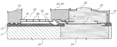
As illustrated with approximately 3000x magnification in Figure 1 and other
relevant drawing figures, a single inkjet nozzle device is shown as a portion
of a chip that is
fabricated by integrating MEMS and CMOS technologies. The complete nozzle
device
includes a support structure having a silicon substrate 20, a metal oxide
semiconductor
layer 21, a passivation layer 22, and a non-corrosive dielectric
coating/chamber-defining
layer 23.
The nozzle device incorporates an ink chamber 24 which is connected to a
source
(not shown) of ink and, located above the chamber, a nozzle chamber 25. A
nozzle opening
26 is provided in the chamber-defining layer 23 to permit displacement of ink
droplets
toward paper or other medium (not shown) onto which ink is to be deposited. A
paddle 27
is located between the two chambers 24 and 25 and, when in its quiescent
position, as
CA 02414734 2002-12-30
WO 01/02180 PCT/AU00/00586
-5-
indicated in Figures 1 and 7, the paddle 27 effectively divides the two
chambers 24 and 25.
The paddle 27 is coupled to an actuating arm 28 by a paddle extension 29 and a
bridging portion 30 of the dielectric coating 23.
The actuating arm 28 is formed (i.e. deposited during fabrication of the
device) to
be pivotable with respect to the support structure or substrate 20. That is,
the actuating arm
has a first end that is coupled to the support structure and a second end 38
that is movable
outwardly with respect to the support structure. The actuating arm 28
comprises outer and
inner arm portions 31 and 32. The outer arm portion 31 is illustrated in
detail and in
isolation from other components of the nozzle device in the perspective view
shown in
Figure 3. The inner arm portion 32 is illustrated in a similar way in Figure
4. The complete
actuating arm 28 is illustrated in perspective in Figure 5, as well as in
Figures 1, 7, 8, 9 and
10.
The inner portion 32 of the actuating arm 28 is formed from a titanium-
aluminium-
nitride (TiAI)N deposit during formation of the nozzle device and it is
connected
electrically to a current source 33, as illustrated schematically in Figure
11, within the
CMOS structure. The electrical connection is made to end terminals 34 and 35,
and
application of a pulsed excitation (drive) voltage to the terminals results in
pulsed current
flow through the inner portion only of the actuating arm 28. The current flow
causes rapid
resistance heating within the inner portion 32 of the actuating arm and
consequential
momentary elongation of that portion of the arm.
The outer arm portion 31 of the actuating arm 28 is mechanically coupled to
but
electrically isolated from the inner arm portion 32 by posts 36. No current-
induced heating
occurs within the outer arm portion 31 and, as a consequence, voltage induced
current flow
through the inner arm portion 32 causes momentary bending of the complete
actuating arm
28 in the manner indicated in Figures 8, 9 and 10 of the drawings. This
bending of the
actuating arm 28 is equivalent to pivotal movement of the arm with respect to
the substrate
20 and it results in displacement of the paddle 27 within the chambers 24 and
25.
An integrated movement sensor is provided within the device in order to
determine
the degree or rate of pivotal movement of the actuating arm 28 and in order to
permit fault
detection in the device.
The movement sensor comprises a moving contact element 37 that is formed
integrally with the inner portion 32 of the actuating arm 28 and which is
electrically active
when current is passing through the inner portion of the actuating arm. The
moving contact
element 37 is positioned adjacent the second end 38 of the actuating arm and,
thus, with a
voltage V applied to the end terminals 34 and 35, the moving contact element
will be at a
potential of approximately V/2. The movement sensor also comprises a fixed
contact
element 39 which is formed integrally with the CMOS layer 22 and which is
positioned to
CA 02414734 2002-12-30
WO 01/02180 PCT/AUOO/00586
-6-
be contacted by the moving contact element 37 when the actuating arm 28 pivots
upwardly
to a predetermined extent. The fixed contact element is connected electrically
to amplifier
elements 40 and to a microprocessor arrangement 41, both of which are shown in
Figure 11
and the component elements of which are embodied within the CMOS layer 22 of
the
device.
When the actuator arm 28 and, hence, the paddle 27 are in the quiescent
position, as
shown in Figures 1 and 7, no contact is made between the moving and fixed
contact
elements 37 and 39. At the other extreme, when excess movement of the actuator
arm and
the paddle occurs, as indicated in Figures 8 and 9, contact is made between
the moving and
fixed contact elements 37 and 39. When the actuator arm 28 and the paddle 27
are actuated
to a normal extent sufficient to expel ink from the nozzle, no contact is made
between the
moving and fixed contact elements. That is, with normal ejection of the ink
from the
chamber 25, the actuator arm 28 and the paddle 27 are moved to a position
partway
between the positions that are illustrated in Figures 7 and 8. This
(intermediate) position is
indicated in Figure 10, although as a consequence of a blocked nozzle rather
than during
normal ejection of ink from the nozzle.
Figure 12 shows an excitation-time diagram that is applicable to effecting
actuation
of the actuator arm 28 and the paddle 27 from a quiescent to a lower-than-
normal ink
ejecting position. The displacement of the paddle 27 resulting from the
excitation of Figure
12 is indicated by the lower graph 42 in Figure 14, and it can be seen that
the maximum
extent of displacement is less than the optimum level that is shown by the
displacement line
43.
Figure 13 shows an expanded excitation-time diagram that is applicable to
effecting
actuation of the actuator arm 28 and the paddle 27 to an excessive extent,
such as is
indicated in Figures 8 and 9. The displacement of the paddle 27 resulting from
the
excitation of Figure 13 is indicated by the upper graph 44 in Figure 14, from
which it can
be seen that the maximum displacement level is greater than the optimum level
indicated by
the displacement line 43.
Figures 15, 16 and 17 shows plots of excitation voltage, actuator arm
temperature
and paddle deflection against time for successively increasing durations of
excitation
applied to the actuating arm 28. These plots have relevance to fault detection
in the nozzle
device.
When detecting for a fault condition in the nozzle device or in each device in
an
array of the nozzle devices, a series of current pulses of successively
increasing duration tp
are induced to flow that the actuating arm 28 over a time period t. The
duration tp is
controlled to increase in the manner indicated graphically in Figure 15.
Each current pulse induces momentary heating in the actuating arm and a
CA 02414734 2002-12-30
WO 01/02180 PCT/AUOO/00586
-7-
consequential temperature rise, followed by a temperature drop on expiration
of the pulse
duration. As indicated in Figure 16, the temperature rises to successively
higher levels with
the increasing pulse durations as shown in Figure 15.
As a result, as indicated in Figure 17, under normal circumstances the
actuator arm
28 will move (i.e. pivot) to successively increasing degrees, some of which
will be below
that required to cause contact to be made between the moving and fixed contact
elements
37 and 39 and others of which will be above that required to cause contact to
be made
between the moving and fixed contact elements. This is indicated by the "test
level" line
shown in Figure 17. However, if a blockage occurs in a nozzle device, as
indicated in
Figure 10, the paddle 27 and, as a consequence, the actuator arm 28 will be
restrained from
moving to the normal full extent that would be required to eject ink from the
nozzle. As a
consequence, the normal full actuator arm movement will not occur and contact
will not be
made between the moving and fixed contact elements 37 and 39.
If such contact is not made with passage of current pulses of the
predetermined
duration tp through the actuating arm, it might be concluded that a blockage
has occurred
within the nozzle device. This might then be remedied by passing a further
current pulse
through the actuating arm 28, with the further pulse having an energy level
significantly
greater than that which would normally be passed through the actuating arm. If
this serves
to remove the blockage ink ejection as indicated in Figure 9 will occur.
As an alternative, more simple, procedure toward fault detection, a single
current
pulse as indicated in Figure 12 may be induced to flow through the actuator
arm and
detection be made simply for sufficient movement of the actuating arm to cause
contact to
be made between the fixed and moving contact elements.
Variations and modifications may be made in respect of the device as described
above as a preferred embodiment of the invention without departing from the
scope of the
appended claims.