Note: Descriptions are shown in the official language in which they were submitted.
CA 02414746 2003-01-03
Security paper and document of value produced therefrom
This invention relates to a security paper for producing documents of value,
such as bank notes, certificates, etc., with at least one multilayer security
element
having at least one visually checkable optical effect, the security element
being dis-
posed at least partly on the surface of the security paper. The invention
further relates
to a multilayer security element and to a document of value with such a
security ele-
ment. A transfer material for applying a multilayer security element to a
document of
value and a method for producing the transfer material and the document of
value are
also the subject matter of the invention.
There is a constant interest in protecting papers of value against forgery and
un-
authorized reproduction. It is becoming ever more difficult, particularly in
view of
today's copying and printing techniques, to find effective security features
that at least
make unauthorized reproduction or forgery clearly recognizable, if they do not
actu-
ally prevent it.
EP 0 019 191 B 1 proposes for example providing a paper of value with an inte-
grated circuit in which a checkable coding is written, the communication with
the
integrated circuit preferably being effected contactlessly via antennas. The
integrated
circuit is set in the gap of an at least partly metalized carrier foil. This
foil is then
laminated between two paper webs. Since the carrier foil is only laminated in
be-
tween the two paper webs, however, there is the danger that the layers can be
sepa-
rated from each other relatively easily so that the plastic inlay provided
with the chip
can be used for possible forgeries. Further, this security element is a
strictly machine-
checkable security element that can only be checked by means of special
detectors.
Frequently used authenticity features that are very easily visually checked
and
very striking are optically variable security elements, for example holograms,
that
show different visual impressions, such as color effects or information, from
different
viewing angles. A paper of value with such a security element is known from EP
0
440 045 A2. A bank note is described here that is provided with a label-like
holo-
gram. Since the optically variable effect of the hologram cannot be rendered
by a
CA 02414746 2003-01-03
-2-
color copier, these security elements offer very good protection against color
copy-
ing. However, these security elements have the disadvantage that they are very
poorly
checkable by machine, since the radiation reflected by the diffraction
structures of the
hologram must be detected at certain solid angles and the influence of stray
radiation
largely excluded to permit reliable ascertainment of the presence of a certain
holo-
gram. A further problem is the fluctuating signal intensity, since the latter
is greatly
dependent on the illumination source of the hologram. For reliable
measurement, de-
fined lighting conditions must therefore be ensured.
To avoid this problem, it was therefore also proposed to superimpose a
visually
readily visible hologram with a strictly machine-readable laser transmission
hologram
(DE 38 40 037 C2). Readout of the machine-readable hologram can be effected
only
by means of a laser, the information hidden in this laser transmission
hologram being
projected onto a certain space coordinate in front of the document of value
that is al-
ready defined when the hologram is recorded. The detector must be located at
this
place to permit this hidden information to be recognized. However, this type
of visual
and machine protection for a document of value is very elaborate both to
produce and
to check.
The invention is therefore based on the problem of proposing a document of
value and a security paper with a security element having a visually checkable
optical
effect and also being checkable by machine, the security paper and document of
value
being preferably easy and cost-effective to produce.
This problem is solved by the features of the independent claims. Developments
are the subject matter of the subclaims.
According to the invention, "security paper" designates the unprinted paper
that
can have not only the inventive security element but also further authenticity
features,
such as luminescent substances provided in the volume, a security thread or
the like.
It is usually present in quasi endless form and is processed further at a
later time.
CA 02414746 2003-01-03
-3-
"Document of value" refers to a document that is finished for its intended
use. It
may be for example a printed paper of value, such as a bank note, certificate
or the
like, an ID card, a passport or another document requiring protection.
The invention will be described hereinafter with reference to the security
paper.
However, the advantages and embodiments apply analogously to documents of
value.
According to the invention, the security paper is provided with at least one
mul-
tilayer security element having an optical effect that can be easily checked
visually
and not rendered by copying technology, or only in falsified form. This
security ele-
ment is disposed at least partly on the surface of the security paper and
contains at
least one integrated circuit in one of its inside layers. This integrated
circuit is for ex-
ample a strict memory chip (ROM), a rewritable chip (EPROM, EEPROM) or a mi-
croprocessor chip. The chips used have a thickness of 5 microns to 50 microns,
pref-
erably 10 microns, and an edge length of about 0.1 millimeters to 3
millimeters, pref-
erably 0.6 millimeters. On the chip there are preferably two to four contact
surfaces.
The optical effect of the security element can be produced by a layer
containing
optically variable pigments, in particular interference-layer or liquid-
crystal pigments.
This layer can be present all over or in the form of information.
Alternatively, the
security element can also have a hologram, kinegram or other diffraction
structure.
Preferably, the diffraction structures are embossed into a plastic layer in
the form of a
relief structure. If the diffraction structures are to be observable in
reflected light,
they are combined with a reflecting layer, in particular a metal layer or a
dielectric
layer with a high refractive index. The reflecting layer need not be provided
all over,
however, but can be applied in the form of a screen or any other information.
In par-
ticular, it can have gaps in the form of patterns or characters. A further
possibility for
producing a visually checkable optical effect is to use thin-film structures
wherein
metallic and/or dielectric layers with different refractive indexes are
disposed one
above the other, the layers cooperating so that different visual impressions
arise at
different viewing angles at least when viewed in reflected light. These
different visual
impressions are preferably different color effects.
CA 02414746 2003-01-03
-4-
Alternatively, the optical effect can also be produced by any printed image or
a
metallic layer with gaps in the form of patterns, characters or the like. The
metal layer
itself can likewise be present in the form of characters or patterns. The use
of special
printing inks, such as luminescent inks, is also possible. Of course, a
plurality of se-
curity features producing an optical effect can also be used. When a layer
producing
an optical effect is spoken of below, this also refers to cooperating
multilayer struc-
tures, such as the abovementioned dielectric thin-film elements or
combinations of a
plurality of layers that produce different optical effects. The term
"hologram" is like-
wise intended to stand for any diffraction structures.
The inventive integrated circuit is preferably disposed between this layer
having
the optical effect and the security paper. It is thus protected outwardly from
environ-
mental influences and practically does not appear visually. It is advantageous
to use
integrated circuits with which communication is effected contactlessly via a
coupling
element. The coupling element can already be an integrated part of the
integrated cir-
cuit or be disposed in a layer of the security element. Integration of the
coupling ele-
ment into the layer structure of the security element involves the advantage
that in
case of attempted manipulation or forgery the circuit cannot be separated
operably
from an original security element or a security paper equipped therewith, for
example
to be incorporated into a counterfeit reproduction. The coupling element can
be a
folded dipole, a coil or an open dipole. To increase the effectiveness of the
system,
the folded dipole or the coil can also have a metalized core zone. If the
coupling ele-
ment is formed on the layer producing the optical effect, the filled core zone
also
causes the visual impression of the layer to be less disturbingly influenced
by the
coupling element. The read range is between about 0.1 millimeters and a few
centi-
meters depending on the type of coupling element and the selected read/write
fre-
quency, for example 13.56 megahertz and 2 gigahertz.
The inventive security element is preferably applied to the security paper
after
papennaking and is so connected with the security paper that it cannot be
removed
without destroying the security paper or the security element. The invention
thus has
CA 02414746 2003-01-03
-5-
the advantage that the security element does not have to be integrated into
the paper-
making process and is nevertheless connected with the paper of value in
forgery-
proof fashion. A further advantage is that the security element is protected
against
attempts at forgery in several respects. The optical effect of the layers
facing the
viewer cannot be rendered true to the original with copying machines or other
repro-
duction techniques, so that such attempts at forgery can already be visually
recog-
nized easily and fast. If an attempt to reproduce or imitate the optical
impression of
the security element should succeed, however, the forgery can nevertheless be
recog-
nized upon the machine check of the integrated circuit. Since the circuit is
disposed
inside the security element and covered by the layers producing the optical
effect, a
potential forger will not notice this additional authenticity feature and
therefore not
attempt to imitate it.
The inventive security element is preferably formed as a multilayer self-
support-
ing label or as a transfer element that is connected with the security paper
after its
production. The contour form of the security element is freely selectable.
Alterna-
tively, the security element can also be formed as a security thread. In this
case, the
integrated circuit and the layer producing the optical effect are disposed on
a thread-
shaped plastic substrate that is so incorporated into the paper web during
papermak-
ing that the thread passes directly to the surface of the security paper in
partial areas.
According to a preferred embodiment, the security thread consists of two
plastic sub-
strates between which the integrated circuit and the layer producing the
optical effect
are disposed.
A "transfer element" refers according to the invention to a security element
that
is prepared on a separate carrier layer, for example a plastic foil, in the
reverse order
as it later comes to lie on the security paper, and then transferred to the
security paper
by means of an adhesive or lacquer layer in the desired contour forms. The
carrier
layer can be removed from the layer structure of the security element after
transfer, or
remain a firm part of the security element on the layer structure as a
protective layer.
CA 02414746 2003-01-03
-6-
The individual transfer elements can be prepared on the carrier layer as
separate
individual elements in the contour forms to be transferred. Alternatively, the
layer
sequence of the transfer elements is provided on the carrier layer in
continuous form.
Such carrier layers with spaced-apart individual transfer elements or a
continuously
extending layer structure will hereinafter be referred to as "transfer
material," and the
layer sequence of the security element disposed on the carrier layer as the
"transfer
layer."
In the case of the continuous transfer layer, the transfer material is then
con-
nected with the security paper via an adhesive layer, and the adhesive layer
activated
via suitable embossing tools so that the transfer layer adheres to the
security paper
only in the activated areas. All other areas are then removed with the carrier
layer.
Alternatively, the adhesive layer can also be executed in the form of the
security ele-
ment to be transferred. Adhesives preferably used are hot-melt adhesives.
However,
any other adhesives, such as reaction lacquers, can also be used.
The security element can alternatively be applied to the document of value.
The
embodiments and fastening possibilities described in connection with the
security
paper apply analogously in this case.
Hereinafter, some preferred layer sequences of the inventive security element
will be explained in more detail by the example of the transfer material.
The analogous layer sequence, only in the accordingly reverse order of layers,
can of course also be used for labels and security threads.
In the simplest form, the transfer material consists of a carrier layer, in
particu-
lar a transparent plastic foil, at least one layer producing the optical
effect and at least
one integrated circuit. In this embodiment the integrated circuit also
contains the cou-
pling element for communication with a readlwrite device.
If an integrated circuit not having an integrated coupling element is used, a
suit-
able coupling element must be provided in the layer structure of the transfer
layer of
CA 02414746 2003-01-03
-7-
the transfer material. The transfer layer with the integrated coupling element
is then
preferably formed as a thin, non-self-supporting foil. This thwarts attempts
at forgery
that aim at detaching the original security element from a security paper,
since the
non-self-supporting security element is not removable without being damaged.
This coupling element can be an open dipole, a folded dipole or a coil. This
cou-
pling element is preferably produced by suitable demetalizings in a metal
layer. For
this purpose the carrier layer of the transfer material, which is optionally
provided
with a separation layer, is provided with the layer producing the optical
effect. On
this layer a water-soluble or other layer soluble by means of a solvent is
then printed
in the form of the areas to be demetalized. In the next step, the carrier
layer is metal-
ized completely on the printed side. In a last step, the soluble ink and the
metalization
present in these areas are removed. The integrated circuit is fastened to this
layer by
means of a conductive adhesive layer, for example conductive silver or an
anisotropic
conductive adhesive. Finally, the carrier layer is provided with an adhesive
layer at
least in certain areas.
Alternatively, the structuring of the metal layer can also be effected by
means of
known etching techniques. In this connection, the carrier layer is provided
directly
with the all-over metalization after application of the layer producing the
optical ef-
fect. The metal layer is then printed with a protective lacquer layer in the
form of the
desired coupling element. The non-covered areas are then removed with suitable
sol-
vents. The protective layer can also be produced by photographic means by
coating
the metal layer all over with a photoresist that is then exposed and
developed.
According to a variant, the metallic layer forming the coupling element can be
separated from the layer producing the optical effect by an insulating layer.
This is
necessary in particular when the layer producing the optical effect likewise
has a con-
ductive layer.
According to a further embodiment of the invention, however, it is also
possible
that the metallic layer is at the same time required for the visually optical
effect. If a
CA 02414746 2003-01-03
-8-
reflection hologram is used for example, the layer producing the optical
effect usually
consists of an embossed lacquer layer in which the diffraction structures of
the holo-
gram are embossed in the form of a relief structure, and a metal layer. The
carrier
layer of the transfer material is first provided with the embossed lacquer
layer in
which the diffraction structures are embossed. This lacquer layer is then
provided
with a metal layer. Before the metal layer is preferably vapor-deposited,
however, a
soluble ink is printed on for producing the coupling element, as explained
above. Af-
ter metalization, the soluble ink is removed and the integrated circuit
applied, as
likewise described above. Here, too, the abovementioned etching techniques can
al-
ternatively be used for structuring the metal layer.
In this embodiment, the coupling element is to be recognized visually if the
em-
bossed lacquer layer, which forms the outermost layer facing the viewer in the
fin-
ished security element, is transparent. If this effect is undesirable, the
embossed lac-
quer layer can be colored. Preferably, metallic pigments are used for this
purpose.
Alternatively, the security element or security paper is laminated with a foil
or pro-
vided with a print that hides the optical impression of the coupling element.
This variant has the additional advantage that the layers of the security
element
ensuring the optical effect are undetachably connected with the machine-
checkable
integrated circuit. Manipulations of the layers producing the optical effect
thus simul-
taneously influence the machine-readable module.
However, the coupling element need not necessarily consist of an accordingly
formed metal layer. It can also be formed by a conductive polymer layer that
is ac-
cordingly printed for example.
The connection between coupling element and chip is effected in all embodi-
ments either by electrically conductive connecting elements, such as
conductive ad-
hesives, tin-lead solder, etc., or contactlessly, e.g. capacitively.
CA 02414746 2003-01-03
-9-
To make sure that manipulation by punching out a circuit together with the cou-
pling element from a security element or a security paper provided therewith
is no-
ticed, the coupling element is preferably designed to cover a large area. The
resulting
punched holes would already be very striking visually even to a layman as of
an area
assumed by the coupling element of 20 square millimeters or more.
The security paper provided with the inventive security elements can then be
processed into any documents of value. If bank notes are produced from the
security
paper for example, the security paper is usually cut into sheets with a
plurality of cop-
ies that can then be processed in suitable printing machines. Each copy has at
least
one inventive security element. In a preferred embodiment, the security
element is
formed as a strip extending parallel to one of the edges of a copy. This has
the advan-
tage that the security element can be transferred to the security paper in a
continuous
process.
During printing, the area of the security element can also be overprinted at
least
partially, thereby further increasing the forgery-proofness of the document of
value,
in particular if a tactile steel intaglio print is used for overprinting.
However, the in-
ventive security paper can also be used for producing other documents of
value, such
as passports, shares, visas, ID cards, certificates, admission tickets,
accompanying
documents for transportation, security labels or checks, etc. The documents of
value
can in turn be fastened as antiforgery elements to any products, such as CDs,
per-
fumes, pharmaceutical products, packages of all types.
The forgery-proofness of the inventive document of value can be increased even
further by storing certain data relevant to the document of value in the
integrated cir-
cuit in checkable fashion. For example, the history of use of the document of
value
can be stored in the integrated circuit. With bank notes for example,
information
about their issue and further life can be stored, thus permitting a hitherto
hardly pos-
sible evaluation of the circulation behavior of the notes. It is equally
possible to store
information about fitness or unfitness for circulation of bank notes.
CA 02414746 2003-01-03
- 10-
Further, it is possible to mark or block documents of value for certain
applica-
tions. Such marking could open up especially advantageous possibilities in
dealing
with blackmailing money.
In a special embodiment, the integrated circuit of the security element can be
additionally equipped or connected with a photosensitive sensor that is
likewise con-
tained in the security paper or the security element and recognizes for
example inci-
dent light, heat, magnetism and other properties. The measured values of such
sensors
are transmitted to the integrated circuit and stored there. This makes it
possible for
example to record each copying operation of a document as incident light and
to store
the number of copying operations in the integrated circuit. This offers the
advantage
of making it possible to distinguish between legal and illegal copies. When a
legal
copy is made, the user is aware that there is a corresponding sensor in the
security
paper so that he can then erase the information about his legal duplication
using a
device available only to him. Illegal duplication is not erased, however. If a
check is
done before each copying operation of whether the corresponding memory of the
in-
tegrated circuit has an entry, further copies can be prevented. This procedure
is suit-
able in particular for documents that are usually stored sealed from light.
Alternatively, identification numbers of the individual copying machines can
also be stored in the integrated circuit. This opens up the possibility that
all machines
used for producing copies can be identified at a later time. This can be
useful when
tracing forgers. Finally, copying machines can also be equipped with
corresponding
readers that prevent a copying operation of the document of value when reading
a
corresponding marking from the integrated circuit.
The integrated circuit can further be used for storing a type of electronic
stamp
of an issuing authority. This is of advantage in particular with visas or
passports. For
this purpose it is expedient to provide each document of value with individual
infor-
mation. This may be simple random numbers or more complex information which
can include features peculiar to the document, such as special printing
tolerances,
CA 02414746 2003-01-03
-11-
transmission properties of the paper or the like. This information can further
be en-
coded cryptographically.
However, the integrated circuit can also be used for protecting the legible in-
formation applied to the document of value. For example, if identification
informa-
tion such as a number and an indication of the issuer is entered on a document
of
value, the corresponding information can also be stored in the integrated
circuit. Stor-
age of this information is preferably effected in encrypted form that can only
be iden-
tified with the matching counter key. Upon a check of the document of value,
the in-
formation contained in the integrated circuit is compared with the information
actu-
ally present legibly on the document.
If communication with the integrated circuit is effected contactlessly, the
han-
dling of such documents is relatively simple. They can then be used for
example to
perform a virtually complete check in connection with goods deliveries, border
cross-
ings and other operations by which flows of goods are handled together with
docu-
ments. The invention can be used for example to check smuggling operations.
If a microprocessor is used as an integrated circuit, information encrypted by
suitable cryptographic methods can moreover be produced in the integrated
circuit of
the security paper or document of value and transferred to a read/write
device. Any
other programs or multifunctional structures can also be used. Techniques
known
from data processing or from the field of smart-card technology can be used
here.
Further examples and advantages of the invention will be explained with refer-
ence to the figures. It is pointed out that the figures are only for
illustration and do not
show the invention true to scale.
Fig. 1 shows an inventive document of value,
Figs. 2 to 5 show different embodiments of the inventive transfer material in
cross section,
CA 02414746 2003-01-03
-12-
Figs. 6a) to 6e) show different examples of the inventive coupling element.
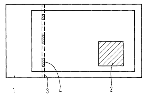
Fig. 1 shows a variant of the inventive document of value in a top view. The
ex-
ample shown involves bank note 1 produced from the inventive security paper.
The
bank note bears inventive security element 2 executed as a transfer element
and ap-
plied using the transfer material explained in more detail hereinafter. Bank
note 1 can
have additional security elements, for example security thread 3. Security
thread 3 is
quasi woven into the paper as a so-called "window security thread" so that it
passes to
the surface of the bank note in certain areas 4.
Figs. 2 to 5 show different embodiments of inventive transfer material 10.
Transfer material 10 consists fundamentally of carrier layer 5 and transfer
layer 6 that
is transferred to the inventive document of value at least in certain areas.
In the case
of security element 2 shown in Fig. 1, transfer layer 6 is detached from
carrier layer 5
in the form of a square for example. Carrier layer 5 can be provided with a
separation
layer to guarantee defined detachment of the transfer layer. This separation
layer is
not shown in the figures. Any other contour forms are of course also possible,
includ-
ing filigree structures such as guilloches, etc. Security elements 2
frequently also
have the form of strips disposed parallel to security thread 3.
Transfer layer 6 shown in Fig. 2 consists of layer 7 producing the optical
effect,
integrated circuit 8 and adhesive layer 9. Since integrated circuit 8 already
has an in-
tegrated coupling element, no further layers for communication with the
integrated
circuit are to be provided in the layer structure of transfer layer 6. Layer 7
producing
the optical effect is therefore freely selectable. However, it is preferably
opaque at
least in the area of integrated circuit 8 so that integrated circuit 8 is not
recognizable
visually.
Layer 7 producing the optical effect is shown all over here and can in turn be
composed of a plurality of layers. This is the case for example if it is a
thin-film ele-
ment, which can be composed of a plurality of dielectric layers with different
refrac-
CA 02414746 2003-01-03
-13-
tive indexes and thin metal layers. Such a layer structure produces an angle-
dependent interplay of colors.
Layer 7 can also be any other layer producing an optical effect, for example a
printed layer containing special pigments producing an optically variable
effect. For
this purpose liquid-crystal pigments or other pigments exploiting interference
effects
are preferably used, for example IRIODINE from the Merck company.
Adhesive layer 9 serves to fasten security element 2 to the document of value.
It
is preferably a hot-melt adhesive layer that is activated with the aid of
suitably
formed hot-stamping dies. However, adhesive layer 9 can also be provided only
in
certain areas to already define the contour form of the transfer elements to
be trans-
ferred on the transfer material. According to a further embodiment, it can
also be
completely absent. In this case the adhesive layer is applied in the desired
form to the
substrate that is to be provided with a transfer element.
The transfer material shown in Fig. 3 is provided with an integrated circuit
not
having an integrated coupling element. Transfer layer 6 therefore contains not
only
all-over layer 7 producing an optical effect but also metal layer 11. Metal
layer 11 is
applied in the form of a folded dipole, as shown in Fig. 6a), and forms the
coupling
element for integrated circuit 8. The connection between the terminals of
folded di-
pole 11 and the contact areas of the integrated circuit is effected via
conductive adhe-
sive layer 12.
Transfer layer 6 shown in Fig. 4 has a hologram consisting of embossed layer
13 and metal layer 14. Metal layer 14 ensures that the relief-like diffraction
structures
of the hologram can be observed in reflected light. However, metal layer 14
has
spaces 19. Spaces 19 are formed so as to result in coupling element 11 for
integrated
circuit 8. As in Fig. 3, the coupling element is formed by a folded dipole
insulated
from the rest of metal layer 14 by spaces 19.
CA 02414746 2003-01-03
-14-
In this example, metal layer 14 is simultaneously part of layer 7 producing
the
optical effect and of integrated circuit 8. However, coupling element 11 is to
be
clearly recognized in a top view if embossed layer 13 is of transparent
design. If this
effect is not desired, embossed layer 13 can be colored with translucent
colors. It is
also possible to use nonconductive, metallic-looking pigments that blur the
optical
impression of coupling element 12.
Transfer layer 6 shown in Fig. 5 likewise shows a hologram combined with an
integrated circuit. In the present case, reflecting layer 14 of the
diffraction structure
does not serve simultaneously as a communication layer for integrated circuit
8.
Rather, metal layer 14 is separated from metal layer 17 having coupling
element 11
by insulating layer 15. Nevertheless, metal layer 14 has gaps 16 in the form
of char-
acters or patterns that are well readable at least in transmitted light. These
gaps form a
further visual authenticity feature.
Metal layer 17 containing coupling element 11 is constructed analogously to re-
flecting layer 14 shown in Fig. 4. That is, it has spaces 19 that insulate
coupling ele-
ment 11 from the rest of the metal layer.
Gaps 16 and spaces 19 in metal layers 14 and 17 can be produced in different
ways. For example, the metal layers can be vapor-deposited by means of
correspond-
ing masks in the desired form directly on particular layer 13, 15.
Alternatively, the
metal layers can also be produced in a first step as all-over metal layers,
which are
then covered with a protective layer in the desired areas. The non-covered
free areas
are then removed with the aid of suitable solvents. These removed areas
correspond
to gaps 16 or spaces 19.
However, the method preferably used is to print layer 13, 15 in a first step
with
a preferably water-soluble ink in areas 16, 19. An all-over metalization is
then ap-
plied by vapor deposition. In a last step, the soluble ink and the metal layer
disposed
thereabove are removed with a corresponding solvent so that gaps 16 or spaces
19
CA 02414746 2003-01-03
- 15-
arise. It is likewise possible to produce gaps 16 using a different method
from that for
producing spaces 19.
The same methods can of course also be used for producing coupling element
11 as shown in Fig. 3.
Fig. 6 shows different embodiments of the coupling element. What is shown in
each case is solely the coupling element as used for example in Fig. 3. Any
further
metallic surroundings possibly present, as shown in Fig. 4 and 5, have been
omitted
for clarity's sake,.
Fig. 6a) shows a folded dipole, which can additionally be provided with a
metal-
lic core to increase the power of the system, as shown in Fig. 6b).
Alternatively, the
coupling element can also be executed as a coil with a corresponding number of
turns
or with a metallic core, as shown in Figs. 6c) and 6d). A further capacitively
operable
variant is shown in Fig. 6e). The two metallic bars act as an open dipole
here. These
forms of coupling elements can of course be used in all examples shown and de-
scribed.
As explained above, these coupling elements are preferably produced by a cor-
responding metalization or demetalizing. However, they can alternatively be
pro-
duced by printing technology with the aid of conductive polymers.
The layer structures of transfer material 10 shown in Figs. 2 to 5 can be
trans-
ferred analogously to a security thread. In this case, carrier layer 5 is
replaced with a
plastic foil undetachably connected with the layer structure disposed thereon.
The
layer structure here corresponds to transfer layers 6 shown. This security
thread can
be woven into the security paper analogously to security thread 3 shown in
Fig. 1.
However, the security thread can alternatively be disposed completely on the
surface
of the security paper or document of value. For this purpose the surface of
the plastic
carrier opposite the layer structure is coated with a suitable adhesive.
Analogously, it
CA 02414746 2003-01-03
-16-
is possible to produce the security element as a self-supporting adhesive
label with
any contour form.