Note: Descriptions are shown in the official language in which they were submitted.
CA 02414957 2002-12-20
ELECTROPHOTOGRAPHIC: PHOTOSENSITIVE MEMBER, PROCESS
CARTRIDGE AND ELECTROPHOTOGRAPHIC APPARATUS
BACKGROUND OF THE INVENTION
Field of the Invention
This invention relates to an electrophotographic
photosensitive member, a progress cartridge and an
electrophotographic apparatus. More particularly, it
relates to an electrophotographic photosensitive
member having on a conductive support at least a
charge generation layer, a charge transport layer and
a protective layer in this c>rder, and a process
cartridge arid an electrophotographic apparatus which
have such an electrophotographic photosensitive
member.
Related Background Art
In recent years, elect~rophotographic
photosensitive members are required to be made
further durable. For example, Japanese Patent
Application Laid-open No. ~~-173350 discloses that an
electrophotographic photosensitive member having very
good durability can be provided by forming on a
photosensitive layer a protective layer which
contains a curable resin. As another example,
Japanese Patent Application Laid-open No. 7-5748
discloses what is called injection charging, in which
electric charges are injected into a protective layer
CA 02414957 2002-12-20
- 2
on a photosensitive .Layer without being accompanied
with any substantial discharge.
However, while an ele,:trophotographic
photosensitive member having a protective layer has
the above-mentioned advantages, positive ghosts or
negative ghosts are liab7_e to occur. In addition,
such phenomena become conspi~~uous particularly in a
case where the protective layer contains a curable
resin as a binder resin.
On the other hand, with the recent development
of full-color photography or the minuteness realized
by dots as small as 1,200 dpi (dot per inch), much
higher image quality is demanded.
SUMMARY OF THE INVENTION
An object of the present invention is to
provide an electrophotographic photosensitive member
which hardly causes positive ghosts or negative
ghosts even in repeated use and can stably provide
high grade images.
In addition, other objects of the present
invention are to provide a process cartridge and an
electrophotographic apparatus having the
electrophotographic photosensitive member.
That is, the present invention provides an
electrophotographic photosensitive member comprising,
in this order, a photosensitive layer and a
CA 02414957 2002-12-20
_ 3 _.
protective layer on a conductive substrate, wherein
the surface of the electrophotographic photosensitive
member is charged to -?00 V and irradiated with white
light in a light quantity of 10 lux~sec under a 23
°C/5% RH environment., where Vsl(0.2), which is a
surface potential of: the e:le~~trophotographic
photosensitive member at the time 0.2 seconds have
passed from the irradiation, satisfies the following
formula (1) and the difference between the Vsl(0.2)
and Vsl(0.5), which is a surface potential of the
electrophotographic photosensitive member at the time
0.5 seconds have passed frorl the irradiation,
satisfies the following formula (2):
(V) C ~Vsl(0.2)~ ~ 80 (V) ... (1)
15 10 (V) ~ ~Vsl (0.2) - Vsl (0.5) ~ ~ 30 (V) . . . (2) .
The present invention further provides a process
cartridge and an electrophctographic apparatus having
the above electrophot.ographic photosensitive member.
20 BRIEF DESCRIPTION OF THE DRAWINGS
Figs. 1A, 1B and 1C are sectional views showing
examples of the layer construction of the
electrophotographic photosensitive member according
to the present invention.
Fig. 2 is a schematic view showing the
construction of Embodiment. 1 which is an
electrophotographic apparatus provided with a process
CA 02414957 2002-12-20
- 4
cartridge having the electrophotographic
photosensitive member accord~_ng to the present
invention.
Fig. 3 is a schematic view showing the
construction of Embodiment 2 which is another
electrophotographic apparatus provided with a process
cartridge having the electrophotographic
photosensitive member according to the present
invention.
Fig. 4 is a chart of CuKa characteristic X-ray
diffraction characteristic of hydroxygallium
phthalocyanine used in Examples of the present
invention.
DETAILED DESCRIPTION OF THE PREFERRED EMBODIMENTS
In the present invention, Vsl(0.2), which is a
surface potential of the electrophotographic
photosensitive member at the time 0.2 seconds have
passed after the ~~urface of the e7_ectrophotographic
photosensitive rr~ember is charged too -700 V and
irradiated with white light in a Light quantity of 10
lux~sec under a 23 °C/5o F;H environment, satisfies
the following formula (1), and the difference between
the Vsl(0.2) and Vsl_(0.5),, which is a surface
potential of the electrophotographic photosensitive
member at the time 0.5 seconds have passed after the
irradiation with the white light, satisfies the
CA 02414957 2002-12-20
- 5 -
following formula (2):
20 (V) ~ ~Vs1(0.4)~ ~ 80 (v) ... (1)
(V) ~ ~Vsl (0.2~ -- ~Is:L (0.5) ~ < 30 (V) . . . (2) .
Embodiments of the pre:>ent invention will be
5 described below in detail.
As stated above, in the elects°ophotographic
photosensitive member havi.nc~ a protective layer,
there was such problems that_ positive ghosts or
negative ghosts were liable to occur, and blurred
10 images tended to occur under high temperature and
high humidity environment, with such phenomena
conspicuously appeari..ng particularly in a case where
the protective layer contains a curable resin as a
binder resin.
The present inventor: presumed that these
problems were ascribable to electric charges
accumulated at the interface formed between the
charge transport layer a.ncl the protective layer.
In recent years, research and development on
protective 1_ayer~~ of electrophotographic
photosensitive members is progressing at dizzy speed,
but there is no change in that the interface is
formed between the photosensitive layer and the
protective layer. Such a tendency is strong
especially where a curable resin is used in the
protective layer.
Charges generated in the photosensitive layer
CA 02414957 2002-12-20
- 6 -
move through the photosensitive layer to reach the
above interface and enter t:he protective layer, but
some charges are supposed usually to accumulate at
the interface. The present inventcrs presumed that
the above positive and negative ghosts would be
caused by the ~.~harge accumulation at the interface.
That is, in the case of an electrophotographic
photosensitive member having a protective layer,
charges having moved through the photosensitive layer
after exposure reach the interface between the
photosensitive layer and the protective layer to be
accumulated, or stay in the protective layer. In
such a place, when the seccnd round charging is
conducted, the absolute value of the surface
potential is reduced by the influence of the
accumulated or stayed charges, appearing as positive
ghosts when half-tone images are reverse-developed.
On the other hand, if the above accumulated or
stayed charges are further remarkable, a lot of
charges are left. acc:umulat.ed or stayed even when the
second round charging is carried out, and due to the
influence of the previously accumulated or stayed
charges together with the influence of charge
accumulation and stay newly caused by exposure for
forming half-tone images, the absolute value of the
surface potential is not sufficiently reduced,
appearing as negative ghosts when half-tone images
CA 02414957 2002-12-20
-
are reverse-developed.
Therefore, the present inventors found that the
above-described technical subject can be solved by
delicately controlling the above accumulated or
stayed charges, specifically by regulating the
potential characteristics of the 1ec trophotographic
photosensitive member so that the conditions
represented by the abc>ve formulas (1) and (2) are
satisfied and arrived at the present invention. The
present inventors have performed various studies from
the above viewpoints, arid based on their experience,
derived the above formulas (1) and (2) in the present
invention.
The characteristics of the electrophotographic
photosensitive member according to the present
invention is defined by t:he surface potential of the
electrophotographic photosensitive member after
charging the surface of the electrophotographic
photosensitive member to -700 V and irradiating the
charged surface with white light in the light
quantity of 10 lux~sec.
In the present invention, the residual
potential ~Vsl(0.2)~ at the time ().2 seconds have
passed after.' the irradiation with the white light is
20 V or more and 80 V or less, preferably 20 V or
more and 70 V or less, and particularly 20 V or more
and 60 V or less. If the ~Vsl(0.2)~ is less than 20 V,
CA 02414957 2002-12-20
_.
positive ghosts are liable to occur, and if the
~Vsl(0.2)~ is more than 80 V, negative ghosts are
liable to occur.
However, it is not sufficient to define only
the range of the ~ Vsl ( () . 2 ) ~ , and in the present
invention it is further necessary that the difference
between the Vs.l(0.2) and the residual potential
Vsl(0.5) at the time 0.5 seconds have passed after
the irradiation with the white light (~Vsl(0.2) -
Vsl(0.5)~) is 10 V or more and 30 V or less. If the
~Vsl(0.2) - Vsl(0.5)~ is less than 10 V, the
attenuation in a short time of the potential is too
small, i.e., charges are liable to accumulate or stay,
and in the case of reverse deve:Lopment, negative
ghosts would occur. On the other viand, if the
~Vsl(0.2) - Vsl(0.5)~ is more than 30 V, the
attenuation in a short time of the potential is too
large, i.e., the a.bsolutE: value of the surface
potential at the time of the second charging becomes
too low, resulting in positive ghosts. In the
present invention, the ~ Vs_L ( 0 . 2 ) - Vs 1 ( 0 . 5 ) ~ i s
preferably 12 V or more and 25 V or less.
These surface potentials were measured under
the 23 °C/5° RH envi.ronment. By evaluating the state
of the accumulation or sta y of charges under such a
low humidity, more substantial electrophotographic
characteristics can be evaluated.
CA 02414957 2002-12-20
- 9
From the interface viewpoint, the constitution
of the protective layer is cited as a factor having a
great influence on the afore-mentioned potential
characteristics. Such a constitution of the
protective layer includes ki:ads of compounds
contained in therein, the composition rate thereof,
the cross-liking degree of a binder resin, the
thickness thereof, and types and mixing ratio of
compounds contained in the photosensitive member, but
in the present invention, it. is important that the
electrophotographic photosensitive member has the
afore-mentioned potential characteristics and
measures for realizing such characteristics is not
particularly limited.
However, there are preferred embodiments for
realizing the above potential characteristics, hence
the constitution thereof is described below in detail.
The protective layer of the electrophotographic
photosensitive member according to the present
invention may preferably b~~ a layer containing a
binder resin and at lea st one of conductive particles
and a charge-transporting materia;L.
As the binder resin for the protective layer,
curable resins are preferred. In particular,
phenolic resins, epoxy resins and siloxane resins are
more preferred. Still in particular, phenolic resins
are preferred because the electrical resistance of
CA 02414957 2002-12-20
the protective layer may less> undergo environmental
variations. Then, particularly more preferred are
heat-curable resol type phenolic resins in view of
advantages that they can provide a high surface
hardness, promise superior wear resistance and also
afford superior dispersibility for fine particles and
superior stabi:Lity after their dispersion.
Curable phenolic resins are resin obtained
commonly by the reaction of phenolics with
formaldehyde.
The phenolic resins have two 'types, and are
divided into a resol type obtained by the reaction of
a phenolic with formaldehyde, the latter being used
in excess in respect to the former, in the presence
of an alkali catalyst, and a novolak type obtained by
the reaction of a phenolic with formaldehyde, the
former being used in exces:> in respect to the latter,
in the presence of an acid catalyst.
The resol type is soluble in alcohol type
solvents and also in ke tone type solvents. It
undergoes three-dimensionally cross-linking
polymerization upon heating, and comes into a cured
product. As for the novolak type, it usually does
not cure when heated as it is, but forms a cured
product upon heating with addition of a formaldehyde
source such as paraformaldehyde cr
hexamethylenetetramine.
CA 02414957 2002-12-20
- 11 -
Commonly and industrially, the resol type is
utilized in coating material's, adhesives, castings
and laminating varnishes. The novolak type is
chiefly utilized in molding materials and binders.
In the present invention, either of the resol
type and the novolak type may be used as the phenolic
resins. In view of the ability t.o cure without
addition of any curing agent and the operability as
coating materials, it is preferable to use the resol
type.
Where the phenolic resins are used in the
present invention, any of phenolic resins may be used
alone or in the form of a mixture of two or more. It
is also possible to use the resol type and the
novolak type in cornbination. Also, any known
phenolic resins may be used.
Resol type phenolic resins ar_e usually produced
by reacting phenolic compounds with aldehyde
compounds in the presence of an alkali catalyst.
Chief phenolic compounds to be used may include,
but are not limited to, phenol, cresol, xylenol,
para-alkylphenols, para-phenylphenol, resorcin and
bisphenols. The aldehyde compounds may also include,
but are not limited to, fc~rmaldehyde,
paraformaldehyde, furfural and acetaldehyde.
These pheno:lic compounds and aldehyde compounds
may be allowed to react in the presence of an alkali
CA 02414957 2002-12-20
1-~ _
catalyst to produce any of monomers of
monomethylolphenols, dimethy~.olphenols or
trimethylolphenols, mixtures of these, or those
obtained by making them into oligomers, and mixtures
of these monomers arid oligomers. Of these,
relatively large mo7_ec:ules having about 2 to 20
repeating units of molecular structure are the
oligomers, and those having a single unit are the
monomers.
The alkali catalyst to be used may include
metal type alkali compounds and amine compounds. The
metal type alkali compounds may include, but are not
limited to, alkali metal or alkaline earth metal
hydroxides such as sodium hydroxide, potassium
hydroxide and calcium hydroxide. The amine compounds
may include, but are not limited to, ammonia,
hexamethylenetetramine, trimethylamine, triethylamine
and triethanolami.ne.
In the present invention, taking account of
variations of electrical resistance in an environment
of high humidity, amine compounds may preferably be
used, and, taking account of other
electrophotographic performances, may also be used in
the form of a mixture with any of the metal type
alkali compounds.
The protective layer of t:he electrophotographic
photosensitive member according to the present
CA 02414957 2002-12-20
- 13
invention may preferab7_y be formed by coating on the
photosensitive layer a coating solution prepared by
dissolving the curable phenolic resin in, or diluting
it with, a solvent or the liJ~e, whereby
polymerization reaction takes place after coating and
a cured layer is formed. The polymerization proceeds
by addition and condensation reaction caused by
heating, where the protective layer is formed by
coating, followed by heating to cause polymerization
reaction to take place to form a polymeric cured
layer in which the resin has cured.
In the present invention, what is meant by "the
resin has cured" is that the resin stands insoluble
even when wetted with an alcohol solvent such as
methanol or ethano'.
The conductive partic=Les for the protective
layer have an auxiliary function to control the
volume resistivit.y of' the ~>rotective layer, and need
not necessarily be used if unnecessary.
The conductive particles usable in the
protective layer of the electrophotographic
photosensitive member according to the present
invention may include metal particles and metal oxide
particles.
The metal particles may include aluminum, zinc,
copper, chromium, nickel, silver and stainless steel
particles, or particles of: plastic on the surfaces of
CA 02414957 2002-12-20
_ 1q _
which any of these metals hay; been vacuum-deposited.
The metal oxide particles may include zinc oxide,
titanium oxide, tin oxide, antimony oxide, indium
oxide, bismuth oxide, tin-doped indium oxide,
antimony- or tantalum-doped 'tin oxide, and
antimony-doped zirconium oxide particles.
Any of these may be used alone or may be used
in combination of two or more types. When used in
combination of two or more types, they may merely be
blended or may be made into a solid solution or a
fused solid.
In the present invention, among the conductive
particles described above, the use of metal oxides is
preferred in view of the transparency. Of these
metal oxides, the use of tin oxide is further
particularly preferred. Th~~ tire oxide may be, for
the purpose of improving dispersibility and liquid
stability, one having been subjected to surface
treatment described =Later, or may be, for the purpose
of improving resistance controllability, one having
been doped with antimony o:r tantalum.
The conductive particles for the protective
layer may preferably have an average particle
diameter of 0.3 ~.rn or less, and particularly 0.1 ~m
or less, from the viewpoint of transparency of the
protective layer. On the other_ hand, from the
viewpoint of dispersibil.it:y and dispersion stability,
CA 02414957 2002-12-20
_ 15 _
they may preferably have an average particle diameter
of 0.001 ~.tm or more.
From the viewpoint of film strength of the
protective layer, the protective layer comes weaker
with an increase in the quantity of the conductive
particles. Accordingly, the conductive particles may
preferably be in a small quantity as long as the
volume resistivity and residual potential of the
protective layer are tolerable.
The protective layer of the e=Lectrophotographic
photosensitive member according to the present
invention may also preferably be a layer containing
lubricating particles
The lubricating particles for the protective
layer may preferab:Ly include fluorine-atom-containing
resin particles, silicone resin particles, silica
particles and alumina particles, and more preferably
be fluorine-atom-containi.nc~ resin particles. Also,
two or more kinds of these may be blended.
The fluorine-atom-containing resin particles
may include particles of tetrafluoroethylene resin,
trifluorochlo roethylene resin, hexafluoroethylene
propylene resin, vinyl fluoride resin, vinylidene
fluoride resin, difluorodichloroethylene resin and
copolymers of these, any one or more of which may
preferably appropriately k>e selected.
Tetrafluoroethylene resin particles and vinylidene
CA 02414957 2002-12-20
- 1E~ --
fluoride resin particles are particularly preferred.
The molecular weight' and particle diameter of
the lubricating particles ma~,~ appropriately be
selected, without any particular limitations.
Preferably, they may have a rnolecular weight of from
3,000 to 5,000,000, and an a~aerage particle diameter
of from 0.01 ~.m to 10 ~.un, and more preferably from
0 . 0 5 ~.m t o 2 . 0 ~.m .
Inorganic particles such as silica particles
and alumina particles do not function as the
lubricating particles in themselves in some cases.
However, studies made by the present inventors have
revealed that by dispersing and adding those
particles, the protective layer have a larger surface
roughness, and consequently can have an improved
lubricity. In the present invention, the lubricating
particles are meant. to include part=isles capable of
providing lubricity.
When the conductive particles and the
lubricating particles such as
fluorine-atom-containing resin particles are
dispersed together i.n a resin solution, in order to
make these particles not undergo mutual agglomeration,
the fluorine-atom-containing compound may be added at
the time the conductive particles are dispersed, or
the conductive particles may be surface-treated with
the fluorine-containing compound.
CA 02414957 2002-12-20
._
Compared with a case in which any
fluorine-atom-containing compound is not added, the
addition of the fluorine-atom-containing compound to
the conductive particles or t:he surface treatment of
the latter with the former brings about a remarkable
improvement in dispersibility and dispersion
stability of the condu<~tive particles and
fluorine-atom-containing resin particles in the resin
solution.
The fluorine-atam-containing resin particles
may also be dispersed in a liquid d:i_spersion in which
the fluorine -atom-containing compound has been added
and the conductive particles have been dispersed, or
in a liquid dispersion in which the surface-treated
conductive particles have been dispersed. This
enables preparation of a protective-layer coating
fluid free of any formation of secondary particles of
dispersed particles, very stable: over time and having
a good dispersion.
The fluorine-atom-cont=aining compound may
include fluorine-containing sil.ane coupling agents,
fluorine-modified silicone oils and fluorine type
surface-active agents. Examples of preferred
compounds are given below. In the present invention,
examples are by no means limited to these compounds.
CA 02414957 2002-12-20
._
Examples of fluorine-containing silan~s coupling agents
CF~CH2CH~Si(OCH~)~
C4F~CH~CHZSi(OCH~3
CBFiaCH2CH~Si(C)CH~)3
CBF~yCH2CH2Si(OCH3)3
CBF~ 7CH2CHZSi(C?CH2CH20CH~)3
C~oF2~si(OCHa)3
C~F~3CONHSi(OCH3)3
C$F~7CONHSi(OCH3)~
C~Fi SCONHCH~CHZCH2Si(f3CH~)3
C~F15CONHCH2CH2CHzSi(~ZHS)3
C~F~SCOONHCH2CH~CH2,Si(OCH3)3
C7F~5COSNHCH2CH2CH~Si(OCH3)3
C~F~SSO~hiHCH~CH2CH2S1(OC2H5)3
C~FiTS021; CH2CH2CH~Si(OCH~)~
CH~CH2CH~
C,~Fi~CH2Ci-i2SCHaCH~Si(OGH3)a
Ct,~mCH~CH~SCH2CH~Si(OCH3)3
C~Ff~CtINHCH~CHzNCH2CH~CH2Si(OCH3)~
~~7F15
C~FigSO~NHCH2CH2NCH~CH~CH~Si~OCH~)3
SO!~C8F17
CA 02414957 2002-12-20
Fxa~les of fluoruie-rrr~dified silicone oils
H~ j R ~H3 CH3
H3C- ~i- O Si- O Si- O $i- CH3
'CH3 m ~ CH3 n ''Chip
R : -CHpCHgCF3 m and n : positive integers
CA 02414957 2002-12-20
Examples of fluorine type surface-active agents
x-sar'Zr~CHZeoaH
X-SCIiNHCH~CHZa(CHZCHZU) "H
X-S~JzN(CI-~aCHzC>E~30H)z
X-RiJ(CHzCHzO)"H
x.(~xo~n~~
x-~RO)a~z
X-SOxNRCH2 ~ % H.Z
d
X-CO~H ~ X-CIiiCH~CClOiI<
X-QKCUHH
X-ORCHZC4UH ~ X-StJ;H
X-ORSQ~H ? X-GHzC:Ha(II~I
X-CHZaCH2CHCHZ
O
X-CH~CH~OCHz \ ~ Hs
O
X-GUZGHz ~ ~ H2
O
R : alkyl group, aryl group or aralkyl group.
X : fluorocarbon group such as -CF3, -C~F8
or -CSF 1z
n 5, 1 Q or-15
CA 02414957 2002-12-20
- 21
As a method for the surface treatment of the
conductive particles, t:he conductive particles and
the surface-treating agent may be mixed and dispersed
in a suitable solvent too make the surface-treating
agent adhere to the conductive-particle surfaces.
They may be dispersed by using a usual dispersion
means such as a ball mill or a sand mill. Next, the
solvent may be removed from the resultant liquid
dispersion to fix the surface-treating agent to the
conductive-particle surfaces.
After this treatment, heat treatment may
further optionally be made. Also, yin the
surface-treating dispersion, a catalyst for
accelerating the reaction may be added. Still also,
the conductive particles hawing been surface-treated
may further optionally be subjected to pulverization.
The proportion of the fluorine-atom-containing
compound to the conductive particles is influenced by
the particle diameter, shape and surface area of the
particles to be treated, and the former may
preferably be in an amount of from 1 to 65°s by weight,
and more preferably from 1 to 50o by weight, based on
the total weight ef the conductive particles having
been surface-treated.
In the present invention, in order to provide a
protective layer having a higher environmental
stability, a siloxane compound having structure
CA 02414957 2002-12-20
represented by the following Formula (1) may further
be added at the time the conductive particles are
'dispersed, or conductive particles having been
surface-treated with the siloxane compound having
structure represented by the following Formula (1)
may further be mixed. This a nables the protective
layer having much higher environmental stability to
be formed.
A12 Am A1s
A11-Si C)-Si Ca-Si A1g ( 1 )
A13 A15 n1t '~17
In Formula i 1 ) , Al~ to A~$ are each independently
a hydrogen atom or a methyl group, provided that the
proportion of the total number (b) of the hydrogen
atoms in the total number (a) of A's, b/a, ranges
from 0.001 or more to 0.5 or less; and nll is an
integer of 0 or more.
This siloxane compound is added to the
conductive particles, followed by dispersion, or
conductive metal oxide particles surface-treated with
this siloxane compound is dispersed in a binder resin
dissolved in a so~.vent, thereby preparing a
protective-layer coating fluid free of secondary
particles of dispersed particles and more stable in
its dispertion over time. Also, t:he protective layer
CA 02414957 2002-12-20
- 23
formed using such a coating fluid can have a high
transparency, and a film having especially good
environmental resistance can be obtained.
There are no p<~rticular limitations on the
molecular weight of the siloxane compound having
structure represented by the above Formula (1).
However, when the conductive particles are
surface-treated with .it, it is better for the
compound not to have too high a viscosity in view of
the readiness of surface treatment. It may
preferably have a weight-average molecular weight of
from 100 to 50,000, and part=icularly preferably from
500 to 10,000 in view of the treatment efficiency of
the surface treatment.
As methods for the surface treatment, there are
two methods, a wet process ~~.nd a dry process.
In the wet-process t:re atment, the conductive
particles (conductive metal oxide particles) and the
siloxane compound having structure represented by
Formula (1) are dispersed in a sol~rent to make the
siloxane compound adhere to the particle surfaces.
As a dispersion means, they may be dispersed by
using a usual dispersion means such as a ball mill or
a sand mill. Next, this dispersion is made to fix to
the conductive-particle surfaces by heat treatment.
In this heat treatment, Si-H bonds in siloxane
undergo oxidation of hydrogen atoms which is caused
CA 02414957 2002-12-20
- 24 -
by the oxygen in air in the course of the heat
treatment to form additional siloxane linkages. As
the result, the siloxane comes to have a
three-dimensional network structure, and the
conductive-particle surfaces are covered with this
network structure. Thus, the surface treatment is
completed upon making the siloxane compound fix to
the conductive-particle surfaces, The particles
having been thus treated may optionally be subjected
to pulverization treatment.
In the dry-process treatment, the siloxane
compound and the conductive metal oxide particles are
mixed without use cf any so=went, followed by
kneading to make the sil_oxane compound adhere to the
particle surfaces. Thereafter, as i.n the case of the
wet-process treatment, the resultant particles may be
subjected to heat treatment and pulverization
treatment to complete the surface treatment.
As the charge-transporting material usable in
the protective layer of the electrophotographic
photosensitive member according to the present
invention, a compound having at least one hydroxyl
group in the molecule i_s preferred. In particular, a
compound having at least one hydroxyalkyl group,
hydroxyalkoxyl group or hydroxyphenyl group in the
molecule is preferred.
As a charge-transporting material having at
CA 02414957 2002-12-20
- 25 -
least one of a hydroxyalkyl group and a
hydroxyalkoxyl group in the molecule, a
charge-transporting material having the structure
represented by any of the f_o:Llowing Formulas (2) to
(4) is preferred.
HO R21 O ~ O-~--R2~-OH
lL
a
m N ~ (2)
HO R~ O I
.-
n
In Formula ( 2 ) , R~1, R'Z and R23 each
independently represent a divalent hydrocarbon group
having 1 to 8 carbon atoms and which may be branched.
The benzene rings ox, (3 and y may each independently
have as a substituent a halogen atom, a substituted
or unsubstituted alkyl group, a substituted or
unsubstituted alkoxy~ group, a substituted or
unsubstituted aromatic hydrocarbon ring group or a
substituted or unsubstituted aromatic heterocyclic
group. Letter symbols a, b, d, m and n each
independently represent 0 or 1.
CA 02414957 2002-12-20
- 26 -
HO R31 O ~ O-~--R.33_OH
O
a .
N ~ ~ r (3)
HO R32 O E ~ 31
3~
In Formula ( 3 ) , R31, R3' and R3'' each
independently represent a divalent hydrocarbon group
having 1 to 8 carbon atoms and which may be branched.
The benzene rings 8 and s may each independently have
as a substituent a halogen <atom, a substituted or
unsubstituted alkyl group, a substituted or
unsubstituted alkoxyl group, a substituted or
unsubstituted aromatic hydrocarbon ring group or a
substituted or unsubstituted aromatic heterocyclic
group. Letter symk>ols e, f and g each independently
represent 0 or 1. Letter symbols p, q and r each
independently represent. C1 or 1, provided that a case
in which all of them are simultaneously 0 is excluded.
Z31 and Z3z each independently represent a halogen
atom, a substituted or unsubstitut=ed alkyl group, a
substituted or unsubst:ituted alkoxyl group, a
substituted or un.substituted aromatic hydrocarbon
ring group or a substituted or unsubstituted aromatic
heterocyclic group, or ma~,~ combine to form a ring.
CA 02414957 2002-12-20
- 27 -
HO R41 O -OH
h
t
N
J
(4)
J
HO R~--~-O O-~-R44-OH
j k
a
In Formula ( 4 ) , R41, R''Z~ R43 and R44 each
independently represent a divalent hydrocarbon group
having 1 to 8 carbon atoms and which may be branched.
The benzene rings , r~, 8 and t may each independently
have as a substit;uent~ a halogen atom, a substituted
or unsubstituted alkyl group, a substituted or
unsubstituted alkoxyl group, a substituted or
unsubstituted aromatic hydrocarbon ring group or a
substituted or unsubstituted aromatic heterocyclic
group. Letter symbo:Ls hr :i, j, k, s, t and a each
independently represent 0 or 1. Z91 and Z42 each
independently represent a halogen atom, a substituted
or unsubstituted alkyl group, a substituted or
unsubstituted alkoxyl group, a substituted or
CA 02414957 2002-12-20
- 28 -
unsubstituted aromatic hydrocarbon ring group or a
substituted or unsubstituted aromatic heterocyclic
group, or may combine to form a ring.
As a charge-transporting material having a
hydroxyphenyl group in the molecule, a
charge-transporting material having structure
represented by any of the following Formulas (5) to
(7) is preferred.
UH
K
51
N Ar~3 O R~1 C R51 ( 5 )
v w
OH
In Formula (5), R51 represents a divalent
hydrocarbon group having 1 to 8 carbon atoms and
which may be branched. 152 represents a hydrogen atom,
a substituted or unsubstituted alkyl group, a
substituted or unsubstituted aralkyl group or a
substituted or unsubstituted phenyl group. Ar51 and
Ar52 each independently represent a substituted or
unsubstituted alkyl group, a substituted or
CA 02414957 2002-12-20
- 29 -
unsubstituted aralkyl croup, a substituted or
unsubstituted aromatic hydrocarbon ring group or a
substituted or unsubst.ituted aromatic heterocyclic
group. Ar53 represents a substituted or unsubstituted
divalent aromatic hydrocarbon ring group or a
substituted or unsubstituted divalent aromatic
heterocyclic group. Letter ;cymbals v and w each
independently represent 0 or 1, provided that w is 0
when v is 0. The benzene rings tc and ~, may each
independently have as a subs>tituent a halogen atom, a
substituted or unsubstituted alkyl group, a
substituted or unsubstituted alk.oxyl group, a
substituted or unsubstituted aromatic hydrocarbon
ring group or a substituted or unsubstituted aromatic
heterocyclic group.
~,61
>> OOH (s)
x,62 R61
x ~'
In Formula (6), R61 represents a divalent
hydrocarbon group having 1 to 8 carbon atoms and
which may be branched. ArE'1 and Ar_b2 each
independently represent a substituted or
unsubstituted alkyl group, a substituted or
unsubstituted aralkyl group, a substituted or
CA 02414957 2002-12-20
- 30 -
unsubstituted aromatic hydrocarbon ring group or a
substituted or unsubstituted aromatic heterocyclic
group. Letter symbol x represents 0 or 1. The
benzene rings p and v rnay each independently have as
a substituent a halogen atom, a substituted or
unsubstituted alkyl group, a substit=uted or
unsubstituted alkoxyl group, a substituted or
unsubstituted aromatic hydrocarbon ring group or a
substituted or unsubstitutec, aromatic heterocyclic
group, or the benzene ring's ~, and v may combine via a
substituent to form a ring.
N C
HO ~~ ~ ~ OH
Rm x,71 R7z
y z
In Formula ( ~' ) , R'1 and R7? each independently
represent a divalent hydrocarbon group having 1 to 8
carbon atoms and which may be branched. Ar'1
represents a substituted or unsub~tituted alkyl group,
a substituted or unsubstituted aralkyl group, a
substituted or unsubstituted aromatic hydrocarbon
ring group or a substituted or unsubstituted aromatic
heterocyclic group. Letter symbols y and z each
independently represent 0 or 1. The benzene rings ~,
~t, p and a may each independently have as a
substituent a halogen atom, a substituted or
CA 02414957 2002-12-20
- 31 -
unsubstituted alkyl group, a substituted or
unsubstituted alkoxyl group, a substituted or
unsubstituted aromatic hydrocarbon ring group or a
substituted or unsubstituted aromatic heterocyclic
S group. The benzene rings ~ and rt and the benzene
rings p and a rnay each independently combine via a
substituent to form a ring.
In the above formulas (2) to (7), the divalent
hydrocarbon groups represented by R11, RZ', R23, R31,
R32, R33r R41, R4Z, R43I R44, R51I R61/ R71 and R72, having
1 to 8 carbon atoms and which may be branched, may
include alkylene groups such as a methylene group, an
ethylene group, a propylene group and a butylene
group, an isopropy.Lene group, and a cyclohexylidene
group.
The alkyl group represented by R~2 may include a
methyl group, an ethyl group, a propyl group and a
butyl group; and the aralkyl group may include a
benzyl group, a phenethyl group and a naphthylmethyl
group.
Of the substituents the benzene rings a, (3, 'y, b,
T~, 8, 1, K, ~,, ~.1, V, ~, TC, p and 6 may have, the
halogen atom may include a. fluorine atom, a chlorine
atom, a bromine atom and an iodine atom; the alkyl
group may include a methyl_ group, an ethyl group, a
propyl group and a butyl group; the alkoxyl group may
include a methoxyl group, an ethoxyl group, a
CA 02414957 2002-12-20
- 32 -
propoxyl group and a butoxyl group: the aromatic
hydrocarbon ring group may include a phenyl group, a
naphthyl group, an anthryl group and a pyrenyl group:
and the aromatic heterocyclic group may include a
pyridyl group, a thienyl group, a furyl group and a
quinolyl group.
In the cases in which the benzene rings ~, and v,
the benzene rings ~ and ~ and the benzene rings p and
a each combine via a substituent to form a ring, the
substituent may include a propylidene group and an
ethylene group. Via such groups, <cyclic structures
such as a fluorene skeleton and a dihydrophenanthrene
skeleton are formed.
The halogen atoms represented by Z31, Z3~, z4i
and 242 may also include a fluorine atom, a chlorine
atom, a bromine atom and a.n iodine atom: the alkyl
group may include a methyl group, an ethyl group, a
propyl group and a butyl group; the alkoxyl group may
include a methoxyl group, an ethoxyl group, a
propoxyl group and a butoxyl group; the aromatic
hydrocarbon ring group may include a phenyl group, a
naphthyl group, an anthryl group and a pyrenyl group;
and the aromatic heterocyclic group may include a
pyridyl group, a thienyl group, a furyl group and a
quinolyl group.
The alkyl groups represented by Aryl, Ar52, Arsl,
Ar62 and Ar'1 may a lso in~~lude a methyl group, an
CA 02414957 2002-12-20
- 33 -
ethyl group, a propyl group and a butyl group; the
aralkyl group may include a ~penzyl group, a phenethyl
group and a naphthyimethyl group; the aromatic
hydrocarbon ring group may include a phenyl group, a
naphthyl group, an anthryl group and a pyrenyl group;
and the aromatic heterocyclic group may include a
pyridyl group, a thienyl group, a furyl group and a
quinolyl group.
The divalent aromatic hydrocarbon ring group
represented by Ar53 may include a phenylene group, a
naphthylene group, an anthrylene group and a
pyrenylene group; and the clivalent aromatic
heterocyclic group may include a pyridilene group and
a thienylene group.
The substituent~.s the above groups may have may
include alkyl groups such as a methyl group, an ethyl
group, a propyl group and a butyl group; aralkyl
groups such as a benzyl group, a phenethyl group and
a naphthylmethyl group; aromatic hydrocarbon ring
groups and aromatic heterocyclic groups such as a
phenyl group, a naphthyl group, an anthryl group, a
pyrenyl group, a f:luorenyl group, a carbazolyl group,
a dibenzofuryl group and a benzothiophenyl; alkoxyl
groups such as a methoxyl group, an ethoxyl group and
a propoxyl group; aryloxyl groups such as a phenoxyl
group and a naphthoxyl group; halogen atoms such as a
fluorine atom, a chlorine atom, a bromine atom and an
CA 02414957 2002-12-20
- 34 -
iodine atom; and a nitro group and a cyano group.
The charge-transporting material having
structure represented by any of the above Formulas
(2) to (7) has a good compatibility with the phenolic
resin, and films of protective layers in which it has
uniformly been dispersed can be produced with ease.
In order to more improve the compatibility, the
divalent hydrocarbon groups represented by R21, R22,
R23 r R31, R32, X33 ~ R41 I R42 ~ R43 and R44 1n the abOVe
Formulas (2) t:o (4) may preferably be those having 4
or less carbon atoms, and also the number of the
hydroxylalkyl group and hyd.roxy_Lalkoxyl group may
preferably be two or more.
Tn the charge-transporting material having
structure represented by any of the above Formulas
(5) to (7), the hydroxyphenyl group contained therein
reacts with the phenolic resin, and the
charge-transporting material is incorporated in the
matrix of the protective layer, so that the layer can
have a higher strength as the protective layer.
The charge-transporting material having
structure represented by any of the above Formulas
(2) to (7) i_s uni_formly dissolved or dispersed in a
coating fluid for producing the protective layer, and
the coating fluid is coated to form the protective
layer.
The charge-transporting material having
CA 02414957 2002-12-20
- 35 -
structure represented by any of the above Formulas
(2) to (7) and the binder_ ream may preferably be
mixed in a proportion of charge-transporting
material/binder_ resin - 0.1/10 to 20/10, and
particularly preferably 0.5/10 to 10/10. If the
charge-transporting material is in a too small
quantity in respect to the binder resin, the effect
of lowering the residlxal potential may be small. If
it is in a too large quantity, the protective layer
may have a low strength.
Examples of the charge-transporting material
having structure represented by any of the above
Formulas (2) to (7) are shown below. Note that the
present invention is by no means limited to these.
CA 02414957 2002-12-20
- 36 -
Exemplary Compounds
H3C
N---~-CH~CH2 DH
HaC
H3CC
N--~-O-CH2CH~-QH
H3C0
H3C '-.-
H3C
N---~-CH2CH2--OH
H3C
HOC
H3
H3C
4 N--~--CH~CHZCH~-~?H
H3C
H3 ,~=C
H(?-H2C~ CH3
5 ~N--~-CH3
HO-HOC
CA 02414957 2002-12-20
Hp, Exemplary Compounds
HO-H~CH~C
HO-H~CH~C
HO-H2CHzC
r N-~- CH3
HO-H2CH2C~
H(J--H2CH2C--~ CHI
8 \ N-~-CH3
HO-H~CH~C
HC7-H2CH2C-D
9 N
H O- HzCH2C- O--
HO-H2CH2C
14 N-----~-GHzCH~
HD-H2CH~C-
CA 02414957 2002-12-20
- 3~ -
p, 6cemplary Compounds
H3C
HO~C~ CH
3
~
11 H3C
N ~ -CHI
H31
HQ- C
H3C
HO-H2CH2CH2C ~ CH3
1 N"'~w CH3
P
~
HO' H2CH~CH2C-~~
HO-H~CHZC
/N---~-CH2CH2 OH
HO-H2GH~C-
HQ-HzCH2CH2C
N-G H~CH2CH2-OH
~
HO-H2CH~CH2G-
HO-H2GH2C~
15 Ny0-~CH2CH~-UH
HO' H~CH2C-~~~
CA 02414957 2002-12-20
- 39 -
Ho. Exempla-y Compound=~
'~~--CH2-~DH
16 /~
~CH~CH2-C?H
11 H~CH2C"~~~~-'N/ '=~~
CHIC H2-~H
~-CHaCH2-OH
18 ~~~~ N,
--O-CH2CHz OH
~GH~CH2-OH
19 H3C~-~-- N
~Cf~3 ~CH2CH2-~DH
'~~~CH2 ~H
20 HO-H2C ~~--~-~ N
C H2- OH
CA 02414957 2002-12-20
- 40 -
[gyp, Exemplary Compounds
~CH2CH2 QH
21 Hp-H~H~ ~ ~ N/ ~~
--CHzCH~-OH
~CH2CH2 OH
g 2 HO-H2C ~ ,/ '='
CH2CHg--OH
0- CH~CH2- OH
2 3 HC_~H2C_
~G' GH3 ~CH2CH2--OH
24 ~ ~ / '='N
-CH~CH~-OH
H~C~ .CH3 ,/'~GH~CH2-0H
25 HO-H~GH2C
~~-CH2CH2-4H
CA 02414957 2002-12-20
- 41 -
N0. Exemplary Compounds
CH3 ~CH2CH2-OH
Zs
H3CH2C ~ ~ N,,~
CH2CH2-OH
HO-W2CHZC~ ~CHaCH2 OH
Zl '~~\N~~/'=~N
HO-H~CH2C ~ GH~CH2 OH
Z / '=~B
N-~'-~"-N
--CH2CH2 OH
HO-H2CH2C CH2CH~ OH
29 .~~
N~N
HO-HzCH2CCH2CH~-OH
30 ,, Nw~--~--1 / ''=~~
HQ-H2CH2C-~CH2CH~-OH
i
I
CA 02414957 2002-12-20
- 42 -
lVp. Exemplary Compounds
HO-HZCH2CH~C-~~ ~GH2CH2CH2-OH
37 N~~N
Hp-H2C CH2-OH
H3C ~CH3
32 N~ ~ ~~N
HO-H~CH2C CH2CH2-OH
H3C~C~CH3
33 N~~N
HO-H2CH2CH2C~ H3C~G'CH9 ~CHZCH2CH2-OH
34 ~ \N ~ ~ ~ ~JN
HO-H2CH2CH2C--~~ ~--CH2CH2CH~-OH
CA 02414957 2002-12-20
- 4:3 -
p. Exemplary Compounds
H
H3G
3 5 HOC-
_CH3
H3C-
OH
OH
H3C
36
N-~-CH2-C--CH3
H3C-
OH
HOC
OH
H3C-
N
37 H3C_
C--CH3
H3C
4H
fJH
HC
38 N-~---GHZ CHz-C-CH3
~3C--~~
OH
CA 02414957 2002-12-20
- 44 -
N0. Exemplary Compounds
OH
H3C
H3C
39 N~CH2_CH2._C _GH3
HaC
H3C
OH
DH
H3C
~0
N-~-CH2-CH2-C-CH3
H3C
HOC
DH
OH
H3CH2C
41 N~---~H~-C__CH3
H3C ~f~
H3C
ON
CA 02414957 2002-12-20
- 45 -
a ~ Exemplary Compourx~s
~w
H3C
'~ OH
H3C'~_
\N
42 HAG
CHz-CH2---C-CH3
HAG
OH
OH
H3C
43 N"~CHz-CHz-C
H3C
OH
OH
H3C
d4 ~t--~-0-CWZ-C-CH3
H3C-
OH
~3~~
d 5 f N~ ~ ~ OH
H3C-~'
CA 02414957 2002-12-20
- 46 -
N0. Exemplary Compounds
H3C0--
46 N-OH2~ OH
H3C
H3 ~C
H3
H3C
47 N-~-CH2-~--(3H
H3C
Hg ..~-=~C
H3C~ ~ Hs
~, N~~ C--~-OH
H3C'~ CHs
H~
H3C ~ CH3
49 N-y-~-~-'OH
H3C~ CH3
H3 ,YC
H3 , iCHs
C
OH
CA 02414957 2002-12-20
._ /~ '~
w~_ Exemplary Compourx~s
H~C-
51 N---CH2
H3C-~~ OH
H3C~ ,CH3
H3C--
~ N-~~ ~ OH
H3C-
HOC
r~ ~ N-~-CH~CH~-~--OH
HgCH~C
~H~
54 N~CHCH2CHZ--~-OH
HsC CH3
55 HO ~ ~'~~N~--~-C--~-OH
H;~C ~ C H;~
CA 02414957 2002-12-20
48 -
(Vp. Exemplary Compounds
~ Hs
56 H~~_~~~ Nw-~-C--~-OH
H3C ... ~ GHQ
CH3
Ch3
57 HO--~-H2CHZC-~-H--~-CH2CH2~OH
H4-~H2CH2C-~--1~-~-CH2CH2-~--~?H
58
CHs
C:H~,
Ha L CHs
HO-~-C--~-N-~-C-~-OH
H3C ~ GH3
59
H3c-c-cH~
OH
HO-~-H~CH2C--~~---~J----~-GH2CH2-~-OH
C:HzCH~--OH
CA 02414957 2002-12-20
- 49 -
Of these, Exemplary Compounds (3), (4), (5),
(8), (11), (12), (13), (17), (21), (24), (25), (26),
(27), (28), (30), (31), (34), (35), (39), (44), (48),
(49) , (50) , (52) , (55) , (56) , (58) and (59) are
preferred. Further, Exemplary Compounds (3), (8),
(12) , (25) , (31) , (39) , (44) , (49) and (56) are more
preferred.
As the solvent in which the components for the
protective layer coating flL.id are to be dissolved or
dispersed, a solvent is preferable which sufficiently
dissolves the binder zesin, sufficiently dissolves
the charge-transporting material having structure
represented by'any of the a~~ove Formulas (2) to (7),
affords good dispersibility for the conductive
particles where such ~>articles are used, has good
compatibility with and good treating performance for
the lubricating particles sL.ch as the
fluorine-atom-containing compound, the
fluorine-atom-containing resin particles and the
siloxane compound wherve sucr. particles are used, and
does not adversely affect th.e charge transport layer
with which the coating fluid for the protective layer
is to come into contac°t.
Accordingly, usable as the solvent are alcohols
such as methanol, ethanol anal 2-propanol, ketones
such as acetone and methyl ethyl ketone, esters such
as methyl acetate and ethyl acetate, ethers such as
CA 02414957 2002-12-20
- 50 -
tetrahydrofuran and dioxane, aromatic hydrocarbons
such as toluene and xylene, and halogen type
hydrocarbons such as c:hlorobenzene and
dichloromethane, any of which may further be used in
the form of a mixture. Of these, solvents most
preferable for the phenolic resin are alcohols such
as methanol, ethanol and 2-propanol.
Conventional charge-i~r,~nsporting materials are
commonly insoluble or slightly soluble in alcohol
type solvents, and are difficult to uniformly
disperse in common phenolic resins. However, many of
the charge-transporting materials used in the present
invention are soluble in solvents composed chiefly of
alcohols, and hence can be dispersed in the solvent
in which the phenolic resin is dissolved.
The protective layer in the present invention
may be formed by applying a solution containing the
afore-mentioned compound onto the photosensitive
member and drying it. The c~~ntai.ned binder resin is
preferably a curablE=_ re sin, and when the curable
resin is a thermosetting resin, its setting
temperature is preferably 100 °C to 300 °C, and in
particular, 120 °C to 200 °C.
In addition, the thickness of the protective
layer is preferably 1 to 5.5 ~m from the charge
movement viewpoint.
Coating methods ~..isab7_e for forming the
CA 02414957 2002-12-20
- 51 -
protective layer include a dipping coating method, a
splay coating method, a spinner coating method, a
roller coating method, a Meyer bar coating method, a
blade coating method, etc.
In the present. invention, additives such as an
antioxidant may be incorporated in the protective
layer in order to prey-ent the surface layer from
deteriorating because of adhesion of active
substances such as ozone anti nitrogen oxides
generated at the time of chaarging.
The photosensitive layer of_ the
electrophotographic photosensitive member of the
present invention will be described below.
The photosensitive layer in the present
invention may be either of a single layer type in
which a charge-generating compound and a charge-
transporting compound is contained in a single layer
or of a layered (or mufti-layer) type which has a
charge generation layer containing a charge-
generating compound arid a charge transport layer
containing a charge-tzansporting compound, but
preferably is the layered t~~pe in which the charge
generation layer and t:he charge transport layer are
superposed successively on a conductive substrate.
Examples of this type are shown in Figs. 1A, 1B and
1C.
The electrophotographic photosensitive member
CA 02414957 2002-12-20
- 52 -
shown in Fig. 1A comprises a conductive support 4 and
a charge generation layer 3 and a charge transport
layer 2 in this order provided thereon, and a
protective layer 1 further provided as the surface
layer.
As the conductive support 4, it may be a support
having conductivity ire itsel_f, as exemplified by
supports made of a metal such as aluminum, aluminum
alloy or stainless steel. Besides these, also usable
are plastic supports on which aluminum, aluminum
alloy, indium oxide-tin oxide alloy or the like has
been formed in film form by vacuum deposition,
supports comprising plastic or paper impregnated with
conductive particles ~e.g., carbon black, tin oxide,
titanium oxide or silver particles) together with a
suitable binder resin, and plastics having a
conductive binder.
As the shape of the conductive support 4, it may
be, e.g., of a cyl.indmical-drum type or in the shape
of a belt, and there are n.o particular limitations.
In the present invention, a binding layer
(adhesion layer) 5 having a function as a barrier and
a function of adhesion may be provided between the
conductive support 4 and the photosensitive layer
(Fig. 1B).
The binding layer .5 is formed for the purposes
of, e.g., improving the adhesion of the
CA 02414957 2002-12-20
- 53 -
photosensitive layer, improving coating performance,
protecting the support., ccvering any defects of the
support, improving the injection of electric charges
from the support and protecting the photosensitive
layer from any electrical breakdown. The binding
layer 5 may be formed of, e.g., casein, polyvinyl
alcohol, ethyl cellulose, an ethylene-acrylic acid
copolymer, polyamide, modified polyamide,
polyurethane, gelatin or aluminum oxide. The binding
layer 5 may preferably have a layer thickness of 5 ~.m
or less, and more pre ferably from 0.1 ~tm to 3 ~,m.
In the present invention, as shown in Fig. 1C,
the binding layer 5 and alsc> a subbing layer 6 aiming
at prevention of interference fringes may further be
provided between t:he conductive support 4 and the
charge generation layer 3.
The charge generat:ion layer 3 contains a
charge-generating material and optionally a binder
resin.
The charge-generating material may include azo
pigments such as monoazo, di.sazo and trisazo;
phthalocyanine pigment:.s such as metal phthalocyanines
and metal-free phthalc>cyanine; indigo pigments such
as indigo and thioindigo; perylene pigments such as
perylene acid anhydrides a.nd perylene acid imides;
polycyclic quinone pigments such as anthraquinone and
pyrenequinone; squarilium dyes; salts such as
CA 02414957 2002-12-20
- 54 -
pyrylium salts and thi.apyry~_ium salts;
triphenylmethane dyes; inc>rganic materials such as
selenium, selenium-tel_luri.um and amorphous silicon;
quinacridone pigments; azulenium salt pigments;
cyanine dyes; xanthene dyes; quinoneimine dyes;
styryl dyes; cadmium sulfide; and zinc oxide. Of
these, in the present invention, gallium
phthalocyanine compounds are preferable, and in
particular, hydroxygallium phthalocyanine is
preferable, which preferably has intense peaks at
7.5° and 28.2° of the Bragg angle (20 ~ 0.2° ) in the
CuKa characteristic X--ray diffraction.
The binder resin may include polycarbonate
resins, polyester resins, polyarylate resins, butyral
resins, polystyrene resins, polyvinyl acetal resins,
diallyl phthalate resins, a~Jryli.c resins, methacrylic
resins, vinyl acetate resins, phenolic resins,
silicone resins, polysulfone resins,
styrene-butadiene copolymer resins, alkyd resins,
epoxy resins, urea resins, and vinyl chloride-vinyl
acetate copolymer resins. Examples are by no means
limited to these. Any of these may be used alone or
in the form of a mixture or copolymer of two or more
types.
In the formation of the charge generation layer
3, the charge-generating material may sufficiently be
dispersed in a solvent and the binder resin, which is
CA 02414957 2002-12-20
- 55 -
used in a weight ratie~ of about 0.3 to 4 times, by
means of a homogenizes, an ultrasonic dispersion
machine, a ball mill, a sand mill, an attritor or a
roll mill, and the resultant: dispersion is coated,
followed by drying. It may preferably be formed in a
layer thickness of 5 N.m or 1_ess, and particularly
from 0 . 01 ~.m to 1 ~.m.
As the sr~lvent used therefor, it may be selected
taking into account the sc>lubility or dispersion
stability of the charge-generating material or binder
resin to be used. As an organic solvent, usable are
alcohols, sulfoxides, ketones, ethers, esters,
aliphatic halogenated hydrocarbons or aromatic
compounds.
To the charge generation layer 3, a sensitizes,
an antioxidant, an ultraviolet absorber, a
plasticizes and so forth which may be of various
types may also optionally bE~ added.
The charge transport layer 2 contains a
charge-transporting materia_L and optionally a binder
resin.
The charge-transportir.~g material may include
various triarylamine compounds, various hydrazone
compounds, various styryl compounds, various stilbene
compounds, various pyrazoline compounds, various
oxazole compounds, various thiazole compounds, and
various triarylmethane compounds .
CA 02414957 2002-12-20
- 56 -
The binder resin which may be used to form the
charge transport layer may include acrylic resins,
styrene resins, polyester resins, polycarbonate
resins, polyarylate resins, polysulfone resins,
polyphenylene oxide resins, epoxy resins,
polyurethane resins, alkyd resins and unsaturated
resins. Of these, pol.ymethyl methacrylate,
polystyrene, a styrene-acry:Lonitrile copolymer,
polycarbonate resins and diallyl phthalate resins are
particularly preferred.
The charge transport, layer 2 may be formed by
applying a solution prepared by di:>solving the above
charge-transporting material and binder resin in a
solvent, followed by drying. The charge-transporting
material and the binder resin may be mixed in a
proportion of from about 2:1 to 1:2 in weight ratio.
As the solvent, it may include ketones such as
acetone and methyl ethyl ke:tone, esters such as
methyl acetate and ethyl acetate, aromatic
hydrocarbons such as toluene and xylene, and chlorine
type hydrocarbons such as chlorobenzene, chloroform
and carbon tetrachloride.
When this charge transport layer coating
solution is applied, coating methods as exemplified
by dip coating, spray coating and spinner coating may
be used.
The drying may prefer°ably be carried out at a
CA 02414957 2002-12-20
- 57 -
temperature of from 10 °C to 200 °C, and particularly
preferably from 20 °C to 150 °C, and for. a time of
from 5 minutes to 5 hours, and particularly
preferably from 10 minutes w~o 2 hours.
In addition, the charge transport layer is
connected electrically with the charge generation
layer, and has a function of transporting, under an
electrical field, charges injected from the charge
generation layer to the interface with the protective
layer. Accordingly, the thickness of the charge
transport layer should not be thicker than needed,
and hence, is preferably 5 to 40 ~.m, particularly 7
to 30 ~.m.
To the charge transport layer 2, an antioxidant,
an ultraviolet absorber, a plasticizer and so forth
may further optionally be added.
In the present invent=ion, the protective layer 1
is further formed on this charge transport layer 2 by
the method described previously.
Specific emr>odiments of an E:lectrophotographic
apparatus making use of the electrophotographic
photosensitive member of t:he present invention are
shown below.
Embodiment 1
Fig. 2 schematically illustrates the
construction of an electrophot:ographic apparatus
provided with a process cartridge having the
CA 02414957 2002-12-20
._ 5g _
electrophotographic photosensitive member of the
present invention.
In Fig. '~, reference numeral 11 denotes a
drum-shaped el.ectrophotographic photosensitive member
of the present invention, which is rotatively driven
around an axis 12 i_n the direction of an arrow at a
stated peripheral speed.
The eiectrophotographic photosensitive member
11 is, in the course of its rotation, uniformly
electrostatically charged on its periphery to a
positive or negative, given. potential through a
(primary) charging means 13. The electrophotographic
photosensitive member_ thus charged is then exposed to
exposure light 14 emitted from an exposure means (not
shown) for slit exposure or laser beam scanning
exposure and intensity-modulated correspondingly to
time-sequential digital image signals of the intended
image information. 1:n thi:~ way, electrostatic latent
images corresponding to the intended image
information are successively formed on the periphery
of the electrophotographic photosensitive member 11.
The electrostatic latent images thus formed are
subsequently developed with toner by the operation of
a developing means 15. The toner images thus formed
and held on the surface of: the electrophotographic
photosensitive member 11. are then successively
transferred by the operat_Lon of a transfer means 16,
CA 02414957 2002-12-20
- 59 -
to a transfer material. 17 fed from a paper feed
section (not shown) tc~ the part between the
electrophotographic photosensitive member 11 and the
transfer means 16 in the manner synchronized with the
rotation of the electrophotographic photosensitive
member 11.
The transfer material 17 on which the toner
images have been transferred is separated from the
surface of the electrophotographic photosensitive
member, is led to an image fixing means 18, where the
toner images are fixed, and is then printed out of
the apparatus as an image-formed material (a print or
copy ) .
The surface of the electrophotographic
photosensitive member 11 from which images have been
transferred is brought to removal of the toner
remaining after the transfer, through a cleaning
means 19. Thus, its surf.ac:e is cleaned. Such
transfer residual toner may also directly be
collected through the developing means without
providing any cleaning means (cle<~nerless). The
electrophotographic photosensitive member is further
subjected to charge elimination by pre-exposure light
20 emitted from a pre-exposure means (not shown), and
then repeatedly used for the formation of images.
Where the primary charging means 13 is a contact
charging means making use of a charging roller, the
CA 02414957 2002-12-20
- 60 -
pre-exposure is not necessarily .required.
In the present invention, the apparatus may be
constituted of a combination of plural components
integrally joined as a process cartridge from among
the constituents such as t:he above
electrophotographic photosensitive member 11,
charging means 13, de~,reloping means 15 and cleaning
means 19 so that the process cartridge is detachably
mountable to the main body of an electrophotographic
apparatus such as a c~~pying machine or a laser beam
printer. For example, at least one of the primary
charging means 13, the developing means 15 and the
cleaning means 19 may integrally be supported in a
cartridge together with the electrophotographic
photosensitive member 11 to form a process cartridge
21 that is detachably mountable on the main body of
the apparatus through a guide means 22 such as rails
provided in the main body of the apparatus.
In the case when the electrophotographic
apparatus is a copying machine or a printer, the
exposure light 14 is light reflected from, or
transmitted through, an o r;iginal, or light irradiated
by the scanning of a laser beam, the driving of an
LED array or the driving of a liquid-crystal shutter
array according to signals obtained by reading an
original through a sensor and converting the
information into signals. Any other auxiliary
CA 02414957 2002-12-20
- 61 -
process may also optionally be added.
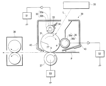
Embodiment 2
Fig. 3 schematically illustrates the
construction of an electrophotographic apparatus
provided with a process cart:ridge having a means for
feeding charging particles and having the
electrophotographic photosensitive member of the
present invention.
A drum-shaped electrophotographic
photosensitive member 31 :is rotatively driven in the
direction of an arrow at a constant: peripheral speed.
A charging roller 32 a charging means has is
constituted of charging particles 33 (conductive
particles for charging 'the electrophotographic
photosensitive member electrostatically), and a
medium-resistance la~ver (elastic layer) 32b and a
mandrel 32a which constitute a
charging-particle-holding' member. The charging
roller 32 is in contact with the electrophotographic
photosensitive member 31 in a preset elastic
deformation level to form a contact zone n.
The charging roller ~~2 in this embodiment is
constituted of the mandrel 32a and formed thereon the
medium-resistance layer 32b comprised of a rubber or
a foam, and further held on its surface the charging
particles 33.
The medium-resistance layer 32b is comprised of
CA 02414957 2002-12-20
'_ ~ 2
a resin (e. g., urethane), conductive particles (e. g.,
carbon black), a vu'ycanizing agent and a blowing
agent or the like, and is formed intro a roller on the
mandrel 32a. Thereafter, its surface is polished.
The charging roller i.n this embodiment differs
from the charging roller (charging roller for
discharging) in Embodiment 1 especially in the
following points.
(1) Surface structure and z:oughness characteristics
so designed as to hold the charging particles on its
surface in a high density.
(2) Resistance characaerist:ics (volume resistivity,
surface resistance) necessary for. injection charging.
The charging roller f-or discharging has a flat
surface, and has a surface average roughness Ra of
submicrons or less and also ~~ high roller hardness.
In the charging which utilizes discharging, a
phenomenon of discharge takes place at the gap of
tens of micrometers (fin) whi~zh is a little apart from
the contact zone between the charging roller and the
electrophotographic photosensitive member. Where the
charging roller and elect~rophotographic
photosensitive member surfaces have unevenness, the
phenomenon of discharge may become unstable because
of electric field intensit_Le;s which differ at some
parts, to cause charge non-uniformity. Hence, the
charging roller for discharging requires a flat and
CA 02414957 2002-12-20
- 63 -
highly hard surface.
The reason why the charging roller for
discharging can not. perform injection charging is
that, although the charging roller having such a
surface structure as stated above externally appears
to be in close contact with the drum
(electrophotographic photosensitive member), the two
are in almost non-contact with each other in respect
of microscopic contact performance at a molecular
level which is necessary for charge injection.
On the other hand, the charging roller 32 for
injection charging is required to have a certain
roughness because it is necessary to hold thereon the
charging particles 33 in a high density. It may
preferably have an average surface roughness Ra of
from 1 ~tm to 500 ~.t,m. If it. has the Ra of less than 1
dun, it may have an insufficient surface area for
holding thereon the charging particles 33, and also,
where any insulator (e.g., the toner) has adhered to
the roller surface layer, it is difficult that at its
surrounding area the charging roller 32 can come into
contact with the electrophotographic photosensitive
member 31, tending to lower its charging performance.
If on the other hand it has the Ra of more than 500
um, the unevenness of the charging roller surface
tends to lower the in-plane charge uniformity of the
electrophotographic photosensitive member.
CA 02414957 2002-12-20
- 64 -
The average surface roughness Ra is measured
with a surface profile analyzer microscope VF-7500 or
VF-7510, manufactured by P:eyence Co. Using objective
lenses of 1, 250 magnific:at~ions to 2, 500
magnifications, the roller surface profile and Ra can
be measured in non-contact.
The charging roller for discharging comprises a
mandrel on which a low-resistance base layer is
formed and thereafter its surface is covered with a
high-resistance layer. In the roller charging
effected by discharging, applied voltage is so high
that, if there are any pinholes (at which the support
stands uncovered because of: the damage of the film),
the drop of voltage may extend up to their
surrounding areas to cause faulty charging.
Accordingly, the charging roller may preferably be
made to have a surface resistance of 1011 S20 or more.
On the other hand, in the injection charging
system, it is unnecessary to make the surface layer
have a high resist~an~~e in order to make it possible
to perform charging at a low voltage, and the
charging roller may be constituted of a single layer.
In the injection charging, the charging roller may
preferably have a surface resistivity of from 104 to
101° S-20. If it has a surf<ice resistivity of more than
101° 520, the in-plane charge uniformity may lower,
and any non-uniformity duE: to the rubbing friction of
CA 02414957 2002-12-20
- 65 -
the charging roller may appear as lines (or streaks)
in halftone images, and a lowering of image quality
level tends to be seen. Lf on the other hand it has
a surface resistivity of less than 104 520, pinholes
of the electrophotographic photosensitive member tend
to cause the drop of voltage even in the injection
charging.
The charging roller may further preferably have
a volume resistivity ranging from 104 to 10' S2~cm. If
it has a volume resi stivity of less than 104 S2~cm,
the drop of voltage tends ~o occur because of a
leakage of electric current through pinholes. If on
the other hand it has a volume resistivity of more
than 10' S2~cm, any electric: current necessary for the
charging may be difficult to ensure, tending to cause
a lowering of charging voltage.
The resistivities of the charging roller are
measured in the following way.
To measure roller resistivities, an insulator
drum of 30 mm in outer diameter is provided with
electrodes in such a way that a i.oad of 1 kg in total
pressure is applied to the mandrf~l 32a of the
charging roller 32. As the electrodes, a guard
electrode is disposed around a main electrode to make
measurement. The distance between the main electrode
and the guard electrodE: is adjusted substantially to
the thickness of the elastic layer 32b so that the
CA 02414957 2002-12-20
- b6 -
main electrode may ensure a sufficient width in
respect to the guard electrode. In the measurement,
a voltage of +100 V is applied from a power source to
the main electrode, and electric currents flowing to
ammeters Av and As are measured, and the volume
resistivity and the surface resistivity, respectively,
are measured.
In the injection charging system, it is
important for the charging roller 32 to function as a
flexible electrode. In the case of a magnetic brush,
that is materialized in virtue of the flexibility a
magnetic-particle layer itself has. In this
embodiment, it is achieved by controlling the elastic
properties of the medium-resistance layer (elastic
layer) 32b. This :Layer may have an Asker-C hardness
of from 15 degrees to 50 degrees as a preferable
range, and from 25 degrees to 40 degrees as a more
preferable range. Ii this layer has a too high
hardness, any necessary elastic. deformation level can
not be attained, and the contact zone n can not be
ensured between tree charging roller and the
electrophotographic photosensitive member, resulting
in a lowering of ~~harging performance. Also, the
contact performance at a molecular level of substance
can not be attained, and hence any inclusion of
foreign matter may obstruct the contact at its
surrounding area. If on the other hand this layer
CA 02414957 2002-12-20
- 67 -
has a too low hardness, the shape of the roller may
become unstable to make non--uniform a contact
pressure with the charging object
(electrophotographic photosensitive member) to cause
charge non-uniformity. ~t.herwise, such a layer may
cause faulty charging due to compression set of the
roller when left standing for a long time.
Materials for the charging roller 32 may
include ethylene-propylene-dime-methylene rubber
(EPDM), urethane rubber, nitrite-butadiene rubber
(NBR) and silicone rubber, and rubber materials such
as isoprene rubber (IR) in which a conductive
substance such as carbon black or a metal oxide has
been dispersed for the purpose of resistance control.
Without dispersing any conductive substance, it is
also possible to make resistance control by using an
ion-conductive material. 'hereafter, if necessary,
the surface roughness may be adjusted, or shaping may
be made by polishing or the like. Also, a plurality
of functionally separated layers may make up the
elastic layer.
As a form of the roller, a porous-member
structure is preferable. This is advantageous in
view of manufacture in that the above surface
roughness is achievable at the same time the roller
is formed by molding. It is suitable for the porous
member to have a cell diameter of from 1 N.m to 500 ~.m.
CA 02414957 2002-12-20
- 68 -
After the porous member has been formed by foam
molding, its surface may be abraded to make the
porous surface exposed, to produce a surface
structure having the above roughness.
The charging roller 32 is provided in a stated
elastic deformation level in respect to the
electrophotographic photosensitive member 31 to form
the contact zone n. At this contact zone n, the
charging roller, which is rotatively driven i.n the
direction opposite (counter) to the rotational
direction of the electrophotographic photosensitive
member 31, can come into contact with the
electrophotographic photosensitive member 31 in the
state the former has a velocity difference in respect
to the latter's surface movement. Also, at the time
of image recording of a printer, a stated charging
bias is applied to they charging ro:Ller 32 from a
charging bias application power source S1. 'thus, the
periphery o.f the elec:trophotographic photosensitive
member 31 is uniformly electrostatically charged to a
stated polarity and ~>otential by the injection
charging system.
The charging particles 33 are added to the
toner and held in a developing assembly, and they are
fed to the charging roller 32 via the
electrophotographic photosensitive member 31 in
conjunction with development with the toner. As a
CA 02414957 2002-12-20
- 69 -
feeding means therefor, construction is employed in
which a control blade 34 is brought into contact with
the charging roller 3.' and the charging particles 33
are held between the charging roller 32 and the
control blade 34. The charging particles 33 are
coated in a constant quantity on the charging roller
32 as the electrophotographic photosensitive member
31 is rotated, and reach the contact zone n between
the charging r_oller_ 32 and the elec:trophotographic
photosensitive member 31.
The charging particles 33 may also preferably
have a partic:Le diameter of 10 ~,m or less in order to
ensure high charging efficiency and charging
uniformity. In the present invention, the particle
diameter in a case ir: which the charging particles
constitute agglomerates is defined as an average
particle diameter of t=he agglomerates. To measure
the particle diametex:~, at least 100 particles are
picked up through observation with an electron
microscope, where the volume particle size
distribution is calculated on the basis of
horizontal-di.recti.on maximum chordal length, and the
particle diameter is determined on the basis of the
50o average particle diameter.
The charging particles 33 may be present not
only in the state of primary particles, but also in
the state of agglomerated secondary particles without
CA 02414957 2002-12-20
- 70 -
any problem at a11.. Whatever the agglomeration state
is, their forms are not. important as long as the
agglomerates can f=unction as the charging particles.
The charging particles 33 may preferably be
white or closely transparent so that they do not
especially obstruct latent-image exposure when used
in the charging of the elect.rophotographic
photosensitive member. They may further preferably
be colorless or white when used in color image
recording, taking into account the fact that the
charging particles may partly inevitably be
transferred to the transfer material P from the
surface of the electrophotographic photosensitive
member 31. Also, in order to prevent light
scattering from being caused by the charging
particles 33 at the time of imagewise exposure, they
may preferably have a particle diameter which is not
larger than the size of component image pixels, and
more preferably not larger than the particle diamett=r
of the toner. The lower limit of the particle
diameter is considered to be 10 nm stably obtainable
as particles.
Reference numeral 36 denotes a developing
assembly. Electrostatic latent images formed on the
surface of the electrophotographic photosensitive
member 31 are developed as toner images by means of
this developing assembly 36 at a developing zone a.
CA 02414957 2002-12-20
- 71 -
In the developing assembly 36, a blended agent of a
toner and charging particles added thereto is
provided.
The electrophotographic apparatus (print er) in
this embodiment carries out a toner recycle process.
The transfer residual toner having remained on the
surface of the electr_ophotographic photosensitive
member 31 after transfer of toner images is not
removed by a cleaning means (cleaner) used
exclusively therefor, but is temporarily collected on
the charging roller 32 which is counter.-rotated as
the electrophotographic photosensitive member 31 is
rotated, Then, while it moves circularly around the
periphery of the charging roller 32, the toner whose
electric charges having been reversed are normalized
is successively thrown out to the electrophotographic
photosensitive member 31 and reaches the developing
zone a, where it is c~ollected at a developing means
36 by cleaning-at-development and is reused.
Reference numeral 35 denotes a laser beam
scanner (exposure means) having a laser diode polygon
mirror and so forth. This laser beam scanner 35
emits laser light intensity-modulated correspondingly
to time-sequential digital image signals of the
intended image information, and subjects the
uniformly charged surface of the electrophotographic
photosensitive member to scanning exposure L through
CA 02414957 2002-12-20
- 72 -
the laser light. As a result of this scanning
exposure L, electrostatic latent images corresponding
to the intended image information are formed on the
surface of the electrophotographic photosensitive
member 31. The electrostatic latent images thus
formed are developed by the developing means 36 to
form toner images. To the developing means 36, a
developing bias is app lied from a power source S2.
Reference numeral 38 denotes a fixing means of,
e.g., a heat fixing system. A transfer material P
which has been fed to a transfer contact zone b
between the electrophotographic photosensitive member
31 and a transfer_ roller 37 and to which the toner
images have been transferred under application of a
transfer bias from a power source S3 is separated
from the surface of the electrophotographic
photosensitive member 31. It is then guided into
this fixing means 38, where the toner images are
fixed, and then put out of the apparatus as an
image-formed matter (a print or a copy).
Reference numeral. 39 denotes a process
cartridge which, in this embodiment, is constituted
of the electropriotographic photosensitive member 31,
the charging roller 32 and the developing assembly 36
which are integrally supported together in the
cartridge, and is detachably mountable on the main
body of the apparatus through a guide means such as
CA 02414957 2002-12-20
- 73 -
rails 40 provided in the main body of the apparatus.
The electrophotographic photosensitive member of
the present invention may be not only applied in
electrophotographic copying machines, but also widely
applied in the fields where electrophotography is
applied, e.g., laser beam printers, CRT printers, LED
printers, facsimile machines, liquid-crystal printers,
and laser platemaking.
Examples of the present invention are given
below. The present invention is by no means limited
to the following Examples. In the following Examples
and Comparative Examples, "part(s)" refers t.o
"part(s) by weight".
Example 1
On an aluminum cylinder as a conductive support,
having an outer diameter of 30 mm and a length of 261
mm, a 5% by weight methanol solution of a polyamide
resin (trade name: AhIILAN CM8000; available from
Toray Industries, Inc.) was applied by dip coating,
followed by drying to form a binding layer with a
layer thickness of 0.5 Eun.
Next, 3.5 parts of hydroxyga:Llium phthalocyanine
crystals having strong peaks at Bragg's angles (28 ~
0.2°) of 7.4° and 28.2° in the CuKa characteristic
X-ray diffraction and 1 part of polyvinyl butyral
resin (trade name: S-LEC BX-1; available from Sekisui
Chemical Co., Ltd.) were added to 120 parts of
CA 02414957 2002-12-20
- 74 -
cyclohexanone, and these were dispersed for 3 hours
by means of a sand mill making use of glass beads of
1 mm in diameter, and diluted by further addition of:
120 parts of ethyl acetate to make a charge
generation layer coating dispersion.. This coating
dispersion was applied onto the above binding layer
by dip coating, followed by drying at 100°C for 10
minutes to form a charge generation layer with a
layer thickness of 0.15 dun.
A powder X-ray diffraction pattern of the
hydroxygallium phthalocyanine crystals is shown in
Fig. 4. The powder X-ray diffraction was measured by
using CuKa, radiations under the fo_Llowing conditions.
Measuring instrument used: Full-automatic X-ray
diffractometer MXP18, manufactured by Mach Science Co.
X-ray tube: Cu
Tube voltage: 50 kV
Tube current: 300 mA
Scanning method: 28/A scan
Scanning speed: 2 dec~./min.
Sampling interval: 0.020 deg.
Start angle (26): 5 deg.
Stop angle (26): 40 deg.
Divergent slit: 0.5 deg.
Scattering slit: 0.5 deg.
Receiving slit: 0.3 deg.
Curved monochromator was used.
CA 02414957 2002-12-20
- 75 -
Next, as a charge-transporting material 10 parts
of a compound having structure represented by the
following formula:
H3C \ / \ /
N ~ ~ CH=C
\ / \
and as a binder resin 10 parts of bisphenol-c,
polycarbonate (trade name: IUPILUN Z-200; available
from Mitsubishi Gas Chemical Company, Inc.) were
dissolved in a mixed solvent of 100 parts of
monochlorobenzene to prepare a charge transport layer
coating solution. This coating solution was applied
onto the charge generation :Layer, and dried with hot
air at 105°C over 1 hour to form a charge transport
layer 20 urn thick.
Next, 20 parts of anta_mony-doped ultrafine tin
oxide particles surface-treated with a compo,and
(amount of treatment: 70) having structure
represented by the following formula:
CA 02414957 2002-12-20
- 76 -
~J-CH3
F3C-CH2 CH2 Si-fJ--CH3
a-CHI
30 parts of antimony-doped fine tin oxide particles
surface-treated with methylhydrogen silicone oil
(trade name: KF99; available from Shin-Etsu Chemical
Co., Ltd.) (treatment amount: 20°>) and 150 parts of
ethanol were dispersed by means of a sand mill over a
period of 66 hours, and 20 parts of fine
polytetrafluoroethylene particles (average particle
diameter: 0.18 Vim) were further added, followed by
dispersion for 2 hours. Thereafter, in the resultant
dispersion, 30 parts of resol type heat-curable
phenolic resin (tirade name: PL-4804; containing an
amine compound; available from Gunei Kagaku Kogyo
K.K.) was dissolved as a resin component to prepare a
coating solution for a protective layer.
This coating solution was applied onto the charge
transport layer, and dried with hot air at 145°C over
1 hour to form a protective layer.
The thickness of this protective layer was
measured by the use of an instantaneous multi-
photometry system MCPD-2000 (manufactured by Ohstuka
Denshi K.K.) utilizing light interference, and found
to be 3 ~,m. Dispers:ibility of the coating solution.
CA 02414957 2002-12-20
77
for the protective layer is desirable, and the visual
detection of the protective layer surface showed that
the surface was free o.f unevenness and uniform.
The Vsl(0.2) and Vsl(0.5) of the resulting
electrophotographic photosensitive member were
measured with a drum testing machine (manufacaured
Jentech Co.). In the measurement, the
electrophoptograohic photosensitive member surface
was charged to -700 V under the 23 °C/5% RH
environment, and irradiated with white light in the
light quantity of 10 lux~sec. A potential-measuring
probe was set at positions of 90° and 224.5 from the
position where the white light was irradiated, and
the probe at the 90° position and the probe at the
224.5° position measured the Vsl(0.2) and the
Vsl (0.5) , respectively.
The above-obtained electrophotographic
photosensitive member- was mounted on a remodeled
apparatus of the elec:trophotographic apparatus (trade
name: Laser Jet 4000, manufactured by Hewllet-Pachard
Co.) that was in the same system as in the above
embodiment 1, and image evaluation was made. The
principal remodeling point was in that the system was
so constructed as to be the same as in the above
embodiment 2.
The charging particles had a volume resistivity
of 1 ~2~cm and the carried amount at the initial stage
CA 02414957 2002-12-20
_ 78 _
was 5 mg/cm2. The voltage applied to the charging
member from the power source S1 was only a DC voltage
of -700 V.
Under the above c:ondit.ions, the dark portion
potential (Vd) at the initial stage was measured in a
normal temperature and low humidity environment (23
°C/5$ RH). The image;> obtained were evaluated by
visual observation. In addition, for durability
tests, evaluation was made by visual observation on
images obtained after carrying out. 5,000-sheet image
formation under a normal temperature and low humidity
environment (23 °C/5° RH) and a high temperature and
high humidity environment (32 °C/85° RH). When the
durability test was carried out, a letter image with
a print rate of 6o was used, and when the evaluation
was made, an image was used in which a portion
corresponding to the first 1/3 rotation of the
photosensitive member_ is solid black and the
remaining portion is of a half-tone comprised of
dotted lines arranged every second line in which each
of the dotted lines is composed of black dots of
1,200 dpi arranged every second dot and the dot
arrangements of adjacent dotted lines are opposite to
each other.
The evaluation results are shown in Table 1.
Example 2
The electrophotographic photosensitive member
CA 02414957 2002-12-20
- 79 _
was evaluated in the same way as in Example 1 except
that the electrophotographic apparatus was used
without being remodeled into the construction in the
embodiment 2. The results obtained are shown in
Table 1.
Examples 3 and 4
Eelectrophotographic photosensitive members
were made in the same way as in Example 1 except that
the resole-type phenol resin (trade name: PL-4804)
was changed to each of a resole-type phenol resin PL -
4852 (produced by Gunei Kagaku Kogyo K.K., containing
an amine-type compound) (Example 3) and a resole-type
phenol resin PL-5294 (produced by Gunei Kagaku Kogyo
K.K., containing an alkaline metal) (Example 4). The
results obtained are shown in Table 1.
Examples 5 and a
The electrophotographic photosensitive member
was evaluated in the ~~ame way as in Examples 3 and 4
except that the electnophotographi~ apparatus was
used without being remodeled into the construction in
the embodiment 2. The results obtained are shown in
Table 1.
Examples 7 and 8
An electrophotographic photo.>ensitive member
was made in the same way as in Example 1 except that
the resole-type phenol resin (trade name: PL-4804)
was changed to a bisphenol A-type epoxy resin (trade
CA 02414957 2002-12-20
_ 80 -
name: 8309, produced by Mitsui Petrochemical
Industries, Ltd.), the solvent was changed from
ethanol to tetrahydrofuran, and the coating method
for forming the protective layer was changed from the
dipping method to a spray coating method, and
evaluations in Examples 7 and 8 were made in the same
way as in Examples 1 and 2, respectively. The
results obtained are shown in Table 1.
Examples 9 and 10
An electrophotographic photosensitive member
was made and evaluated in the same way as in Examples
7 and 8 except that the amount of bisphenol A-type
epoxy resin used was changed from 30 parts t:o 40
parts. The results obtained are shown in Table 1.
Examples 11 and 1'?
An electrophotographic photo:>ensitive member
was made and evaluated in the same way as in Examples
9 and 10 except t=hat. the thickness of the protective
layer was changed from 3 ~.~.m to 5 ~t:m. The results
obtained are shown. irn. Table 1.
Examples 13 and I4
An elect.rophotographic photosensitive member
was made and evaluatF~d in the same way as in Examples
9 and 10 except that the thickness of the protective
layer was changed from 3 um to 5.5 ~.m. The results
obtained are shown in Table 1.
Comparative Examples 1 and 2
CA 02414957 2002-12-20
- 81 -
An electrophotographic photosensitive member
was made and evaluated in the same way as in Examples
9 and 10 except that the amount of bisphenol A-type
epoxy resin used was changed from 40 parts to 50
parts and the thickness of the protective layer was
changed from 3 E~m to 6. '.~ Win. The results obtained
are shown in Table 1.
Comparative Examples 3 and 4
An electrophotographic photosensitive member
was made and evaluated in the same way as in Examples
7 and 8 except that the amount of bisphenol A-type
epoxy resin used was changed from 30 parts to 55
parts. The results obtained are shown in Table 1.
Comparative Examples 5 and 6
An electrophotographic photosensitive member
was made and evaluated in the same way as in Examples
7 and 8 except that the amount of bisphenol A-type
epoxy resin used was changed from 30 parts to 10
parts. The results obtained are shown in T<~ble 1.
Example 15
An electrophotographi.c photosensitive member
was made and evaluated in the same way as in Example
5 except that instead of adding tin oxide particles,
parts of a charge transporting material
25 represented by the following formula was added to
form the protective layer. The results obtained are
shown in Table 1.
CA 02414957 2002-12-20
- 82 -
HO-H~CH~C ~
_ N ~ ~ CH2CH~ OH
HO-H2CH2C ~
Example 16
An electrophotographic; photosensitive member
was made and evaluated in the same way as in Example
15 except that the resole-type phenol resin {trade
name: PL-4852) was changed to a curable siloxane
resin KP-854 (produced by Shin-Etsu Chemical
Co.,Ltd.). The results obtained are shown in Table 1.
Example 17
An electrophotog raphic photosensitive member
was made and evaluated in the same way as in Example
16 except that the thickness of the protective layer
was changed from 3 ~1m to 5.5 ~.un. The results
obtained are shown iri Table 1.
Comparative Example 7
An electrophotographic photosensitive member
was made and evaluated in the same way as in Example
16 except that the amount of curable siloxan.e resin
used was changed from 30 parts to 40 parts a.nd the
thickness of the protective layer was changed from 3
~.un to 6.5 dun. The results obtained are shown in
Table 1.
Comparative Example 8
An electrophotographic photosensitive member
CA 02414957 2002-12-20
was made and evaluated in the same way as in Example
16 except that the amount of charge-transporting
material added was changed from 30 parts to 70 parts.
The results obtained are shown in Table 1.
Comparative Example 9
An electrophotographic photosensitive member
was made and evaluated in the same way as in Example
16 except that the amount of charge-transporting
material added was changed from 30 parts to 10 parts
IO and the thickness of the protective layer was changed
from 3 Eun to 6.5 Eun. The results obtained are shown
in Table 1.
Comparative Example 10
An electrophotographic photosensitive member
was made and evaluated in the same way as in Example
17 except that as a charge-generating compound used
was a hydroxytitanium phthalocyanine crystal_ having
intense peaks at 7.6°, 10.2°, 25.3° and 28.F° of
the
Bragg angle (28 ~ 0.2°) in CuKa characteristic X-ray
diffraction. The results obtained are shown in Tab.Le
1.
Example 18
An electrophotographic photosensitive member
was made and evaluated in the same way as in Example
7 except that the voltage applied to the charging
roller was changed from the only DC voltage to a
voltage composed of a DC voltage of -700 V superposed
CA 02414957 2002-12-20
- 84 -
on an AC voltage whose peak-to-peak voltage is 500 V.
The results obtained are shown in Table 1.
Comparative Example 11
An electrophotographic photosensitive member
was made and evaluated in the same way as in
Comparative Example 2 except that the voltage applied
to the charging roller was changed from the only DC
voltage to a voltage composed of a DC voltage of
-700 V superposed on an AC voltage whose peals-to-peak
voltage is 500 V. The results obtained are shown in
Table 1.
Comparative Example 12
An electrophotographic photosensitive member
was made and evaluated in the same way as in Example
16 except that the amount of curable siloxane resin
used was changed from 30 parts to 45 parts and the
thickness of the protective layer was changed from 3
Eun to 2 ~.m. The results obtained are shown in Table
1.
CA 02414957 2002-12-20
_ 8!~ _
+~ +~
m cn u~ <n m u~
~n
~
~
~
,. .
~ .
>~ n
.
zs ~ ~ ts~ :s is
zs
a~ a~ ~ a~ a~ a~
a~
V'
.
1-~ ~ '~ -f'~ -~
'~
f-
1
.~...I
.~
-.-I~ -.-1 O O O O O O O -I ~-I r-I -I
O r-I r-I r1 O
O O
O x C7 C7 C~ U t~ C7 u) cn v) v7
C7 C~ v) U) cn C7 C7
C~
. . . .
r0 +~ +-~ a..i
.1-~
N O O O O
.c: .~
o tr :s is
is
-.-I r1 -r-I -.-~
U1 +~ .7~ r-I
+~
l-~
-ri -r-I ~ ri
-r-I U7 fn LT
U7
+~ 'b O O N O
!~
S-1.~-, .S-~. .~ .i.
.f:.
'
b
+~ 3 O O O O O O O O O O -~-I -~
O O -.--I -r-I
O O
4-IO O O O O O O O O O O ~-i --I
O O rl O r-I
O
r..~r-a C'J U C'J L7 C~ C'J C7 C.7 C!7
C'J C'~' C-7 C'~ C~ C/7 Ul
C'J rJ
N
r1
E-i _
N
O
O W ~> ~7 O W un CO 00 O O O
r-1 O ~' lO lO O N ~f)
J r-I ,-I N <V N N N M ~-1
c-1 M N N ri M
r1 N
,...
~
I
N
O O lfl CO O O t~ !~ Cw O O
~ O ~9 V' ~' l~ M O
'J ~' d' M M M M d' ~' cr t~' c-1
O M M <f' ~' M M
r7
I I I I I I I I I I I I I I
I I I I
O
N
if7 in GO Wn O ~W n C'~ O O
W O O O f~ U7 ~~
O un ~n l0 u7 tn I' I~ l~ I~ N lWn
tn C- t~ C' I I
I I I I I 1 I I t I I I I
I I I
I
U~r-I~ 'O 't~ '~ "C~ '~ '~ 'C~ 'z3
'~S 't3 "O 'z3 b 'D b
b 'L3 'C~
u~~ rt3O O O O O O O O O O O O O O
O O O O O
~-rl O O O O O O O O O O O O O
O O O O O
--IH O+~ CJ C~ C~ ;~ C7 C~ C~ U U"
CJ C_7 C7 C7 C~ C7 C7
CJ C~
tt~
+~ 00000 00000 oumnoo oom
.b~ cr a0 c0 a~ c0 ~ r~ ~.9 o~
.. ~ a~ a0 o~ I~ c0 0o
a0 a~
~ ., mm ~n ~m ~n u, m ~n m mn
y u ~m u~
H r--I I I I I I I I I I I 1 I I
I I I I I
I~
y -I N M l0 t~ 00 ~ ~
V' W 01 ~
~1 ~ '-1 ri
rl
I W
CA 02414957 2002-12-20
_ 8 ~;
~ ~ ~~ +~ ~ ~ +~
fn U7 U1 U7 U7 In
O O O O O O O
-r-I .~ .~ .L:
'O LT is :_nU~ is is Cs
a) a) a) N Q) a) a)
-G -ri -ri -ri-rl -ri -r-1 -r-1
~ . . .N
C,' -ri -r1 -r-i-r1'-C~'~ -ri'b '~ -r~ -ri
. U7 u1 U1 U1 O O U) O O U7 U7
- O O O O O O O O O O I
l O
r I1, !n Oa (n C~ C~ P-W~ C7 W
U ~ . .
J--)~~ 1~ ~~ ~ +? +-~1~ 1-~~J
-,-I ~n u W7 u7 cn m u7 cn cn US
I--Icn O O O O O O O O O O
.L:.LS.~~ ~ .s:.~ ~ .~ .~ .s~
N -rl LT Ct~C3~ tT is tT b~ Ls is Cs
x -ri a~ a~ (v a~ a~ as a~ a~ a~ a~
a~~ ~ ;> ~ ~ ~ a
..~-r-i-.-I-.1-r-I-ri -rl-r1-r-i-r1
~-I~ ~ ~-J1-~ ~7 +-1.S->.1-)~ J-)-1-)
~
. -rl-,-I-~-I-r-If0 fIf -ri(C3(>~-r-1 'O
;~ +~3 u~ m (n cn ~ :3~ cn is a~ cn O
4--IO O O O O a) a) O a) a) O I O
w as a~ w ;~ ~. as z z w c~
c~
O
t>
r-.i I N
O
O N N Lf7 LI7~p p~ Lf~~ (17Lf~ N M
-- J M M f'~ M f''1 r-IM M M
--I
,
~
U)
O
E.1
-I
r~
CO O~ <J <J <V N ~ pf)O O 00 N
'J V d' V' lI) Lf>r-Ir--IM I 00 Lf) '.~'N
O I I G I I I I I
I I I
--~
N O O W Ii O O O N ~ Ln O LG
~ O~ ~b - N CJ (~ [-iOl 00 O~ tl~
I I I CO I I I I I I I I
I
Q; a)
.
. -r'I
r1 .
. . . . ~
. '
'
-y~is tip'L~"O ri U1 tn 'C3 'O T3 fa U1 U C5~
r-1 -W '~ C3 O
S~
m In x o o ~n o 0 0 0 o is o r~ fa
ra u) 0 o o
o
0 0 0 .~ .~ 0 0 o a~ .~ .-I~
o 0 o o
~ C7 C7 0.~ is is C~ C~ C7 Z ~ W -rl
+~ Ci,C~ C7 C7
rr~ N
-r-I
I-~ ~ -,~Lf~O O C~ O O O O O O O O
t~ r~ ~ r- 01 00 ~ o~ oo r- O o0
~
Lf~LI]Lf) LI7Lf)Lf~ LI LI)LIBLl7 r-1Ln
7 I I I I I
H ~ I I I I 1 I I
c0
r--IN M a' t1)IS W~ O~ Ol O r-IN
U
CA 02414957 2002-12-20
87 _
As stated above, the present invention has made
it possible to provide the electrophotographic
photosensitive member i~hat c an stably provide high
grade images which have almost no positive ghosts and
negative ghosts caused by extensive operation in
repeated use and also are fwee of blurred images, and
the process car_tr.idge ar.d el.ectrophotographic
apparatus having that el.ectrophotographic
photosensitive member.