Note: Descriptions are shown in the official language in which they were submitted.
CA 02415495 2003-O1-08
1
(Title of the Invention)
SILICON OXIDE FILM
(Technical Field to which the Invention Belongs)
The present invention relates to a silicon oxide
film formed on the surfaces of a plastic substrate.
More specifically, the invention relates to a silicon
oxide film which has excellent gas shut-off property and
is useful in a field of packing materials.
(Prior Art)
As packing containers, there have heretofore been
used metal cans, glass bottles and a variety of plastic
containers. Among them, plastic containers have such
advantages that they are light in weight and are
excellent in shock resistance to some extent
accompanied, however, by such problems as permitting the
contents to be degenerated and flavor to be decreased
due to oxygen that permeates through the container
walls.
In metal cans and glass bottles, in particular, no
oxygen permeates through the container wall, and what
causes a problem is only the oxygen remaining in the
containers. In the case of plastic containers, on the
other hand, oxygen permeates through the container walls
to a degree that is no longer negligible arousing a
problem from the standpoint of preserving the contents.
In order to prevent this, there has been proposed a
plastic container having a container wall of a multi-
layer structure at least one of the layers being formed
of an oxygen-blocking resin such as an ethylene/vinyl
alcohol copolymer.
However, a multi-layer plastic container requires a
technology such as co-extrusion or co-injection of a
plurality of resins, a cumbersome formation operation as
compared to forming a single-layer resin container,
CA 02415495 2003-O1-08
7
accompanied by a problem of low productivity.
It has also been known. already to improve the gas
shut-off property by forming a film by vapor deposition
on a plastic material of a single layer, and to form a
silicon oxide film (SiOx) as well as to form a hard
carbon film (DLC).
Japanese Unexamined Utility Model Publication
(Kokai) No. 50563/1974 and Japanese Unexamined Patent
Publication (Kokai) No. 58171/1974 are teaching silicon
oxide films by coating a plastic film based on a
physical vaporization method (PVD).
Further, Japanese Unexamined Patent Publication
(Kokai) No. 345383/1993 teaches a silicon oxide film
formed by the chemical vaporization method (CVD).
Japanese Patent No. 2526766 filed by the present
applicant discloses a gas-blocking laminated plastic
material comprising a plastic member, a first layer of a
polymer formed thereon and containing not less than 150
of silicon, not less than 200 of carbon and the
remainder of oxygen, and a second layer of a silicon
oxide film formed on the first layer.
However, the conventional silicon oxide film must
have a considerably large thickness to impart the
required gas shut-off property. Besides, the coated
film lacks adhesion to the plastic substrate, softness
and flexibility. When, for example, the plastic
substrate coated with the above film is drawn, the film
is subject to be broken. The productivity is poor,
either.
In particular, the silicon oxide film formed by the
physical vaporization method (PVD) has inferior oxygen
gas shut-off property as compared on the basis of the
same film thickness. To achieve the gas shut-off
property of the same level, therefore, the film must be
formed maintaining a considerably large thickness.
CA 02415495 2003-O1-08
Disclosure of the Invention
It is therefore an object of the present invention
to provide a silicon oxide film having particularly
excellent gas shut-off property (gas barrier property),
capable of excellently shutting off gases with a small
film thickness as compared to the conventional films,
the film that is deposited exhibiting excellent adhesion
to the plastic substrate, softness and flexibility,
lending itself well for being excellently produced.
According to the present invention, there is
provided a silicon oxide film formed on the surfaces of
a plastic substrate, wherein methyl groups and methylene
groups are contained in the silicon oxide film in a
portion near the interface to the plastic substrate.
The fact that the methyl groups and the methylenes
group are existing in the silicon oxide film of the
invention in a portion close to the interface to the
plastic substrate, can be confirmed by, for example,
depositing an Al film on the surface of the silicon
oxide film formed on the surface of the plastic
substrate, eluting the plastic substrate by using an
organic solvent such as hexafluoroisopropanol or the
like, and measuring a first infrared absorption spectrum
of the surface of the remaining silicon oxide film.
That is, in the first infrared absorption spectrum, an
infrared absorption peak due to the methyl group and an
infrared absorption peak due to the methylene group
appear in a region of wave numbers of from 2800 to 3000
cm-1. These peaks make it possible to confirm the
presence of the methyl groups and methylene groups.
Further, the first infrared absorption spectrum contains
an infrared absorption peak due to Si0 in a region of
wave numbers of prom 1000 to 1300 cm 1 and, particularly,
near 1200 cm-1.
By using a secondary ion mass analyzer (SIMS),
CA 02415495 2003-O1-08
4
further, distributions of SiCH~ ions and SiCHs ions in
the film from the outer surface of the silicon oxide
film toward the surface of the substrate are measured to
make sure the positions where the S;_CH2 ions and SiCH3
ions due to an organosilicon compound polymer are
present, from which it is obvious that they are not
existing on the outer surface of the film but are
existing near the interface to the plastic substrate.
That is, in the silicon oxide film of the present
invention, the organic groups (methyl groups and
methylene groups) are existing near the interface to the
plastic substrate accounting for excellent adhesion to
the plastic substrate and flexibility. Even when the
plastic substrate is intensely drawn, therefore, the
film is effectively prevented from being broken.
In the present invention, further, the silicon
oxide film has a two-layer structure comprising a first
layer positioned on the side of the interface to the
plastic substrate and a second layer on the first layer
(i.e., layer positioned on the front surface side of the
film). The methyl groups and the methylene groups are
more distributed in the first layer than in the second
layer. It is desired that the methyl groups and the
methylene groups are not substantially contained in the
second layer.
In the second infrared absorption spectrum of the
silicon oxide film of the invention, for example, it is
desired that an absorption peak exists in a region of
wave numbers of from 1215 to 1250 cm 1. The second
infrared absorption spectrum is measured by the
multiplex reflection differential spectral method from
the film surface (surface of the second layer). The
above first infrared absorption spectrum chiefly
represents infrared absorption characteristics of the
first layer positioned near the interface to the plastic
CA 02415495 2003-O1-08
substrate while the second infrared absorption spectrum
chiefly represents infrared absorption characteristics
of the second layer.
That is, owing to the above-mentioned two-layer
structure, the silicon oxide film of the present
invention exhibits excellent gas shut-off property.
in the second infrared absorption spectrum of the
silicon oxide rilm, further, it is desired that the
absorbency rat~_o defined by the following formula (1),
Ri = A1 /A2 x 100 -- ( 1 )
wherein A1 is an area of an absorbency of wave
numbers over a range of from 1215 to 1250 cm-1, and
Az is an area of an absorbency of wave numbers over
a range oz from 985 to 1250 cm 1,
is not smaller than 10.
In the second infrared absorption spectrum of the
silicon oxide film of the present invention, further, it
is desired that the infrared absorbency ratio of
SiOH/Si0 is not larger than 0.25.
It is desired that the silicon oxide film of the
present invention has a silicon distribution coefficient
represented by a ratio of the silicon content and the
film thickness (silicon content/thickness) of 0.3 g/cm3,
has an oxygen permeation coefficient of not larger than
0.5 x 10 16 CC ' cm/cmz/sec/cmHg (30° C) and, further, has
a 10-point average surface roughness (Rz) of smaller
than 25 nm and a center line average roughness (Ra) of
smaller than 10 nm.
The silicon oxide film of the present invention
having the above properties can be produced by a plasma
CVD method and, usually, has a thickness of as very
small as from 2 to 500 nm yet exhibiting excellent gas
shut-off property.
According to the present invention, further, there
is provided a gas-blocking plastic material having an
CA 02415495 2003-O1-08
6
inner layer and an outer layer of a thermoplastic resin,
and an oxygen-absorbing layer between the inner layer
and the outer layer, wherein the above silicon oxide
film is formed on the surface of the inner layer and/or
on the surface of the outer layer.
That is, upon forming the silicon oxide film on the
inner surface and/or on the outer surface of the plastic
substrate having the oxygen-absorbing layer as described
above, there are imparted oxygen shut-off effect due to
the oxygen-absorbing layer as well as gas shut-off
property due to the silicon oxide film, making it
possible to strikingly improve the gas shut-off
property.
(Brief Description of the Drawings)
Fig. 1 is a diagram illustrating a first IR
spectrum of a silicon oxide film of the invention
prepared according to Example 1 as measured from the
side of the plastic substrate (PET bottle);
Fig. 2 is a diagram illustrating a second IR
spectrum of the silicon oxide film of the invention
prepared according to Example 1 as measured from the
side of the surface thereof (surface of the side
opposite to the interface to the plastic substrate);
Fig. 3 is a diagram illustrating the distribution
of ion concentrations in the silicon oxide film of the
invention prepared according to Example 1 as measured by
the SIMS;
Fig. 4 is a chart of an X-ray photoelectron
spectral analysis of the silicon oxide film of the
invention prepared according to Example l;
Fig. 5 is a diagram illustrating the distribution
of bonding energy of silicon in the silicon oxide film
of the invention prepared according to Example 1 in the
direction of substrate from the outer surface of the
film as measured by the X-ray photoelectron spectral
CA 02415495 2003-O1-08
7
analysis;
Fig. 6 is a diagram illustrating a second IR
spectrum of the silicon oxide film of the invention
prepared according to Example 3 as measured from the
side of the surface thereof (surface of the side
opposite to the interface to the plastic substrate);
Fig. 7 is a diagram illustrating a second IR
spectrum of the silicon oxide film of the invention
prepared according to Comparative Example 3 as measured
from the side of the surface thereof (surface of the
side opposite to the interface to the plastic
substrate);
Fig. 8 is a diagram plotting a relationship between
the SiOH/Si0 absorbency ratio (A) along the abscissa and
the oxygen permeation amount along the ordinate of
various silicon oxide films formed on the surface of the
plastic substrate (PET bottle);
Fig. 9 is a diagram illustrating a relationship
between the silicon distribution coefficient (ratio of
the silicon content in the film and the film thickness)
and the oxygen permeation coefficient of various silicon
oxide films formed on the surface of the plastic
substrate (biaxially drawn PET sheet);
Fig. 10 is a diagram schematically illustrating the
arrangement of an apparatus for treatment with a
microwave plasma used for forming the silicon oxide film
of the invention; and
Fig. 1i is a diagram illustrating the arrangement
of a plasma processing chamber in the apparatus of Fig.
10.
(Best Mode for Carrying Out the Invention)
The silicon oxide film of the present invention has
an important feature in that methyl groups and methylene
groups are existing near the interface to the plastic
substrate.
CA 02415495 2003-O1-08
g
That is, referring to Fig. 1 illustrating the first
infrared absorption spectrum, of the silicon oxide film
of the present invention of a portion near the interface
to the plastic substrate, the silicon oxide film being
prepared according to Example 1 appearing later, there
are recognized infrared absorption peaks due to the
methyl group and an infrared absorption peak due to the
methylene group in a region of wave numbers of from 2800
to 3000 cm-1 (in Fig. 1, peaks at 2857 cm 1 and 2960 cm 1
are those due to the methyl group (CH3), and a peak at
2928 cm 1 lying therebetween is the one due to the
methylene group (CHz)).
Further, the spectrum of Fig. 1 indicates a peak
due to Si0 (siloxane) in a region of wave numbers of
from 1000 to 1300 cm 1 and, particularly, near 1200 cm 1.
This fact tells that the silicon oxide film of the
present invention contains a silicon oxide as well as a
polymer of an organosilicon compound near the interface
to the plastic substrate. That is, due to the presence
of the polymer component near the interface to the
plastic substrate, the silicon oxide film is highly soft
and flexible exhibiting excellent adhesion to the
plastic substrate. As a result, excellent gas shut-off
property is exhibited despite the film has a very small
thickness.
In this invention, the portion of the silicon oxide
film near the interface to the plastic substrate varies
depending upon the thickness of the film and cannot be
definitely stated. Usually, however, this portion lies
3p in a range of not larger than 10 nm from the surface of
the plastic substrate.
It is further desired that the silicon oxide film
of the present invention has a two-layer distribution
structure. When divided into the first layer located on
the side of the interface to the plastic substrate and
CA 02415495 2003-O1-08
9
the second layer on the first layer (i.e., layer located
on the surface of the side opposite to the interface to
the plastic substrate), the methyl gro~~ps and the
methylene groups are distributed in large amounts in the
first layer, but are distributed in small amounts or are
not distributed in the second layer.
That is, the gas barrier property is improved owing
to the two-layer distribution structure in which the
methyl groups and the methylene groups are mainly
distributed in the first layer. For example, if the
methyl groups and methylene groups are much distributed
in the second layer, too, the gas barrier property tends
to be deteriorated.
The above two-layer distribution structure of the
silicon oxide film of the present invention can be
confirmed even by the SIMS (secondary ion mass spectrum)
or the X-ray electron spectral analysis.
Fig. 3 is a diagram illustrating the distribution
of ion concentrations in the silicon oxide film prepared
according to Example 1 as measured by the SIMS.
According to Fig. 3, the peaks of SiCH3 ion and SiCH2 ion
distributions are deviated toward near the interface to
the plastic substrate (PET bottle), and these ions are
not almost distributed in the surface of the film.
Further, the Si ions are sharply decreasing near the
interface to the plastic substrate.
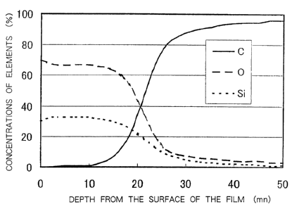
Fig. 4 is a chart of an X-ray photoelectron
spectral analysis of the silicon oxide film prepared
according to Example 1. According to Fig. 4, the
concentrations of silicon (Si) and oxygen (0) are
gradually decreasing near the interface to the plastic
substrate while the concentration of carbon (C) is
sharply increasing near the interface to the plastic
substrate. That is, it is confirmed that the film has,
on the front surface side thereof, a second layer in
CA 02415495 2003-O1-08
which no carbon (C) is substantially existing, and has,
near the interface to the plastic substrate, a layer in
which silicon (Si) is existing at a concentration of not
lower than 15o and carbon (C) is existing at a
$ concentration of not lower than 200.
Fig. 5 is a diagram illustrating the distribution
of bonding energy of silicon in the silicon oxide film
prepared according to Example 1 in the direction of
substrate from the outer surface of the film as measured
10 by the X-ray photoelectron spectral analysis. It is
confirmed from Fig. 5 that the bonding energy of silicon
on the outer surface of the silicon oxide film is near
103.5 eV due to the Si0 bond, and the bonding energy of
the layer containing not less than 150 of silicon and
not less than 200 of oxygen is changing to near 102.5 eV
due to the Si(R) - 0 bond (R is an alkyl group)
manifesting that this layer is an organosilicon polymer
layer.
It will thus be comprehended that the silicon oxide
film of the present invention has a two-layer
distribution structure having an organosilicon polymer
layer as a first layer near the interface to the plastic
substrate and a second layer on the surface thereof
without almost containing the organosilicon polymer
component but containing a silicon oxide at a very high
density.
In the present invention as shown in Fig. 2,
further, absorption peaks are existing in a region of
wave numbers of from 1215 to 1250 cm 1 in the second
infrared absorption spectrum of the silicon oxide film
obtained by the multiplex refraction differential
spectral method. Like the peak near 1200 cm 1 in the
first infrared absorption spectrum, the above absorption
peaks are locked and stem from a dense SiO. It is
considered that such a dense Si0 bond is formed in the
CA 02415495 2003-O1-08
11
silicon oxide film of the present invention probably
because a silanel group is formed and is dehydrated in
the step of forming the film as represented by the
following formula,
$ Si. - OH -~ ~ Si0
In the second infrared absorption spectrum (see
Fig. 2) of the silicon oxide film of the invention,
further, it is desired that the absorbency ratio (Ri) as
defined by the following formula (1),
Ri = Ai/Az x 100 --- (1)
wherein Al is an area of an absorbency of wave
nt:.mbers over a range of from 1215 to 1250 cm-1, and
Az is an area of an absorbency of wave numbers over
a range of from 985 to 1250 cm 1,
is not smaller than lo. The absorbency ratio (Ri) which
is not smaller than 1o means that vivid peaks exist in a
region of wave numbers of from 1215 to 1250 cm l, and a
dense SiOx exists in larger amounts as A1 increases
exhibiting excellent gas shut-off property. When the
absorbency ratio (Ri) is smaller than 10, the gas
barrier property may decrease.
In the second infrared absorption spectrum of the
silicon oxide film obtained by the multiplex reflection
differential spectral method of Fig. 2, further, it is
desired that the infrared absorbency ratio (A) of
SiOH/Ai0 is not larger than 0.25. That is, in Fig. 2,
the infrared absorption peak of SiOH is appearing over
the wave numbers of from 910 to 950 cm i and the infrared
absorption peak of S0 (siloxane) is appearing over 1020
to 1080 cm-1. When the peak ratio is not larger than
0.25, the film exhibits markedly improved oxygen gas
shut-off property. Fig. 8 is a diagram plotting a
relationship between the infrared absorbency ratio (A)
of the second layer along the abscissa and ~he oxygen
permeation amount along the ordinate of various silicon
CA 02415495 2003-O1-08
12
oxide films formed on the PET bottle. According to Fig.
8, the oxygen permeation amount monotonously increases
with an increase in the infrared absorbency ratio (A) of
SiOH/Si0 (i.e., with an increase in the amount of SiOH).
$ There exists a point of inflection at where the
absorbency ratio (A) is about 0.25. In a region not
higher than this point, the oxygen gas shut-off property
can be markedly improved.
Being related to that the silicon oxide film of the
present invention has the above two-layer distribution
structure, the silicon distribution coefficient
represented by a ratio of the silicon content in the
film/thickness of the film is not smaller than 0.3 g/cm3
and that the oxygen permeation coefficient is not larger
than 0.5 x 10 16 CC ' cm/cm2/sec/cmHg (30°C) . That is, the
silicon oxide film has a thickness which is usually as
very small as from 2 to 500 nm, and exhibits very
excellent gas shut-off property owing to the
characteristics of the above two-layer distribution
structure. By utilizing the formula of gas permeation
related to the laminate, the oxygen permeation
coefficient of the silicon oxide film is found as
follows:
t/P = ti/P1 + tz/P2
wherein,
t is a resultant thickness (cm) of the plastic
substrate and of the silicon oxide film,
P is an oxygen permeation coefficient of a
laminate of the plastic substrate and the silicon
oxide film (cc~cm/cm2/sec/cmHg,)
ti is a thickness of the silicon oxide film,
Pl is an oxygen permeation coefficient of the
silicon oxide film,
t2 is a thickness of the plastic substrate, and
P2 is an oxygen permeation coefficient of the
CA 02415495 2003-O1-08
13
plastic substrate.
Fig. 9 is a diagram illustrating a relationship
between the silicon distribution coefficient (ratio of
the silicon content in the film and the film thickness)
$ and the oxygen permeation coefficient of various silicon
oxide films having the two-layer distribution structure.
According to Fig. 9, it will be learned that the oxygen
permeation coefficient sharply decreases as the silicon
distribution coefficient exceeds 0.3 g/cm3 to exhibit a
very high oxygen barrier property. That is, the silicon
oxide film of the present invention has a silicon
distribution coefficient, which represents the silicon
amount per a unit thickness, of at least not smaller
than 0.3 g/cm3. As a result, the gas shut-off property
is low. The oxygen permeation coefficient is not larger
than, for example, 0.5 x 10⁻¹⁶ cc ' cm/cm2/sec/cmHg (30°C) .
Therefore, the silicon oxide film of the invention
exhibits excellent oxygen barrier property despite of
its very small thickness.
It is desired that the silicon oxide film of the
present invention has a 10-point average roughness (Rz)
of smaller than 25 nm and a center line average
roughness (Ra) of smaller than 10 nm from the standpoint
of gas shut-off property. These surface roughnesses
(10-point average roughness Rz and center line average
roughness Ra) are measured in compliance with the JIS
B0601.
The silicon oxide film is very thin and, hence, its
surface roughness seriously affects the gas shut-off
property. That is, when the surface roughness becomes
greater than a certain level, the effect of the gas
permeating through valley portions of the roughness
becomes so great that the gas shut-off property of the
silicon oxide film as a whole decreases.
According to the study conducted by the present
CA 02415495 2003-O1-08
14
inventors, the effect of gas permeation due to surface
roughness can be neglected if the 10-point average
roughness (Rz) is smaller than 25 nm and the center line
average roughness (Ra) is smaller than 10 nm though the
$ value of the surface roughness itself differs to a
considerable degree depending upon the definition
thereof.
(Formation of the silicon oxide film)
The above silicon oxide film of the present
invention is formed by a chemical vapor deposition
method (CVD) and, particularly, by a plasma CVD method.
That is, the silicon oxide film is formed on the surface
of the plastic substrate by the plasma CVD method in an
atmosphere containing an organosilicon compound, oxygen
1$ and a carrier gas.
The plasma CVD is for forming a thin film by
utilizing a gas plasma. Basically, the plasma CVD is a
process in which a gas containing a starting gas is
decomposed by an electric discharge of electric energy
in a high electric field under a reduced pressure, and
the substance that is formed is deposited on a substrate
in a gaseous phase or through a chemical reaction on the
substrate.
The state of a plasma is realized by the glow
2$ discharge. Depending upon the manner of glow discharge,
there can be conducted a method that utilizes a DC glow
discharge, a method that utilizes a high-frequency glow
discharge or a method that utilizes a microwave
discharge.
The low-temperature plasma CVD has such advantages
as:
0 the starting gas having a large energy of formation
can be easily dissociated since the gaseous molecules
are directly decomposed by high-speed electrons;
3$ ~2 the temperature of electrons is different from the
CA 02415495 2003-O1-08
temperature of gaseous ions, the temperature of
electrons being nigh having energy necessary for
executing the chemical reaction while the temperature of
ions being low and lying in a thermally non-equilibrium
state enabling the process to be conducted at a low
temperature; and
~3 a relatively homogeneous amorphous film can be
formed despite the substrate temperature is low;
and can, hence, be easily applied even to the plastic
10 substrates.
There has been known, for example, a physical vapor
deposition method (PCD) in contrast with the chemical
vapor deposition method (CVD). According to the
physical vapor deposition method (PVD), a substance to
15 be deposited is deposited on the substrate without
substantially accompanied by a chemical change. The
silicon oxide film formed by the physical vapor
deposition method (PVD), however, has a large gas
permeation coefficient and must be formed maintaining an
increased thickness to impart the gas shut-off property.
Besides, oxygen tends to permeate in increased amounts
as the film is broken due to the working such as
drawing. Further, since the PVD method involves no
chemical change, it is not allowed to form the first
layer containing methyl groups and methylene groups and,
hence, it is not allowed to form the silicon oxide film
of the present invention.
To form the silicon oxide film of the present
invention, further, the plasma is generated by the glow
discharge of a relatively small output. The output
varies depending upon the film-forming conditions such
as the kind and concentration of the starting gas, and
cannot be definitely stated. In general, however, the
glow discharge is conducted maintaining an output over a
range of from several watts to 150 watts. Namely, the
CA 02415495 2003-O1-08
16
plastic substrate to be treated is placed in a
predetermined processing chamber, an organosilicon
compound, an oxidizing gas such as oxygen and a carrier
gas are introduced into the processing chamber, and a
j predetermined high-frequency or microwave discharge
power is applied thereto to conduct the glow discharge.
The glow discharge starts with a low power which is,
then, increased to be as relatively large as 200 W to
900 W to form the film, thereby to form a two-layer
film.
From various experimental results, the present
inventors consider that the silicon oxide film is formed
through the following reaction paths:
(a) pull-out of hydrogen: SiCHs --> SiCHz
(b) oxidation: SiCH2 ' -> SiOH
(c) condensation: SiOH -j Si0
Namely, it is considered that the silicon oxide
film has so far been formed by the glow discharge of a
large discharge output permitting the organic silicon
compound to be reacted up to the step (c) at one time.
Therefore, there is not obtained the silicon oxide film
of the present invention having a two-layer structure
containing the methyl groups and methylene groups in the
first layer near the interface to the plastic substrate,
but the silicon oxide film that is obtained exhibits
poor gas shut-off property.
In the present invention, on the other hand, the
glow discharge start with a low output which is, then,
relatively increased for forming the film. Therefore,
the organosilicon compound deposited on the surface of
the plastic substrate gradually undergoes the reaction
from the step (a) up to the step (c). Namely, SiCH2~
radicals formed in the step (a) undergo the reaction,
the organosilicon compound polymer is formed near the
interface to the plastic substrate and, hence, the
CA 02415495 2003-O1-08
17
methyl groups and methylene groups due to the above
polymer are made present in the first layer close to the
surface of the plastic substrate. Further, since the
film is formed with a relatively large output, the
reaction (c) chiefly takes place and, hence, it is
believed that there is formed a film of a high silicon
oxide density exhibiting excellent gas shut-off
property. When the electric power is too small, an
extended period of processing time is required for
forming the film whereby the productivity decreases, the
amount of SiOH increases in the second layer, the
infrared absorbency ratio (A) of SiOH/Si0 may become
greater than 0.25, and the oxygen permeability
increases. It is therefore desired that the film is
formed by the glow discharge of an output of at least
not smaller than 150 W.
(Apparatus for treatment)
In the present invention, the apparatus used for
forming the silicon oxide film includes a plasma
treatment chamber in which a substrate to be treated is
placed, an exhaust system for maintaining the plasma
treatment chamber under a reduced pressure condition, a
treatment gas introduction system for introducing a
treatment gas into the plasma treatment chamber, and an
electromagnetic wave introduction system for generating
a plasma in the plasma treatment chamber.
As an example of the above apparatus, Fig. 10
schematically illustrates the arrangement of an
apparatus for treatment with a microwave plasma.
In Fig. 10, a vacuum pump 2 is connected to a
plasma treatment chamber which as a whole is designated
at 1 through an exhaust pipe 3 to maintain the treatment
chamber 1 under a reduced pressure, and, further, a
microwave oscillator 4 is connected thereto through a
waveguide 5.
CA 02415495 2003-O1-08
18
In this embodiment, the waveguie 5 is provided with
a triple tuner 6 for minimizing the amount of microwaves
reflected from the treatment chamber, and the plasma
treatment chamber 1 is provided with a short plunger
$ (not shown) for adjusting the load for the treatment
chamber.
Referring to Fig. 11 illustrating an arrangement of
the plasma treatment chamber 1, a bottle 8 is treated
with a plasma in this embodiment. The bottle 8 is held
upside dcwn in the plasma treatment chamber. A pipe 9
for introducing the treatment gas is inserted in the
bottle 8, and a metallic antenna 10 is extending upward
from an end of the introduction pipe 9.
To carry out the treatment with a plasma, the
bottle 8 to be treated is, first, mounted on a bottle
holder (not shown), the bottle 8 and the bottle holder
are maintained air-tight, and the vacuum pump 2 is
driven to maintain the interior of the bottle 8 in a
vacuum state. Here, to prevent the bottle 8 from being
deformed by the external pressure, the plasma treatment
chamber 1 surrounding the bottle may also be maintained
in a reduced pressure condition.
The degree of reduction of pressure in the bottle 8
achieved by the vacuum pump 2 is such that a glow
discharge takes place as the treatment gas is introduced
therein and the microwaves are introduced therein. On
the other hand, the degree of reduction of pressure in
the plasma treatment chamber 1 is such that no glow
discharge takes place despite the microwaves are
introduced therein.
After the reduced pressure condition is
established, the treatment gas is introduced into the
bottle 8 through the treatment gas introduction pipe 9,
and microwaves are introduced into the plasma treatment
chamber 1 through the waveguide 5. At this moment, due
CA 02415495 2003-O1-08
19
to the emission of electrons from the metallic antenna
10, a plasma is stably generated by the glow discharge
within very short periods of time.
Here, the treatment gas introduction pipe 9 that is
made of a metallic pipe can also serve as a metallic
antenna.
It is further allowable to attach a linear or a
foil-like metallic antenna to the outer side of the
metallic pipe (in a direction in which the pipe is
extending), so that the metallic pipe as a whole serves
as a metallic antenna.
Further, when a film is to be formed by chemical
vapor deposition on the inner surface of the container,
it is desired that the treatment gas introduction pipe
is made of a porous material such as a porous metal,
ceramics or plastics from the standpoint of forming a
chemically deposited film featuring homogeneity, small
thickness, softness, flexibility and excellent gas shut-
off property while enhancing productivity.
The temperature of electrons in the plasma is
several tens of thousands of degrees K while the
temperature of gaseous particles is several hundreds of
degrees K, which is about one-hundredth and is in a
thermally non-equilibrium state making it possible to
effectively deposit a film even on a plastic substrate
having a low heat resistance by the treatment with a
plasma.
After the predetermined treatment with the plasma
is effected, the treatment gas and microwaves are no
longer introduced, a gas is introduced through the
exhaust pipe 3 so that the interior and exterior of the
container are brought back to normal pressure, and the
bottle on which the film is formed by the plasma
treatment is taken out from the plasma treatment
chamber.
CA 02415495 2003-O1-08
(Plastic substrate to be treated)
In the present invention, a variety of plastics can
be exemplified as the plastic substrates to be treated.
As the plastics, there can be exemplified
polyolefins such as known thermoplastic resins like low-
density polyethylene, high-density polyethylene,
polypropylene, poly 1-butene, poly 4-methyl-1-pentene or
random or block copolymers of a-olefins, like ethylene,
propylene, 1-butene, and 4-methyl-1-pentene;
10 ethylene/vinyl compound copolymers such as
ethylene/vinyl acetate copolymer, ethylene/vinyl alcohol
copolymer and ethylene/vinyl chloride copolymer; styrene
resins such as polystyrene, acrylonitrile/styrene
copolymer, ABS, and a-methyl styrene/styrene copolymer;
15 polyvinyl compounds such as polyvinyl chloride,
polyvinyiidene chloride, vinyl chloride/vinylidene
chloride copolymer, methyl polyacrylate and methyl
polymethacrylate; polyamides such as nylon 6, nylon 6-6,
nylon 6-10, nylon 11, and nylon 12; thermoplastic
20 polyesters such as polyethylene terephthalate,
polybutylene terephthalate and polyethylene naphthalate;
polycarbonate; polyphenylene oxide; biodegradable resins
such as polylactic acid; or any resin of the mixture
thereof.
These substrates can be used in the form of films
or sheets, or can be put to the treatment with a plasma
of the invention in the form of containers such as
bottles, cups or tubes, or in the form of any other
molded articles.
As the bottle concretely described above, there can
be exemplified a biaxially drawn blow-molded bottle made
of a polyester such as polyethylene terephthalate.
The invention can similarly be applied to the above
polyester cups and to the biaxially drawn films, as a
matter of course.
CA 02415495 2003-O1-08
21
The plastic substrate may be a gas barrier multi-
layer structure having inner and outer layers of the
above thermoplastic resin (desirably an olefin resin)
and an oxygen-absorbing layer between these inner layer
and outer layer. Upon forming the above silicon oxide
film of the invention on the surfaces of the inner layer
and/or the outer layer of the mufti-layer structure, it
is allowed to markedly improve the oxygen barrier
property.
The above oxygen-absorbing layer is formed of a
resin composition obtained by blending an oxygen barrier
resin with an oxidizing polymer and a transition metal
catalyst (oxidizing catalyst). That is, in this layer,
the oxidizing polymer is oxidized to absorb or trap
oxygen and to enhance the oxygen barrier ability of the
oxygen barrier resin. The transition metal catalyst is
blended to promote the oxidation of the oxidizable
polymer.
As the oxygen barrier resin, there can be used
known ones. Most desirably, there can be used an
ethylene/vinyl alcohol copolymer, such as a saponified
copolymer obtained by saponifying an ethylene/vinyl
acetate copolymer containing ethylene in an amount of
from 20 to 60 molo and, particularly, from 25 to 50 molo
such that the degree of_ saponification is not lower than
96o and, particularly, not lower than 99 molo. The
ethylene/vinyl alcohol copolymer (saponified
ethylene/vinyl acetate copolymer) should have a
molecular weight large enough for forming a film, and
should desirably have an intrinsic viscosity of not
smaller than 0.01 dl/g and, particularly, not smaller
than 0.05 dl/g as measured in a mixed solvent of
phenol/water at a weight ratio of 85/15 at 30° C.
Examples of the oxygen barrier resin other than the
ethylene/vinyl alcohol copolymer include polyamides such
CA 02415495 2003-O1-08
22
as nylon 6, nylon 6-6, nylon 6/nylon 6-6 copolymer,
metaxylylenediadipamide, nylon 6-10, nylon 11, nylon 12
and nylon 13. Among these polyamides, it is desired to
use those having amide groups in a number of from 5 to
50 and, particularly, from 6 to 20 per 100 carbon atoms.
These polyamides, too, should have a molecular
weight large enough for forming a film and should,
desirably, have an intrinsic viscosity of not smaller
than 1.1 and, particularly, not smaller than 1.5 as
measured in concentrated sulfuric acid (of a
concentration of 1.0 gldl) at 30°C.
As the oxidizable polymer with which the oxygen
barrier resin can be blended, there is used a polymer
containing an ethylenically unsaturated group. Namely,
this polymer has a carbon-carbon double bond which can
be easily oxidized with oxygen thereby to absorb and
trap oxygen.
The polymer containing the ethylenically
unsaturated group is derived by using, for example,
polyene as a monomer. Though not limited thereto only,
suitable examples of the polyene include conjugated
dimes such as butadiene and isoprene; chained
nonconjugated dimes such as 1,4-hexadiene, 3-methyl-
1,4-hexadiene, 4-methyl-1,4-hexadiene, 5-methyl-1,4-
hexadiene, 4,5-dimethyl-1,4-hexadiene and 7-methyl-1,6-
octadiene; cyclic nonconjugated dimes such as
methyltetrahydroindene, 5-ethylidene-2-norbornene, 5-
methylene-2-norbornene, 5-isopropylidene-2-norbornene,
5-vinylidene-2-norbornene, 6-chloromethyl-5-isopropenyl-
2-norbornene, and dicyclopentadiene; and trienes and
chloroprenes such as 2,3-diisopropylidene-5-norbornene,
2-ethylidene-3-isopropylidene-5-norbornene, and 2-
propenyl-2,2-norbornadiene.
Namely, there can be used, as the oxidizing
polymer, a homopolymer of the above polyenes, a random
CA 02415495 2003-O1-08
23
copolymer or a block copolymer of a combination of two
or more of the above polyenes or of a combination with
other monomers. As another monomer to be ccpolymerized
with the polyene, there can be exemplified a-olefins
such as ethylene, propylene, 1-butene, 4-methyl-1-
pentene, 1-hexene, 1-heptene, 1-octene, 1-nonene, 1-
decene, 1-undecene, 1-dodecene, 1-tridecene, 1-
tetradecene, 1-pentadecene, 1-hexadecene, 1-heptadecene,
1-nonadecene, 1-eicocene, 9-methyl-1-decene, 11-methyl-
1-dodecene and 12-ethyl-1-tetradecene. In addition to
the above, there can be further exemplified styrene,
vinyltriene, acrylonitrile, methacrylonitrile, vinyl
acetate, methyl methacrylate and ethyl acrylate.
Among the polymers derived from the above polyenes,
it is desired to use polybutadiene (BR), polyisoprene
(IR), natural rubber, nitrile/butadiene rubber (NBR),
styrene/butadiene rubber (SBR), chloroprene rubber and
ethylene/propylene/diene rubber (EPDM) though the
polymers are in no way limited thereto only. It is
further desired that the iodine value is not smaller
than 100 and, particularly, from about 120 to about 196.
It is further allowed to introduce a functional
group such as carboxylic acid group or carboxylic
anhydride group into the above oxidizing polymer in
order to enhance the compatibility between the above
oxygen barrier resin and the oxidizing polymer and,
hence, to homogeneously disperse the oxidizing polymer
in the oxygen barrier resin. The functional group is
introduced by graft-copolymerizing, with the oxidizing
polymer exemplified above, the a, ~-unsaturated
carboxylic acid such as acrylic acid, methacrylic acid,
malefic acid, fumaric acid, itaconic acid, citraconic
acid, tetrahydrophthalic acid, bicyclo[2,2,1]hepto-2-
ene-5,6-dicarboxylic acid, or unsaturated dicarboxylic
acid, malefic anhydride, itaconic anhydride, citraconic
CA 02415495 2003-O1-08
24
anhydride, tetrahydrophthalic anhydride or
bicyclo[2,2,1]hepto-2-ene-5,6-dicarboxylic anhydride.
In these graft copolymers, it is desired that the graft
comonomer such as unsaturated carboxylic acid is
contained in an amount of from about 0.01 to about 10%
by weight so as to be favorably dispersed in the oxygen
barrier resin while smoothly absorbing oxygen.
From the standpoint of formability, it is desired
that the above oxidizing polymers and the graft
copolymers have viscosities over a range of from 1 to
200 Pa 's at 40~ C. Further, these oxidizing polymer
components are blended in amounts of from 1 to 15 parts
by weight and, part,~.cularly, from 2 to 10 parts by
weight per 100 parts by weight of the oxygen barrier
resin.
In a transition metal catalyst used together with
the above oxidizing polymer, there can be preferably
used, as transition metals, metals of the Group VIII of
periodic table, such as iron, cobalt and nickel.
However, there can be further used metals of the Group
I, such as copper and silver; metals of the Group IV,
such as tin, titanium and zirconium; metals of the Group
V, such as vanadium; metals of the Group VI, such as
chromium; and metals of the Group VII, such as
2~ manganese. Among them, cobalt is capable of strikingly
promoting the oxygen absorbing ability (oxidation of
oxidizing polymer).
The transition metal catalyst is usually used in
the form of an inorganic salt, an organic salt or a
complex of a low valency of the above transition metal.
As the inorganic salt, there can be exemplified
halides such as chlorides, oxysalts of sulfur such as
sulfates, oxysalts of nitrogen such as nitrates,
oxysalts of phosphor such as phosphates, and silicates.
As the organic salts, there can be exemplified
CA 02415495 2003-O1-08
carboxylates, sulfonates and phosphonates. For the
object of the invention, however, carboxylates are
preferred. Concrete examples include transition metal
salts such as of acetic acid, propionic acid,
$ isopropionic acid, butanoic acid, isobutano~yc acid,
pentanoic acid, hexanoic acid, heptanoic acid,
isoheptano,~c acid, octanoic acid, 2-ethylhexanoic acid,
nonanoic acid, 3,5,5-trimethylhexanoic acid, decanoic
acid, neodecanoic acid, undecanoic acid, lauric acid,
10 myristic acid, palmitic acid, margaric acid, stearic
acid, arachic acid, linderic acid, tsuzuic acid,
petroceric acid, oleic acid, linolic acid, linoleic
acid, arachidonic acid, formic acid, oxalic acid,
sulfamic acid and naphthenic acid.
1$ As the complex of a transition metal, there can be
exemplified a complex with ~-diketone or ~-keto acid
ester. As the ~-diketone or ~-keto acid ester, there
can be used, for example, acetylacetone, ethyl aceto
acetate, 1,3-cyclohexadion, methylenebis-1,3-
20 cyclohexadion, 2-benzyl-1,3-cyclohexadion,
acetyltetralone, palmitoylteralone, stearoyltetralone,
benzoyltetralone, 2-acetylcyclohexanone, 2-
benzoylcyclohexanone, 2-acetyl-1,3-cyclohexadion,
benzoyl-p-chlorobenzoylmethane, bis(4-
2$ methylbenzoyl)methane, bis(2-hydroxybenzoyl)methane,
benzoylacetone, tribenzoylmethane,
diacetylbenzoylmethane, stearoylbenzoylmethane,
palmitoylbenzoylmethane, lauroylbenzoylmethane,
dibenzoylmethane, bis(4-chlorobenzoyl)methane,
benzoylacetylphenylmethane, stearoyl(4-
methoxybenzoyl)methane, butanoylacetone,
distearoylmethane, stearoylacetone,
bis(cyclohexanoyl)methane and dipivaloylmethane.
It is desired that the above transition metal
3$ catalyst is blended in an amount of from 10 to 1000 ppm
CA 02415495 2003-O1-08
26
and, particularly, from 50 to 500 ppm calculated as a
metal per the cxygen barrier resin.
(Gas for formyng the silicon oxide film)
The silicon oxide film is formed by using an
organosilicon compound as a source of silicon, an
oxidizing gas and a carrier gas.
As the organosilicone compound, there can be used
organosilane compounds such as hexamethyldisilane,
vinyltrimethylsilane, methylsilane, dimethylsilane,
trimethylsilane, diethylsilane, propylsilane,
phenylsilane, methyltriethoxysilane,
vinyltriethoxysilane, vinyltrimethoxysilane,
tetramethoxysilane, tetraethoxysilane,
phenyltrimethoxysilane, methyltrimethoxysilane and
methyltriethoxysilane; and organosiloxane compounds such
as octamethylcyclotetrasiloxane, 1,1,3,3-
tetramethyldisiloxane, and hexamethyldisiloxane. In
addition to these materials, there can be further used
aminosilane and silazane. These organosilicate
compounds can be used alone or in a combination of two
or more kinds. It is also allowable to use silicon
tetrachloride and silane (SiH9) in combination with
these organosilicon compounds.
As the oxidizing gas, there can be used oxygen or
NOx and as the carrier gas, there can be used argon or
helium.
(Treating conditions)
In the present invention, the conditions for
treatment with the plasma are so set that there is
formed a silicon oxide film having the two-layer
distribution structure that was described above.
The treating conditions include the degree of
vacuum, rate of feeding the starting gas, rate of
feeding the oxidizing gas, microwave output and
discharge output at the time of forming the film. These
CA 02415495 2003-O1-08
27
conditions, however, vary depending upon the size of the
plastic substrate (e.g., container) to be treated and
other conditions, and cannot be definitely stated. As
described above, however, the discharge starts with a
low output (e.g., several watts to 150 watt) and is
conducted with a large output (e.g., 200 W to 500 W) at
the time of forming the film. Other conditions are so
set that predetermined IR characteristics, SiOH/Si0
ratio, silicon distribution coefficient and surface
roughness lie within desired ranges.
It is a general tendency that when the degree of
vacuum decreases (pressure increases) during the
formation of the film, the first layer having the above
IR characteristics is formed little near the interface
to the plastic substrate. Even when the rate of feeding
the starting silicon gas is too great or too small, the
silicon oxide film having the above IR characteristics
is formed little.
The conditions for forming the silicon oxide film
of the present invention can be determined through
experiment by taking the above tendency into
consideration.
For instance, the treatment chamber where the
treatment with the plasma is to be conducted should be
maintained under such a degree of vacuum that a glow
discharge takes place. Generally speaking, it is
desired that the microwave discharge is conducted while
maintaining the pressure for forming the film in a range
of from 1 to 200 Pa and, particularly preferably, from 5
to 50 Pa.
The amount of introducing the starting silicon gas
(organosilicon compound) varies, as a matter of course,
depending upon the surface areas of the plastic
substrate to be treated and the kind of the starting
gas. When the plastic substrate is a container,
CA 02415495 2003-O1-08
28
however, the starting silicon gas (organosilicon
compound) is fed at a flow rate which is as relatively
small as from, 0.5 to 50 cc/min and, particularly, from 1
to 10 cc/min (hereinafter often simply described as
scan) calculated as starting silicon under the standard
condition per one container.
The amount of introducing the oxidizing gas varies
depending upon the composition of the starting silicon
gas but is desirably fed at a flow rate which is as
lp relatively large as, usually, from 5 to 500 sccm and,
particularly, from 10 to 300 scan.
When the starting silicon is fed at a small rate
and the film is formed under a high degree cf vacuum
(low pressure), the glow discharge based on the
15 microwaves loses stability and, as a result, the
formation of the silicon oxide film tends to lose
stability.
However, if a metallic antenna is disposed in the
plasma treatment chamber in conducting the treatment
20 with the microwave plasma, the glow discharge based on
the microwaves becomes stable even when the film is
formed under a high degree of vacuum (low pressure), and
the silicon oxide film having the above IR absorption
characteristics is formed maintaining stability.
25 In the general glow discharge, small amounts of
gaseous ions present in a dark current region are
gradually accelerated with an increase in the electrode
voltage, come into collision with neutral molecules to
ionize them, wherein the newly formed electrons further
30 ionize other molecules, and the can ons impinge upon the
cathode surface to knock out the electrons. This
process is repeated progressively to establish a steady
state which the so-called glow discharge where the
formation of ions is balanced with the extinction of
35 ions due to diffusion and recombination. The mechanism
CA 02415495 2003-O1-08
29
for generating the glow discharge in the treatment with
the microwave plasma ~_s the same as the above mechanism
with the exception of introducing the microwaves instead
of applying the electrode voltage.
It is considered that stabilizing the glow
discharge by installing the antenna according to the
invention is intimately related to promoting the glow
discharge by emitting electrons. According to the
observation by the present inventors, in practice, the
antenna disposed in the plasma treatment chamber is
heated to a considerably high temperature, implying that
thermoelectrons are emitted from the antenna or the
electrons are emitted due to cations impinging upon the
fine wire.
It will further be comprehended that it is
important to keep feeding the oxidizing gas at a large
feeding rate in order to maintain the degree of vacuum
for forming the film within a suitable range where the
glow discharge is stabilized while feeding the starting
silicon at a small rate.
In the present invention, the silicon oxide film is
formed while maintaining a high degree of vacuum
enabling the surface roughness of the silicon oxide film
to be confined in a small range, i.e., the 10-point
average roughness (Rz) to be smaller than 25 nm and the
center line average roughness (Ra) to be smaller than 10
nm.
In order to establish the glow discharge, it is
desired that the electromagnetic waves have a frequency
of as high as 13.56 MHz or frequencies which are
industrially permitted among other microwaves (e.g., in
Japan, 2.45 GHz, 5.8 GHz, 22.125 GHz).
The output of the microwaves differs depending upon
the surface areas of the substrate to be treated and the
kind of the starting gas. As described above, however,
CA 02415495 2003-O1-08
4
the discharge starts with a low output which is then
increased at the time of forming the film.
The metallic antenna used for shortening the period
of inducing the glow discharge by microwaves, has a
length of not shorter than 0.02 times the wavelength (~)
of microwaves and, most desirably, has a length of ~/4.
The antenna is of the shape of a fine wire antenna
or a foil antenna with its end sharpened and having a
length lying within the range described above. The fine
10 wire antenna has a diameter of generally not larger than
2 mm at the end thereof whereas the foil antenna has a
width of 5 to 10 mm and a thickness of about 5 to 500
Vim.
The fine wire generates heat and should have
15 excellent heat resistance and is, hence, made of such a
material as platinum, stainless steel, copper, carbon,
aluminum or steel.
The time for the treatment with the plasma differs
depending upon the surface areas of the substrate to be
20 treated, thickness of the film to be formed and the kind
of the starting gas, and cannot be definitely stated.
When a plastic container is to be treated with the
plasma, however, the time for the treatment per a
container is not shorter than one second from the
25 standpoint of stably conducting the treatment with the
plasma and may, as required, be in the order of minutes
though it is desired to shorten the treating time from
the viewpoint of cost.
In the case of the plasma CVD, the film is
30 favorably formed by vapor deposition; i.e., the film can
be formed on the whole surfaces by vapor deposition.
When the substrate to be treated is a solid molded
article such as a plastic container, on the other hand,
the interior and/or the exterior of the plastic
3~ container is maintained in a reduced pressure atmosphere
CA 02415495 2003-O1-08
31
containing the treatment gas, and the microwave
discharge is generated inside and/or outside of the
container, so that the film is formed on the inner
surface and/or the outer surface of the container by the
chemical vapor deposition.
In the plasma treatment method shown in Figs. 10
and 11, further, the plastic container is held in the
plasma treatment chamber, the exterior of the plastic
container and the interior of the plastic container are
maintained in an air-tight condition, the interior of
the plastic container is maintained in a reduced
pressure condition in which the microwave discharge
takes place in a state where the treatment gas is
introduced, the exterior of the plastic container is
maintained in a reduced pressure condition where the
microwave discharge does not take place in a state where
the treatment gas is introduced into the plastic
container, and microwaves are introduced to the exterior
of the plastic container in the plasma treatment chamber
to thereby conduct the treatment with the plasma.
In the case of the solid molded article such as the
plastic container, it is desired to place a microwave
reflector plate in the plasma treatment chamber in a
manner to be faced to the bottom of the plastic
container from the standpoint of stabilizing the
microwave discharge and enhancing the efficiency of
treatment.
Though there is no particular limitation on the
thickness of the silicon oxide film of the present
invention, it is desired that the thickness is in a
range of from 2 to 500 nm and, particularly, from 5 to
300 nm from the standpoint of gas shut-off property an
flexibility.
(Examples )
The invention will now be described by way of the
CA 02415495 2003-O1-08
32
following Examples to which only, however, the invention
is in no sense limited.
In the following Examples and Comparative Examples,
the formed films were measured for their properties
j according to the following methods.
(Measuring the infrared absorption spectrum)
Measurement through the first layer (layer near the
interface to the bottle).
(First infrared absorption spectrum)
The drum portion of a PET bottle having the silicon
oxide film formed on the inner surface thereof was cut
out, aluminum was formed by vapor deposition on the
silicon oxide film, the PET was dissolved and removed by
using a hexafluoroisopropanol, and the remaining silicon
15 oxide film was put to the infrared spectral analysis by
using a one-time reflection apparatus (ATR, material of
the prism: germanium, angle of incidence: 95 degrees),
FTS 7000 Series manufactured by DIGILAB Co.
Measurement through the second layer (layer on the
20 surface side of the film)
(Second infrared absorption spectrum)
The drum portion of a PET bottle (hereinafter
called treated bottle) having the silicon oxide film
formed on the inner surface thereof was cut out, and the
2~ inner surface of the treated bottle was put to the
infrared spectral analysis by using an internal multiple
reflection apparatus (ATR, material of the prism:
germanium, angle of incidence: 45 degrees), FT-IR
(Model, 1600) manufactured by Perkin-Elmer Co.
30 The untreated bottle was measured for its infrared
absorption spectrum relying on a differential spectral
method.
There were further found an area (A1) of an
absorption peak over the wave numbers of from 1215 to
35 1250 cm-1 and an area (Az) of an absorption peak over the
CA 02415495 2003-O1-08
33
wave numbers of from 980 to 1250 cm-1, and Ri was found
from Ri = AlIA~ x 100.
(Analyzing the composition of the film)
The inner surface of the drum portion of the
treated bottle was analyzed by using an X-ray
photoelectron spectrometer (Scanning ESCA Quantum 2000)
manufactured by PHI Co. to find atomic ratios of
silicon, oxygen and carbon in the film in the direction
of the substrate from the outer surface of the film.
(Measuring the bonding energy of silicon in the film)
The inner surface of the drum portion of the
treated bottle was measured by using an X-ray
photoelectron spectrometer (Scanning ESCA Quantum 2000)
manufactured by PHI Co, to find a change in the bonding
energy of silicon in the film in the direction of the
substrate from the outer surface of the film.
(Analyzing SiCHs and SiCH2 in the film)
By using a secondary ion mass analyzer (SIMS)
manufactured by ULVAC-PHI Co., the amounts of Si0 ions,
SiCH3 ions and SiCH2 ions were measured in the film from
the outer surface thereof in the direction of the
substrate to find a relationship between the amount and
the depth from the surface of the film.
(Measuring the amount of silicon in the silicon oxide
f i lm )
The intensity of silicon in the silicon oxide film
on the inner surface of the treated bottle was measured
by using a fluorescent X-ray spectral analyzer (system
3080) manufactured by Rigaku Co., and the amount of
silicon was calculated from a relationship to the known
intensity of silicon.
(Measuring the thickness of the silicon oxide film)
The thickness of the silicon oxide film on the
inner surface of the treated bottle was measured by
using an ellipsometer (DVA-36T,) manufactured by
CA 02415495 2003-O1-08
34
Mizoshiri Kogaku Kogyo Co. assuming that the light
absorption coefficient of the film was zero.
(Measuring the oxygen gas permeation amount)
1. Measurement by using the bottles.
The interiors of the treated bottle and of the
untreated bottle were substituted with a nitrogen gas,
and the mouths of the bottles were sealed with an
aluminum foil laminate with a sealant. The bottles were
preserved in an environment of 30°C 80oRH containing 210
of oxygen, and the oxygen gas concentrations in the
bottles were measured with the passage of time to find
the oxygen gas permeation amounts.
2. Measurement by using the films and sheets.
The oxygen gas permeation amounts were measured by
using the treated films and sheets and by using Ox-Tran
2/20 manufactured by Modern Control Co.
(Measuring the surface roughness)
The inner surface of the treated bottle was
measured for its surface roughness by using an atomic
force microscope (tapping mode) manufactured by Digital
Instruments Co.
(Example 1)
(High-frequency plasma CVD device)
This device includes a high-frequency power source
having a frequency of 13.56 MHz and a maximum output of
1.5 KW, a metallic ball jar-type treatment chamber
having a diameter of 600 mm and a height of 600 mm, and
a hydraulic diffusion pumplhydraulic rotation pump for
evacuating the treatment chamber. In the treatment
chamber are arranged a flat plate high-frequency
electrode of a diameter of 120 mm and a flat plate
grounding electrode in parallel with each other, the
grounding electrode having a mechanism for introducing
the reaction gas. A flat plate sample is placed on a
sample holder so as to be arranged between the high-
CA 02415495 2003-O1-08
frequency electrode and the grounding electrode on the
side of the high-frequency electrode.
(Treatment with a high-frequency plasma)
A square biaxially drawn polyethylene terephthalate
sheet having a side of 120 mm and a thickness of 100 ~m
was place on a sample holder, and a film was formed
under the conditions of feeding a
hexamethylenedisiloxane (hereinafter abbreviated as
HMDSO) and oxygen as reaction gases at a gas flow rate
10 ratio HMDSO/02 of 1/10, a vacuum degree of 20 Pa,
starting the discharge with a high-frequency output of
50 W which was then increased to 270 W for forming the
film and for a period of 7 minutes.
The thus obtained coated PET Sheet (hereinafter
15 referred to as PET sheet) was measured for its infrared
absorption spectrum of the silicon oxide film from the
substrate side in compliance with the above-mentioned
method of measuring the infrared absorption spectrum of
the first layer. The results were as shown in Fig. 1.
20 As will be obvious from Fig. 1, the silicon oxide film
exhibited peaks at 2857 cm-~ and 2960 cm 1 due to the
methyl group and a peak at 2928 cm 1 due to the methylene
group. Since the peak due to the methylene group is
greater than the peak due to the methyl group, it is
25 considered that the film contains the methylene groups
in larger amounts than the methyl groups. Absorption
due to Si0 was also observed over 1000 to 1300 cm-1
having a peak at 1215 cm-1. That is, it is obvious that
the film contains the methyl groups, methylene groups
30 and Si0 groups near the interface to the substrate.
(Comparative Example 1)
The film was formed under the same conditions as in
Example 1 but starting the high-frequency discharge with
the output of 270 W. The PET sheet was measured for the
35 infrared absorption spectrum of the silicon oxide film
CA 02415495 2003-O1-08
36
from the substrate side in compliance with the above-
mentioned method of measuring the infrared absorption
spectrum of the first layer. However, the silicon oxide
film exhibited no peak in the region of from 2800 to
3000 cm 1 but exhibited a peak due to the Si0 in the
region of from 1000 to 1300 cm 1 like in Example 1.
Namely, it was obvious that the film of Comparative
Example 1 contained no methyl group or methylene group
near the interface to the substrate.
(Measuring the oxygen permeation amount through the film
that is drawn)
In order to evaluate the adhesive force and
flexibility of films in Example 1 and Comparative
Example l, the breakage of films after drawn was
evaluated as described below.
The PET sheets treated in Example 1 and Comparative
Example 1 were drawn by lo, 2o and 4% by a monoaxial
drawing machine, and were observed for their breakage
relying on a method of dying the PET resin with a 10
amino/anthraquinonelethyl alcohol solution. The results
were as shown in Table 1.
Table 1
Drawing ratio Oo l0 20 40
Example 1 () O
Comp.Example 1 O x x x
O :dyed x:without dyed
(Example 2)
The PET sheet formed in Example 1 was measured for
its amounts of Si0 ions, SiCHs ions and SiCH2 ions from
CA 02415495 2003-O1-08
37
the outer surface of the film in the direction of the
substrate according to the above-mentioned method of
measuring the amounts of SiCH3 ions and SiCHz ions in the
film. The results were as shown in Fig. 3.
As will be obvious from Fig. 3, neither SiCH3 ion
nor SiCHz ion was found in the surface layer of the
film, but SiCHs ions and SiCHz ions were existing in the
film near the interface to the substrate where the Si0
ion concentration decreases. It was therefore obvious
that the silicon oxide film possessed a two-layer
structure of SiOx layers in which the methyl groups and
methylene groups were existing near the interface to the
PET substrate but neither the methyl group nor the
methylene group was existing in the outer surface layer.
(Comparative Example 2)
The PET sheet formed in Comparative Example 1 was
measured for its amounts of Si0 ions, SiCH3 ions and
SiCHz ions from the outer surface of the film in the
direction of the substrate according to the above-
mentioned method of measuring the amounts of SiCH3 ions
and SiCHz ions in the film. As a result, neither SiCH3
ion nor SiCHz ion was found in the film near the
interface to the substrate where the Si0 ion
concentration decreases. It was therefore obvious that
the silicon oxide film possessed a single-layer
structure of SiOx layer in which neither the methyl
group nor the methylene group existed near the interface
to the PET substrate.
(Example 3)
(Apparatus for treatment with a microwave plasma)
The apparatus shown in Fig. 10 was used. That is,
there were used a microwave oscillator having a
frequency of 2.45 GHz and a maximum output of 1.5 KW, a
metallic cylindrical plasma treatment chamber having a
diameter of 90 mm and a height of 300 mm, a hydraulic
CA 02415495 2003-O1-08
38
rotary vacuum pump for evacuating the treatment chamber
and a rectangular waveguide for introducing microwaves
into the plasma treatment chamber from the oscillator.
In the plasma treatment chamber were installed, as shown
in Fig. 11, a bottle holder (not shown), a gas
introduction unit, a steel wire-like antenna having a
diameter of 0.5 mm, a length of 30 mm and a needle-like
end attached to an end of the gas introduction unit, and
a hydraulic rotary vacuum pump for evacuating the
interior of the bottle.
The gas introduction unit was a cylindrical pipe
with bottom made of a metallic sintered material having
an outer diameter of 10 mm, a length of 180 mm and pores
of a diameter of 120 um.
(Method of treatment with a microwave plasma)
On the bottle holder was installed a cylindrical
bottle of polyethylene terephthalate having a mouth of a
diameter of 28 mm, a height of 220 mm and a content of
500 cc, the interior of the treatment chamber was
evacuated such that the degree of vacuum on the outside
of the bottle was 2 KPa and, further, the vacuum pump
was operated until the vacuum degree in the bottle was 2
Pa.
There were introduced 2 sccm of a
hexamethyldisiloxane (hereinafter abbreviated as HMDSO),
20 sccm of oxygen and 10 sccm of argon gas while
operating the vacuum pump and, further, the vacuum
degree in the bottle was adjusted to be 50 Pa by
adjusting the valve (not shown).
Electromagnetic waves were generated from the
microwave oscillator such that the discharge started
with an output of 50 W and the film was formed with an
output of 200 W. A plasma was formed in the bottle and
the treatment with the plasma was conducted for 10
seconds. The average thickness of film on the treated
CA 02415495 2003-O1-08
39
bottle was 15.7 nm. The barrel portion of the treated
bottle was cut out and was used as a sheet (hereinafter
referred to as treated sheet).
(Comparative Example 3)
A treated sheet was prepared by conducting the
treatment with a microwave plasma in the same manner as
in Example 3 but forming the film with an output of 80
W. The average thickness of the film on the treated
sheet was 15.1 nm.
(Measuring the infrared absorption spectrum of the
second layer]
The sheets treated in Example 3 and Comparative
Example 3 were measured for their infrared absorption
spectra of the silicon oxide film from the side of the
film surface according to the above-mentioned method of
measuring the infrared absorption spectrum of the second
layer. As a result, as shown in Fig. 6, the silicon
oxide film on the PET sheet of Example 2 exhibited no
peak in the region of from 2800 to 3000 cm 1 but
exhibited a sharp peak at 1238 cm-1 as well as a peak at
1067 cm 1 due to the Si0 group and a peak at 930 cm 1 due
to the SiOH group. That is, the second layer was formed
of a composition containing neither the methyl group nor
the methylene group, but containing the Si0 group and
the SiOH group and having absorption at 1238 cm 1. The
treated PET bottle was measured for its Ri to be 5.80
according to the above-mentioned method. Further, the
ratio SiOH/Si0 was 0.15.
As shown in Fig. 7, on the other hand, the silicon
oxide film on the PET sheet treated in Comparative
Example 3 exhibited a peak in the region of from 2800 to
3000 cm 1 and further exhibited a peak at 844 cm 1 due to
SiCH3. No sharp peak was found at 1238 cm-''. That is,
the second layer contained the methyl groups and
methylene groups, and possessed Ri of Oo.
CA 02415495 2003-O1-08
(Ri and oxygen permeation amount)
(Experiment 1)
Treated sheets were prepared by using the treating
apparatus described in Example 3, the treatment with the
5 microwave plasma was conducted in the same manner but
selecting the output for forming the film to be 300 W,
250 W, 170 W and 80 W. The treated sheets were measured
for their "Ri"s according to the method described above.
Table 2 shows relationships between "Ri"s and the oxygen
10 permeation amounts.
Table 2
Output Ri of film 0< permeation amount
15 through treated sheet
300 W 5.4 0.09
250 W 5.3 0.09
170 W 4.3 0.12
20 100 W 0.5 1.12
80 W 0 1.26
OZ permeation amount: cclm2/day10.21 atm, at 30°C
2$ (Infrared absorbency ratio (A) of SiOH/Si0)
(Experiment 2)
The treated sheet prepared in Experiment 1 was put
to the infrared spectral analysis of the second layer
according to the method described abcve. As a result,
30 the SiCH3 group had not been substantially contained.
The treated sheet was further measured for its film
thickness, oxygen permeation amount and SiOH/Si0 ratio.
The relationships between the SiOH amounts in the films
and the oxygen permeation amounts were as shown in Table
35 3 and in Fig. 8. The oxygen permeation amounts were
CA 02415495 2003-O1-08
41
measured by using the bottles.
Table 3
Microwave Oz permeation amount SiOHISiO
output (tn~) (cc/b/day10.21 atm)
30°C
300 0.0033 0.13
250 0.0035 0.17
170 0.0045 0.25
80 0.098 0.44
(Ratio of the silicon content and the film thickness)
( Expe riment 3 )
The treated sheet used in Experiment 1 was measured
for its silicon amount according to the method descried
above, and the oxygen permeation coefficient of the film
was calculated according to the method described above.
The results were as shown in Table 4 and Fig. 9.
Table 4
Si contentlthickness Oz permeation
of treated sheet coefficient of
the film
300 W 0.5 0.05
250 W 0.45 0.06
170 W 0.31 0.13
100 W 0.18 9
80 W 0.1 13
Oz permeation coefficient: cc ' cm/cmz/sec/cmHg, at 30°C
Si content/thickness of the treated sheet: g/cm3
r
..
CA 02415495 2003-O1-08
42
(Surface roughness and oxygen permeation amount through
the film)
(Experiment 4)
Treated sheets were prepared by using the treating
apparatus described in Example 3, and by conducting the
treatment with the microwave plasma in the same manner
but selecting the output for forming the film to be 1200
W, 900 W, 300 W and 170 W. The treated sheets were
measured for their surface roughness and oxygen
permeation amounts according to the method described
above. The results were as shown in Table 5.
Table 5
Rz of treated Ra of treated 02 permeation
sheet (nm) sheet (nm) amount through
treated sheet
170 W 8 3.4 0.1
2p 300 W 12 4.7 0.08
600 W 15 6 0.09
900 W 20 8 0.12
1200 W 30 12 0.95
2$ OZ permeation amount: cclm2/day/0.21 atm, at 30°C
35