Note: Descriptions are shown in the official language in which they were submitted.
CA 02415650 2005-07-07
4037 0004
Rewritable Optical Recording Medium with Zn0 Near-Field
Optical Interaction Layer
s
Field of the invention
This invention is a rewritable near-field optical disk using a zinc-oxide
(Zn0) nano-structured thin film as the localized near-field optical
interaction
layer. Ultrahigh density near-field recording can be achieved by this read-
only
optical disk.
Background of the invention
The conventional optical disks are practical and popular in optical
recording media with a fine storage quality and high stability, which have
been
2s widely utilized for data storage and multimedia entertainment. Accompanying
with the advanced technological development, a mass amount of disks are
produced into lots of categories and features, mainly divided into three
types,
read only, write once, and rewritable. The read-only type disks are CD-DA,
CD-ROM, CD-I, VCD, DVD, DVD-ROM, DVD-Video, etc. The write-once type
CA 02415650 2003-O1-07
4037 0004
disks are CD-R, DVD-R and so on. The rewritable disks are MD, MO, PD,
CD-RW, DVD-RW, CD-RAM, etc.
The recorded contents are coded to digital signals and transfer to the
optical signals which are then subsequently focused and delivered by the
pick-up head optical lens onto the rewritable recording thin film layer to
generate the written bits for the written process of the rewritable optical
disk.
Because the written bits on the recording thin film layer are erasable and
rewritable, the rewritable optical disk can be recorded many times. Generally,
the differences between the erasing and writing process are the incident laser
power and the duration of the laser pulse. The readout of the rewritable
optical disk is the collection of the optical signals from the written bits on
the
rewritable recording thin film layer by the focusing pick-up head optical
lens,
and then subsequently transfers the optical signals to the digital contents.
Currently, the distance between the optical disk and the pick-up head lens
is much larger than the wavelength used by the optical disks and disk drivers
commercially available. That means the optical recording technology is using
far-field optics alone. It is unavoidable that an optical interference or
diffraction phenomena will occur due to the wave characteristics of optics,
and
the spatial resolution of recording and reading is limited by the optical
diffraction limit (i.e. 1.22~V/(2nsin9), wherein ~V is the wavelength of light
used, n
is the refractive index of the medium, and 8 is the half angle of the
aperture), In
the past, the following methods were used to increase the recording capacity
of the conventional optical disks:
(1 ) A more efficient coding and decoding technique.
(2) A small size of all the pits and their pitches of the tracks on optical
disks.
(3) Using the shorter wavelength of a light source.
2
CA 02415650 2003-O1-07
4037 0004
(4) Increase of the numerical aperture value of the objective lens.
(5) Using a volumetric technology such as multi-layer recording, holography,
etc.
Aforementioned methods are only the optimizations under the diffraction
limit of far-field optics. A most basic way to improve the recording density
and
break through the diffraction limit is the use of the near-field optical
technology.
Eric Betzig of the Bell Laboratory, USA, first demonstrated the near-field
optical recording using an optical fiber probe in 1992. His results overcome
the optical diffraction limit. The recorded density was effectively improved.
An Optical fiber prove with an aperture of several tens of nanometers at the
fiber end is used for the near-field optical recording and readout on a
multi-layered platinum (Pt) and cobalt (Co) magneto-optical medium layer in
his work. By controlling the fiber probe in a very close distance which is
much
smaller than the wavelength used for the experiments, an ultrahigh density
recording of 45 Giga-bits per square inch was achieved. However, there are
several difficulties and disadvantages of using the near-field fiber probe
such
as the precise control of the distance between the fiber probe and surface of
the recording medium (about a few nanometers), the fragility of the fiber
probe,
low scanning speed, low optical throughput and high optical attenuation
(around 10-6 to 10-3), and complexity of the fabrication of the nanometer-
scale
aperture at the end of the fiber probe.
On the other hand, an issued USA patent, No. 5, 125,750, disclosed a
solid immersion lens (SIL) prototype that was possible and practical to
implement the near-field disk drivers by G. S. Kino and his research team on
the Stanford University, USA. The method of said patent has a reading/writing
head which made of the semi-spherical and the super semi-spherical
CA 02415650 2003-O1-07
4037 0004
transparent solids -- which have a high refection index, n, -- for effective
shrinking the readinglwriting marks. Thus, said method of optical head could
be speeding a reading/writing rate, then by adopting the present disk
technology to directly develop into the high density optical recording of
near-field disk drivers. In 1995, a company named TeraStor in San Jose,
California, USA adopted this patented technological SIL as a "flying"
reading/writing pick-up head to the near-field optical recording disk drivers,
and tried to produce a first optical disk drive in high density optical
recording.
This high-speed "flying" reading/writing pick-up head had to be effectively
controlled under a near-field range. The technical problems of the reliability
of the flying pick-up head in the optical near field finally hindered the
further
developments of the high density near-field optical disk driver.
The issued patents of USA: No. 6,226,258; 6,242,157; 6,319,582 and
6,340, 813, in which Dr. Junji Tominaga disclosed a design, by adding two
nano-film layers (SiN in 20 nm and Sb in 15 nm) onto the normally used
phase-change optical disk to replace the near-field effect of an optical fiber
probe of the near-field scanning microscope, and to carry out the read/write
actions beyond the optical diffraction limit.
Aforesaid design shows a usage of alternating of thin-film structure on the
disks to reach a near-field ultrahigh density of optical recording. Then
accompanying with an improved structure of the film layer of said disks, said
structure improved the two main structures of said film layer from a first
category (Sb and SiNX,) to a second category (AgOx and ZnS-Si02~. However,
said film layer of said two categories, which generated a localized near-field
optical effect of Sb and AgOX nano-film layer, of their substances/materials
are
unstable, and can easily lose the properties of localization due to high
CA 02415650 2003-O1-07
4037 0004
temperature and the absorption of water vapor.
The present invention is a rewritabYe near-field optical disk with a
zinc-oxide (Zn0) nano-structured thin film and a spacer layer such as
ZnS-Si02 on the rewritable recording layer. The ultrahigh density rewritable
near-field recording disk can be effectively achieved by this invention.
In summary, aforementioned conventional far-field optical method
appears that the short-wavelength of light-source is costly, and the
reading/writing spots of a conventional disk driver have an optical
diffraction
limit, so only the near-field optics with no diffraction limits can
effectively
improve the recording spot size below the diffraction limits. Additionally,
the
near-field optical technique of aforesaid near-field scanning probe and SIL
near-field optical disk drive have lots of difficulties, which makes said near-
field
optical disk become an appropriate choice for near-field optical recording. It
is
known that Sb and AgOx are unstable substances/materials for manufacturing
IS disks, so this invention uses more stable and better localized near-field
optical
effect of zinc-oxide (Zn0) nano-structured thin films) to produce the
rewritable
zinc-oxide (Zn0) near-field optical disks. This invention is to use the
stability
and the localization effect of the zinc-oxide (Zn0) nano-structured thin film
along with a near-field spacer layer of ZnS-SYU2 to achieve an ultrahigh
density
rewritable near-field optical disk. The localized near-field optical effects
can
be happened between the zinc-oxide (Zn0) nano-structured thin film and
rewritable recording layer on a transparent: substrate in near-field range.
There is no diffraction limit for the rewritable optical storage using this
method.
5
CA 02415650 2003-O1-07
4037 0004
Summary of the Invention
This invention is related to a zinc-oxide (Zn0) nano-structured thin film
used in rewritable near-field optical disks. Because the near-field optical
S interactions have no diffraction limits, this rE~writable near-field optical
disk is
capable of obtaining ultrahigh recording density and capacity.
The zinc-oxide (Zn0) nano-structured thin film is fabricated along with a
near-field spacer layer of ZnS-Si02 on a rewritable recording layer. The
localized near-field optical interactions between zinc-oxide (Zn0)
nano-structured thin film and the rewritable recording layer enable the
rewritable recorded marks smaller than the optical diffraction limit to be
written,
read, and erased in ultrahigh spatial resolution..
Another object of this invention is to provide various rang of optimal
thickness for said nano-structured thin film layers for a better localized
optical
effect or interaction under a stable operating circumstance.
Another object of this invention is to provide a structure of multilayered
thin film with metallic or glass, or the materials for supporting a process of
localized near-field optical effect in the process of erasing, write-in or
readout
of the rewritable near-field optical disk.
Brief Description of the Drawings
For a better understanding of the present invention as well as other
objects and features, reference is made to disclose this invention taken in
conjunction with drawings as follows.
CA 02415650 2003-O1-07
4037 0004
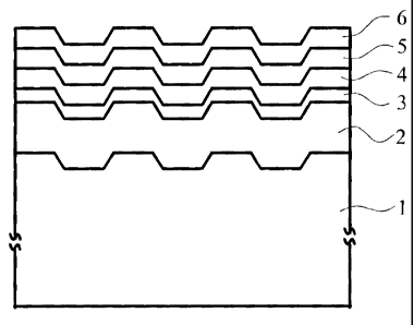
FIG. 1 is a structure diagram showing the rewritable optical recording
medium with Zn0 near-field optical interaction layer for disks in this
invention.
FIG. 2 shows the working principle of write-in, readout, and erasing marks
of a rewritable optical recording medium with Zn0 near-field optical
interaction
layer for disks in this invention.
FIG. 3 is a schematic illustration showing one preferred embodiment of the
pick-up head and optical lens of a disk driver in coordination with a
rewritable
optical recording medium with Zn0 near-field optical interaction layer for
disks
in this invention.
lU FIG. 4 shows the readout results of the recorded marks of the rewritable
optical disk with zinc-oxide (Zn0) near-field optical interaction layer by
using
an optical disk tester.
CA 02415650 2003-O1-07
4037 0004
Description of the Preferred Embodiments
The following descriptions of the preferred embodiments are provided to
understand the features and the structures of the present invention.
Figure1 is a structure diagram showing the rewritable optical recording
medium with zinc-oxide (Zn0) near-field optical interaction layer for disks
according to present invention. The structure of the rewritable optical
recording
medium comprises a transparent substrate 1 and a plurality of thin film layers
formed on said a transparent substrate 1. The plurality of thin films consist
of a
first transparent dielectric thin film layer 2, a zinc-oxide (Zn0) nano-
structured
thin film layer 3 that is capable of causing localized near-field optical
effect, a
second transparent dielectric thin film layer 4, a rewritable recording layer
5,
and a third transparent dielectric thin film layer 6. The transparent
substrate 1
is made of Si02 glass materials, or doped Si02 glass materials with
Sodium(Na), Lithium(Li), Caicium(Ca), Potassium(K), Aluminum(AI),
Germanium(Ge), Boron(B), etc. in various ratio, or transparent polymerized
materials which comprise polycarbonate, or epoxy resin, etc. The first
transparent dielectric thin film layer 2, the second transparent dielectric
thin
film layer 4 and the third transparent dielectric thin film layer 6 are
selected
from the group of the transparent dielectric materials consisting of ZnS-Si02,
ZnS-SiOX, Si02, SiOX, or SiNX. The first transparent dielectric thin film
layer 2,
the second transparent dielectric thin film layer 4 and said third transparent
dielectric thin film layer 6 are single or multiple layer structure. The
optimal
thickness of said first transparent dielectric thin film layer 2 is in the
range of
about 50nm to 300 nm. The optimal thickness of said second transparent
dielectric thin film layer 4 is in the range of about 5nm to 100nm. The
optimal
a
CA 02415650 2003-O1-07
4037 0004
thickness of said third transparent dielectric thin film layer 6 is in the
range of
about 5nm to 100 nm. The zinc-oxide (Zn0) nano-structured thin film layer 3
that is capable of causing localized near-field optical effect is made of
compound of zinc-oxide (Zn0), or the compositions of zinc-oxide and zinc. The
optimal thickness of said zinc-oxide (Zn0) nano-structured thin film layer 3
that
is capable of causing localized near-field optical effect is in the range of
about
5nm to 100nm. The rewritable recording thin film layer 5 is a rewritable
material of photo-thermal effect or magneto-optical effect. The material of
the
rewritable recording thin film layer 5 is selected from GeXSbYTeZ, InXSbyTeZ,
AgWInXSbyTeZ, FexTbyCoZ, GdXTbYFez or Co~Pty, doping with some elements
such as Copper(Cu), Zinc(Zn), Arsenic(As), Tin(Sn), Gold(Au), Mercury(Hg),
Thallium(TI), Lead(Pb), Bismuth(BI), Gallium(Ga), Germanium(Ge),
Cadmium(Cd), Indium(In), Antimony(Sb), Silver(Ag), Selenium(Se), and
Tellurium(Te). The rewritable recording thin film layer 5 is a single or
multiple
layer structure. The optimal thickness of the rewritable recording thin film
layer
5 is in the range of about 5nm to 100nm.
Figure 2 shows the working principle of the write-in, readout, and erasing
marks of a rewritable optical recording medium with Zn0 near-field optical
interaction layer for disks according to the present invention. The light
beams
(in/out) 7 of light source via the optical lens 9 of a pick-up head of disk
driver 8
penetrate the transparent substrate 1, and the first transparent dielectric
thin
film layer 2 thereto focusing on zinc-oxide (Zn0) nano-structured thin film
layer
3 that is capable of causing localized near-field optical effect. The
localized
near-field optical interaction beyond diffraction limit 10 generated by the
interaction of the focused laser and the rewritable recording layer 5 can
write
and read the storage data of said recorded marks with the size below the
9
CA 02415650 2003-O1-07
4037 0004
optical diffraction limit 11.
Therefore, accompanying with a rotating disk and a high-speed write-in
and readout scanning pick-up optical head of a disk driver, the writing and
reading action of ultrahigh density rewritable optical recording medium can be
carried out. The first transparent dielectric thin film layer 2 and the second
transparent dielectric thin-film layer 4 can protect and stabilize the zinc-
oxide
(Zn0) nano-structured thin film layer 3 that is capable of causing localized
near-field optical effect, and said second transparent dielectric thin-film
layer 4
maintains a fixed near-field distance between said rewritable recording layer
5
and said zinc-oxide (Zn0) nano-structured thin film layer 3 that is capable of
causing localized near-field optical effect. The third transparent dielectric
thin
film layer 6 can protect and stabilize the structure of the rewritable
recording
layer 5 to extend its lifetime.
As shown in Fig. 3, it is a preferred embodiment of a rewritable zinc-oxide
(Zn0) near-field optical disk 12 and pick-up head of disk driver 8. The
rewritable zinc-oxide (Zn0) near-field optical disk 12 rotates in the rotation
direction of optical disk 13, the tracking and focusing mechanism of the disk
driver maintains the pick-up head optical lens 9 and pick-up head of disk
driver
8 at the proper position to focus on the rewritable zinc-oxide (Zn0) near-
field
optical disk 12. The localized near-field optical interaction beyond
diffraction
limit 10 coupled between the zinc-oxide (Zn0) nano-structured thin film layer
3
and rewritable recording layer 5 can successfully write and read said the
recorded marks 11 with the size below the optical diffraction limit.
One of the experimental readout results of the rewritable zinc-oxide (Zn0)
near-field optical disk 12 is displayed in Fig. 4. A disk tester (manufactured
by
Pulstec Industrial Co., Ltd., Model DDU-1000) with the wavelength of light
io
CA 02415650 2003-O1-07
4037 0004
source at 673 nm and numerical aperture (NA) of the pick-up head lens at 0.6
is used to write-in and readout the pre-recorded 100 nm marks on a rewritable
zinc-oxide (Zn0) near-field optical disk 12 in this invention. The disk is
rotated in a constant liner velocity at 3.5 m/s, the write-in laser power out
of the
pick-up head is 14 mW, and the readout laser power out of the pick-up head is
5 mW. The readout results measured by a spectrum analyzer are shown in Fig.
4. The measured carrier-to-noise (CNR) value of the recorded 100 nm marks
is 33.23 dB. It is clearly evident that rewritable zinc-oxide (Zn0) near-field
optical disk 12 described in this invention is capable of write-in and readout
marks below the optical diffraction limit.
While this invention has been described in conjunction with particular
embodiments, it is evident that alternatives, modifications and variations
will
now be apparent to those skilled in the art. Accordingly, the present
invention
is intended to embrace all such alternatives, modifications and variations and
fall within the spirit and scope of the appended claims. Moreover, the
description and illustration of the invention is by way of example, and the
scope of the invention is not limited to the exact details shown or described
as well as the order of structure, the values, angles, directions of focusing
beams.
lr