Note: Descriptions are shown in the official language in which they were submitted.
CA 02415661 2004-11-29
1
A METHOD FOR PERFORMING WRITE AND READ OPERATIONS IN A
PASSIVE MATRIX MEMORY. AND APPARATUS FOR PERFORMING THE
METHOD
The present invention concerns a method for performing write and read
operations in a matrix addressed memory array of memory cells comprising an
electrically polarizable material exhibiting polarization remanence, in
particular
an electret or ferroelectric material, wherein a logical value stored in a
memory
cell is represented by an actual polarization state in the memory cell and is
determined by detecting a charge flow to or from the cell in response to the
application of voltages to the word and bit lines for addressing the memory
cells
of the array, wherein the charge flow detection in particular is based on
detecting a charge flow component caused by a change of polarization in said
polarizable material, and wherein write and read operations are performed
under
control of a control circuit device. The present invention also concerns an
apparatus for performing the method, said apparatus including at least one
matrix addressed memory array of memory cells comprising an electrically
polarizable material exhibiting polarization remanence, in particular a
ferroelectric material, wherein a logical value stored in a memory cell is
represented by the polarization state in individual, separately selectable
memory
cells and determined by detecting a charge flow to or from said memory cells
in
response to an application of voltages to the word and bit lines for
addressing
the memory cells of an array, said charge flow detection in particular being
based on a charge flow component caused by a change of polarization in said
polarizable material.
Memory devices based on ferroelectric thin films are presently approaching a
level of maturity where implementation in practical devices becomes possible.
Two main types of device architectures are of relevance, involving either
active
or passive matrix addressing of the stored data.
CA 021415661 2004-11-29
2
In active matrix-addressed architectures, each bit is stored in a memory cell
consisting of a ferroelectric-filled capacitor structure with an associated
dedicated microcircuit. The ferroelectric material is typically polarized in
one of
two stable states, representing a bit of information. The memory device
comprises a large number of such cells, arranged in a matrix of conductors.
Typically, the ferroelectric materials used in such devices are inorganic
ceramics, e.g. perovskites.
In passive matrix addressed architectures, which are the ones of primary
relevance in the present invention, the thin-film ferroelectric material is
sandwiched between two orthogonal sets of electrodes such that a capacitor
like
structure is formed in each overlap region between crossing electrodes. A bit
is
stored as a polarization state in the capacitor structure, which constitutes
an
elementary memory cell. No active circuitry is involved in connection with
each
cell, hence the term passive matrix addressing. This architecture is generally
dependent on ferroelectrics with particular hysteresis properties, and at
present
only a few, organic based ferroelectrics have been identified as potentially
useful
in practice. The information is typically read destructively, i.e. by imposing
an
electric field that causes polarization alignment in the memory cells along
the
reading field direction.
In many applications, it is desirable to perform read/write operations in a
given
memory cell a large number of times, in which case the polarizable material is
forced to undergo repeated polarization reversals and ultimately becomes
fatigued. Fatigue manifests itself in different ways, most prominently as
increased coercive field, lower remanent polarization and slower switching,
all of
which are highly undesirable in memory devices. Another phenomenon which
complicates the readout process is imprint. When a cell is left in the same
polarization state (i.e. logic state) for an extended time period, it may
develop a
tendency to be "frozen" into that state, such that the driving voltage must be
CA 02415661 2004-11-29
3
increased and/or applied for a longer time in order to dislodge it and switch
it to
the other polarization direction.
Prior art reading protocols that employ read pulses of fixed length must take
into
account the large spread in cell switching speeds and polarization response
that
develops due to fatigue and/or imprint. Thus the pulses must have a high
voltage and a long duration to be sure that the worst-case scenario could be
handled. This is undesirable for several reasons. A high voltage implies
higher
cost and more space-demanding driving circuitry, more power consumption and
increased cross-talk. Longer pulses imply lower data access and transfer
speeds. Finally, employing long pulses at high voltage even to cells that are
pristine or only moderately fatigued shall by itself contribute to accelerated
fatigue.
As concrete examples of relevant prior art concerning methods for readout of
data from a ferroelectric memory devices, reference can be made to EP patent
application No. 0 767 464 A2 (Tamura & al.) which in order to minimize
disturbance of the logic state of a ferroelectric memory cell, applies a pulse
voltage protocol which avoids large voltage excursions across the memory cell
and the readout voltage protocol is moreover static with respect to temporal
as
well as amplitude aspects of the voltage pulses to be applied. Reference can
further be made to US patent No. 5 487 0129 (Kuroda) which discloses the use
of a refreshing procedure after a certain number of read/write operations
applied
to a memory cell has been executed, said refreshing procedure consisting of
applying a polarization voltage Vp higher than the write voltage V0. This
ensures
to remove a fatigue induced reduction in the ferroelectric polarization and
restore a higher polarization value of the memory cell. However, such a
refreshing procedure will at best only be applicable in special instances,
e.g. in
the case where fatigue are due to charge accumulation and domain pinning
because of shallow charge traps, but would be of little help in more
complicated
cases where deep charge traps, vacancy migration or when an irreversible
CA 02415661 2004-11-29
4
chemistry at the electrodes are involved. It should moreover be noted that
both
the above mentioned publications relate to active matrix addressable memory
devices only, whereas it would be desirable that the write/read protocols
should
be applicable to passive matrix addressable memory devices as well.
It is a major object of the present invention to provide new methods for
reading
and writing data in memory devices based on electrically polarizable material,
in
particular ferroelectrics, whereby the polarization can be probed and
controlled
by methods that are less prone to create fatigue, yield faster data speeds and
are less demanding of the driving circuitry than present-day alternatives.
According to the present invention, there is provided a method for performing
write and read operations in a matrix addressed memory array of memory cells
comprising an electrically polarizable material exhibiting polarization
remanence,
wherein a logical value stored in a memory cell is represented by an actual
polarization state in the memory cell and determined by detecting a charge
flow
to or from said memory cell in response to the application of voltages to word
lines and bit lines for addressing the memory cells of the array, wherein the
charge flow detection in particular is based on detecting a charge flow
component caused by a change of polarization in said polarizable material, and
wherein write and read operations are performed under control of a control
circuit device, characterized by recording a dynamic charge response of one or
more of the memory cells during a read operation, limiting a degree of
polarization in the polarizable material during each read operation to a value
dependent on the recorded dynamic charge response and as defined by the
control circuit device, with said value ranging from greater than zero to an
upper
limit less than the saturation magnitude of the polarization and being
consistent
with predetermined criteria for a reliable detection of a logic state of a
memory
cell, and controlling the write and read operations according to an actual
instantaneous charge response information.
Preferably, the electrically polarizable material is an electret material.
CA 02415661 2004-11-29
Preferably, the electrically polarizable material is a ferroelectric material.
Preferably, the stored logical value of a memory cell is determined by an
application of one or more voltage pulses, the characteristics of which is
controlled by the control circuit device.
In that connection it is preferred to establish an addressing history for the
memory in terms of recorded exposure of the memory cells to fatigue and
imprint inducing factors and/or acquiring dynamic charge response information
from one or more reference cells or pairs of reference cells and/or one or
more
memory cells or pairs of memory cells in the matrix, and establishing the
predetermined detection criteria and/or the acquired charge response
information in order to adjust the characteristics of the voltage pulse or
pulses,
and the addressing history may then include the accumulated number of write
and/or read operations and/or imprinting time in specific memory cells or
groups
of specific memory cells, or dynamic charge response information can include
information about previously recorded charge response behaviour of the
memory cells. It is also then preferable that the dynamic charge response
information is acquired from at least one pair of reference cells in the
matrix, one
cell in each pair representing a logic 0 and the other a logic 1.
Preferably, the control circuit device performs continuous or periodic
analysis of
random and systematic noise contributions to the recorded dynamic charge
response from said reference cells or addressed memory cells, employing the
results from said analysis as input data into the algorithm for controlling
the
read/write protocol. It is then in addition also preferred that said analysis
of noise
contributions is based upon a statistical spread of dynamic charge responses
recorded from cells in known logic states, from single cells being addressed a
number of times and/or from a set of similar, but physically different memory
cells.
CA 02415661 2004-11-29
6
Preferably, in an embodiment of the method according to the invention wherein
the control criteria are based on dynamic charge response information, it is
advantageous that at least one of said voltage pulse or pulses is a step
voltage
pulse of variable length, said length being controlled by said circuit control
device and/or that said control circuit device records the plateau values
aSATURATION and 6BACKGROUND of the charge responses in cells
representing a logic "0" and a logic "1", respectively, at various points in
time
throughout the lifetime of the memory device, and/or that said control circuit
device generates a threshold value for decision on logic state in said memory
cells in said matrix, of magnitude 6TH=(aSATURATION + ~BACKGROUND)12:
and in another embodiment that the control circuit device employs charge
response information acquired from recording the dynamic charge response of a
group of memory cells selected at randomly chosen locations in the memory
array.
According to the present invention, there is also provided an apparatus for
performing write and read operations, said apparatus including at least one
matrix addressed memory array of memory cells comprising an electrically
polarizable material exhibiting polarization remanence, wherein a logical
value
stored in a memory cell is represented by the polarization state in
individual,
separately selectable memory cells and determined by detecting a charge flow
to or from said memory cells in response to an application of voltages to the
word and bit lines for addressing the memory cells of an array, said charge
flow
detection in particular being based on a charge flow component caused by a
change of polarization in said polarizable material, and wherein the apparatus
is
characterized in that it comprises circuitry for recording a dynamic charge
response of one or more memory cells during a read operation and adjusting
said application of voltages to limit a degree of polarization change in said
polarizable material during each read operation to a defined value, with said
value ranging from greater than zero to an upper limit less than the
saturation
magnitude of the polarization, and a circuit for controlling the write and
read
CA 02415661 2004-11-29
7
controlling the write and read operations to the memory cells, according to an
actual instantaneous charge response detected in a read operation.
Preferably, the memory array comprises reference cells with known logic
states,
and it is then preferable that the reference cells are localized in pairs, one
representing a logic "0" and the other a logic "1 ", or that the reference
cells are
distributed throughout the array.
Preferably, selected cells among said reference cells are assigned to track
the
fatigue and imprint development of specified groups of memory cells in said
array, by being exposed to the same pattern of polarization history and
switching
events, and then the groups of memory cells can be localized on one or more
word or bit lines in the array.
The invention shall now be explained in detail, with reference to the
accompanying drawing figures, in which
fig.1 a shows a general polarization hysteresis curve for a ferroelectric
material,
fig. 1 b schematically memory cells connected to word and bit lines in a
passive -
matrix configuration,
figs. 2a and 2b the step response time evolution at low and high temporal
resolution, respectively, of the polarization in test cells containing
ferroelectric
materials in pristine and in fatigued states, and
fig. 3 a schematic example of a circuit for reading of data from memory cells
according to the present invention.
In order to facilitate a better understanding of the present invention follows
below a brief description of the general background and the general physical
principles involved in the realization of the invention, before specific
examples of
embodiments thereof are given.
CA 02415661 2004-11-29
Fig. 1 a shows a general polarization curve defining the polarization response
of
a ferroelectric memory cell, i.e. its logic "0" or logic "1" state, and
provides the
background for the following discussion thereof.
With reference to fig. 1 a, it is assumed that the memory cell to be read
resides
initially in a quiescent state without an imposed electric field and that the
ferroelectric material in the cell is in a polarization state characterized by
either
position +PR or -PR along the polarization axis, depending on the logic state
assigned to the cell. According to prior art, a reading operation to ascertain
which of these states the cell is in shall involve the application of a
reading pulse
across the cell with a voltage +VSWITCH~ The latter voltage exceeds VC, the
voltage corresponding to the coercive field in the memory material, by a
margin
which is sufficient to drive the memory material into the saturation regime,
i.e.
into the region of the hysteresis curve that is closed and nearly linear. If
the cell
previously resided in the +PR state, only a small charge flows to/from the
cell,
leaving the cell in the +PR state as before. In fig.1a, this small charge flow
is
indicated by the quantity P". However, if the cell was initially residing in
the -PR
state, the polarization shall undergo a reversal with attendant significant
charge
transfer between the cell and the electrodes. In fig. 1a, this charge flow is
indicated by the quantity P*. Thus, by monitoring the amount of charge
transferred, the logic state of the cell is determined. Since this procedure
destroys the memory content of the cell, a separate pulse cycle must be
imposed on the same or another selected cell in the memory device, whereby
the logic state of that cell is set to the original (pre-read) value of the
cell that
was read.
Although the present invention has general applicability to all electrically
polarizable materials that exhibit hysteresis or remanence, the following
discussion shall for explicitness and simplicity refer to ferroelectric
materials
employed in passive matrix addressing architectures.
According to the present invention, the current flow to a given memory cell is
controlled in such a way that the polarization change during a read operation
is
CA 02415661 2004-11-29
9
less than the saturation polarization magnitude, but sufficient for a decision
to be
made about the logic state of the cell. Typically, a step voltage is applied
to the
memory cell in question, and the polarization response in the cell is
monitored
via the current transport to that cell. The voltage is turned off when either:
a) A certain charge accumulation time has elapsed, or
b) A certain accumulated charge has been detected.
This shall typically occur at a point in time where only a fraction of the
switchable
polarization has been switched. In this way, several advantages are realized:
- The ferroelectric material undergoes only partial polarization reversal,
leading to less fatigue.
- Since each reading event is only partially destructive, a given cell may
sustain several reads before restoration of data becomes necessary.
- An early decision can be made regarding logic state, speeding up the
reading process.
- Restoration of polarization loss due to read operations ("write-back")
requires much less charge transfer per bit read, regardless of whether
restoration is made after each read or after several reads.
A crucial element in the scheme described here is the correct choice of charge
accumulation time in the reading mode. For a given cell, this time shall
typically
increase as the cell becomes fatigued, and it becomes necessary to adjust the
read pulsing protocol accordingly. Either a predictive or a monitoring mode of
defining the accumulation time may be used.
In the former, the accumulation time is adjusted according to a program that
predicts the degree of fatigue from data on recorded use of the device. This
must include error margins to take into account all important parameters that
affect fatigue development, e.g. the temperature history, as well as cell-to-
cell
and device-to-device manufacturing tolerances.
In the latter, the evolution of the cell response (switching speed) is
monitored
throughout the lifetime of the device, and the results are used to adjust the
pulsing protocol, in particular the charge accumulation time. In a preferred
CA 02415661 2004-11-29
embodiment of the present invention, a self diagnostic scheme is included
where the condition and time evolution of the memory cells are monitored
continuously by reference cells that are subjected to environmental and
operational conditions that match closely those of the memory cells
themselves.
In the above description of the general background of the invention, it was
tacitly
assumed that the charge transfer is near complete within each read or write
operation, and the dynamic aspect of the read/write process was ignored.
Depending on the ferroelectric involved, the speed of polarization reversal
may
vary within wide limits, with inorganic ferroelectrics typically switching
several
10 orders of magnitude faster than the organic or polymer types. Prior art has
been
to a large extent centered on inorganic ferroelectrics, with primary emphasis
on
the total switching time, whereas the details of the switching transient have
received little or no attention in connection with possible exploitation in
read/write operations. With the advent of memory devices incorporating organic
and polymeric ferroelectrics which typically switch much slower than their
inorganic counterparts, the dynamic behaviour becomes an important factor
affecting the overall device speed. At the same time, the slower switching
provides opportunities for novel read/write schemes, since the time scales are
longer and it is easier to intervene during the transient phase.
In figs. 2a and 2b are shown the dynamic responses for memory cells containing
a polymeric ferroelectric. The cells were subjected to a step voltage VS = 20
V,
and the time evolution was recorded for the cumulative charge density ~, i.e.
charge transferred per unit area of interface between ferroelectric and
electrodes, after initiation of the step pulse. Two sets of curves are shown.
In the
first set, encompassing the upper three curves in each figure, the cell is
switched from a logic state "1" to a logic state "0", undergoing polarization
reversal with large transfer of charge. In the second set, encompassing the
closely grouped lower three curves in each figure, the cell already resided in
a
logic state "0" prior to the application of the step voltage, and only a small
dielectric displacement charge response was observed. Each set of curves
comprised cells that were either in a pristine state, i.e. without fatigue, or
had
CA 02415661 2004-11-29
11
been fatigued through 106 or 107 read/refresh operations involving complete
polarization reversal in each operation.
As can be seen, there is an initial current surge followed by an asymptotic
fall-off
in current towards zero, i.e. the charge density 6 increases rapidly from zero
and
reaches a plateau. The transient is much more rapid in the non-switching case
(i.e. logic state "0" -~ "0") than in the switching case (i.e. logic state "1"
-~ "0"),
and the asymptotic values for charge density a are lower in the former case
(BACKGROUND) than in the latter ('SATURATION). Fatigue manifests itself
as a lower plateau value aSATURATION (i.e. lower PR) and a slower transient,
and is clearly most prominent in the switching case. The time to reach 50% of
maximum polarization in a new cell is ~1 ps, but it can take 100 ps for a
fatigued
cell. According to the present invention, reading of data is performed by
applying
a voltage pulse, typically a voltage step, and detecting whether or not the
charge
density 6 exceeds a certain defined threshold at some point in time after the
pulse was initiated. This threshold shall not be reached, even after a long
delay,
if the cell is initially in a "0" logic state, but shall be exceeded if the
cell is initially
in a "1" logic state. In the latter case, the read pulse voltage across the
memory
cell is removed as soon as this level is reached.
This can be illustrated by the following example. Assume that the device in
question contains individual memory cells with characteristics as shown in
figures 2a and 2b. As can be seen, for a cell in the "0" state, the
accumulated
transferred charge rises rapidly (in less than 0.5 ~,s) to approx.
6BACKGROUND=2 p,C/cm2, from which point and onwards it stays virtually
unchanged. For a cell in the "1" state, however, the accumulated transferred
charge continues to rise rapidly after this point, reaching approx.
aSATURATION = 8.5 ~C/cm2 after approximately 8 ~,s in the case of a new cell.
For a fatigued cell, the rise is less rapid and the final value lower, but the
difference from a cell in the "0" state is clear.
CA 02415661 2004-11-29
12
As a discrimination criterion, one may prescribe that a cell shall be defined
as
being in a "1" state if a at some time ~TH after initiation of the read pulse
exceeds a certain threshold, e.g. 6 >_ 6TH = 7 NC/cm2. This threshold should
be
chosen to be well above the maximum value reached by cells initially in the
"0"
state, in this case 6BACKGROUND = 2 NC/cm2. From fig. 2b one observes that
the charge accumulation time ~TH to reach ~H from a "1" state shall be approx.
4 Ns for the pristine cell, 8 Ns for the cell fatigued 106 times and 80-100 Ns
for
the 10~ operations fatigued cell. According to prior art which relies on
complete
switching and a fixed charge accumulation time, the latter would have to be
defined sufficiently long to permit completion of the switching transient in
the
worst case, i.e. with fatigued cells. Thus, the read pulse would have to be
chosen in the range 50-100 ps rather than 1 irs. According to the present
invention, however, the read-out pulse is stopped when the accumulated charge
density reaches the threshold value crfH, and the logic state "1" is assigned
to
the cell. If this threshold is not reached during a certain defined time span
'~"'~TH~ the cell in question is in a logic state "0".
The above scheme implies that the read pulse is lengthened automatically as
the response of the cell is slowed down due to fatigue, always being kept as
short as possible and consistent with the defined threshold criterion. This
provides the following advantages:
- Firstly, there is a gain in reading speed over the prior art full switching
scheme.
- Secondly, if data are written back to the same cell, less polarization
reversal is involved, and the write-back operations can be shortened
commensurately with the read operation case. Imprint effects (i.e. the
tendency
for the ferroelectric material in the cell to lock into a logic state where it
has
resided for some time) may shorten the write-back time further, depending on
materials and operating conditions.
CA 02415661 2004-11-29
13
- Thirdly, since the polarization switching and electric field exposure is
minimized, fatigue shall generally progress much more slowly than in the full
switching scheme. Tests on device relevant polymeric ferroelectrics
demonstrated that dynamic readout according to the present invention increased
the fatigue resistance (i.e. the number of read/write-back operations with
acceptable confidence level) by several orders of magnitude compared to prior
art switching protocols employing full polarization reversal.
- Fourthly, multiple read operations between each write-back operation are
possible when agATURATION " aBACKGROUND~
Now a preferred embodiment, namely self-diagnostic determination of memory
cell response shall be discussed in more detail. As described above, the
charge
accumulation time must be increased as the cells fatigue. Ideally, each cell
in
the memory device should be read with a read pulse length optimally adjusted
for that cell. This is difficult, since the response characteristics shall
vary from
cell to cell due to manufacturing tolerances and fatigue/imprint history. The
latter
in particular may lead to very large cell-to-cell variations developing over
time,
since fatigue and imprint not only relates to the number of read/write
operations
experienced by the individual cells, but also to the combined effect of
voltage
stress (amplitude/polarity/duration) and other factors such as temperatures
experienced by the cell during its lifetime.
As a consequence, a predictive approach to read pulse adjustment shall
generally be relatively coarse, allowing for a spread in cell properties which
increases with time and use. Alternatively, one must allocate significant
resources in the device that are dedicated to keep track of the cumulative
fatigue on cells. This task may be simplified by protocols that distribute
wear
among the total number of memory cells in the device in such a way that cells
with comparable fatigue history can be identified in groups or blocks.
CA 02415661 2004-11-29
14
A monitoring, or self diagnostic approach shall in most cases be preferable.
The
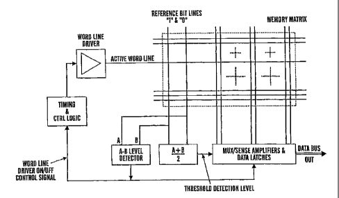
basic principle can be exemplified as follows, with reference to fig.3. For
each
row or cluster of memory cells one uses two reference cells, one polarized in
the
"1" state and the other in the "0" state. These two cells are exposed to
fatigue-
inducing influences, in particular polarization switching, which are
representative
of the row or cluster of memory cells they are assigned to. Two modes of read
operations employing the reference cells shall be specifically mentioned here:
i) Throughout the operative lifetime of the memory device, the reference
cells are used to track the development of 6SATURATION and
6gACKGROUND, from which the threshold value a~-H is defined, stored and
updated. In addition, the relevant charge accumulation time ~TH to reach 6TH
for cells in the state is established. During the readout operation signals
from the
memory cells are compared with the threshold level 6TH at time ~TH, and the
logic state of the cell is determined. In one class of embodiments under this
scheme, the median value is used as a threshold level, i.e. 6TH -
(aSATURATION + 6BACKGROUND)~2~
Since this mode implies driving the reference cells to saturation, they shall
typically be sampled periodically, either in a separate sample operation or in
a
read operation involving an extended read pulse.
ii) During each read operation, both the "0" and the "1" reference cells are
subjected to a reading pulse, and the respective charge densities 60(x) and
61 (~) transferred to each are monitored as a function of the time ~ elapsed
after
initiation of the read pulse. As can be seen from fig. 2, the difference
(60(x)-61 (~)) between the two increases with time, starting at zero and
ultimately
reaching a value (6SATURATION-6BACKGROUND)~ At some time ~TH this
difference has reached a certain level where it can be reliably detected in
the
presence of noise and cell-to-cell variability, at which time the read pulse
is
terminated and the sense amplifiers of the row or the cluster of memory cells
CA 02415661 2004-11-29
that are associated with these reference cells are read. The recorded values
60('~TH) and 61 (~TH) are available at this point as input parameters for the
logic
state determination process.
In both cases i) and ii) above, the read pulse length iTH increases
automatically
as the cells fatigue, at the same time being kept as short as is consistent
with
certain pre-defined detection and discrimination criteria. The latter may be
selected to meet different confidence levels according to the intended use of
the
device.
Cases i) and ii) provide different advantages and drawbacks which can be
10 stated as follows.
Case i
Advantage: Direct information is obtained about the development of the
parameters aSATURATION and agACKGROUND~
Drawback: A separate pulse cycle is required.
Case ii
Advantage: Can be implemented without separate pulse cycle (but the reference
cells must be in the correct logic states at the initiation of the read
operation)
and imposes representative pulsing fatigue on the reference cells.
Drawback: Requires circuitry capable of generating thresholding/discrimination
parameters in real time. In "single shot" usage, i.e. when the data in the
cluster
or row of cells in question are read only once or at long intervals, the
discrimination parameters derived in this mode shall reflect the full noise in
the
captured single sampling event.
The physical implementation of readout circuitry employing reference cells may
be achieved in many ways obvious to a skilled person. An apparatus comprising
a matrix addressable array of memory cells and capable of performing write and
CA 02415661 2004-11-29
16
read operations thereto in accordance with the method of the invention is
shown
in fig. 3. It should be understood that the apparatus in fig. 3 is although
prima
face rendered as a passive matrix addressable array is not limited thereto,
but
that the matrix addressable array of memory cells might just as well be based
on
active matrix addressing, i.e. provided with memory cells including a
switching
transistor. The basic scheme shown in Fig. 3 may be used in conjunction with
both types of operation modes i) and ii) discussed above. Here, reference
cells
are located on two dedicated vertical addressing lines ("bit lines"), one with
"0"
cells and the other with "1" cells. In a read operation, a horizontal line
("word
line") at a time is subjected to a reading pulse, and the charge flowing to
the
cells at the crossing points between the addressed horizontal line and the
crossing vertical lines is monitored by circuitry shown at the bottom of the
matrix.
Thus, the memory cells on each given horizontal line have associated with them
a reference cell pair on that same line.
More bit tines with reference cells may, of course, be added at intervals
throughout the whole memory matrix. In certain cases it may be advantageous
to employ single "1" or "0"reference bit lines rather than pairs, or reference
cells
may occupy less than the whole length of a bit line, even down to a single
cell.
The latter shall be the case when reference cells are located along word lines
rather than bit lines, which is a variant of the present invention.
The diagram as shown in fig. 3 indicates hard wiring between the reference bit
lines and the reference signal detectors. However, by multiplexing and signal
routing, reference bit tines may be defined at any location in the matrix.
Thus, it
shall in many cases be advantageous to establish reference cells in regions of
the memory matrix that have been subjected to fatigue and imprint during the
regular use of the memory device, with the possibility of moving from location
to
location in the matrix throughout the lifetime of the memory device. In this
way,
realistic data shall always be available for the readout decision process.
CA 02415661 2004-11-29
..
17
For simplicity, circuitry for writing data to the cells in the matrix is not
shown in
fig.3. Write back to preserve the destructively read data may be done
immediately after the read operation with a pulse of approximately the same
length as determined in the read operation, or it may be postponed until the
polarization level in the cell has reached a lower value as a consequence of
multiple reads. In the latter case, a longer write back pulse shall be
required.
In order to obtain reliable reference data, the number of reference cells in
the
memory device should evidently be sufficiently large to permit close mimicry
of
the usage pattern of the actual memory cells in question, with small
statistical
spread. However, a large allocation of real estate and dedicated circuitry to
reference cells shall compete with the other memory and processing functions
in
the device, and in practice a limited number of reference cells shall be
associated with a much larger number of memory cells, which may be in close
physical proximity to the reference cells (e.g. in a cluster), or may be
linked to a
set of memory cells that experience mutually similar kind of reading and
writing
exposure. The latter may be, e.g. a given sector in the memory device
comprising cells not necessarily in mutual physical proximity, or a row of
cells in
an addressing matrix where the whole row is read at a time.