Note: Descriptions are shown in the official language in which they were submitted.
CA 02415666 2003-O1-10
WO 02/05345 PCT/USO1/21851
UV LASER SYSTEM AND METHOD FOR
SINGLE PULSE SEVERING OF IC FUSES
Related Applications
[0001] This patent~application derives priority from U.S. Provisional
Application
No. 60/217,746, filed July 12, 2000.
Federally Sponsored Research or Development
[0002] Not applicable.
Technical Field
[0003] The present invention relates to a laser-based system or method for
severing
integrated circuit (IC) device fuses, and, in particular, to such a system or
method that
employs a single UV laser pulse to sever an IC fuse.
Background of the Invention
[0004] FIGS. 1, 2A, and 2B show repetitive electronic circuits 10 of an IC
device on a
wafer or workpiece 12 that are commonly fabricated in rows or columns to
include multiple
iterations of redundant circuit elements 14, such as spare rows 16 and columns
18 of
memory cells 20. With reference to FIGS. l, 2A, and 2B, circuits 10 are also
designed to
include particular laser severable circuit fuses or Iinks 22 between
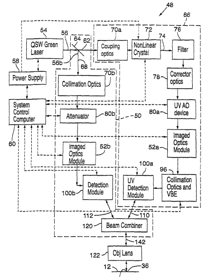
electrical contacts 24 that
can be removed to disconnect a defective memory cell 20, for example, and
substitute a
replacement redundant cell 26 in a memory device such as a DRAM, an SRAM, or
an
embedded memory. Similar techniques are also used to sever links to program
logic
products, gate arrays, or ASICs.
[0005] Links 22 are about 0.5-2 microns (,um) thick and are designed with
conventional
link widths 28 of about 0.8-2.5 ,um, link lengths 30, and element-to-element
pitches (center-
to-center spacings) 32 of about 2-8 ,um from adjacent circuit structures or
elements 34; such
as link structures 36. Although the most prevalent link materials have been
polysilicon and
1
CA 02415666 2003-O1-10
WO 02/05345 PCT/USO1/21851
like compositions, memory manufacturers have more recently adopted a variety
of more
conductive metallic link materials that may include, but are not limited to,
aluminum,
copper, gold nickel, titanium, tungsten, platinum, as well as other metals,
metal alloys,
metal nitrides such as titanium or tantalum nitride, metal silicides such as
tungsten silicide,
or other metal-like materials.
[0006] Traditional 1.047 ~,m or 1.064 ~,m infrared (IR) laser wavelengths have
been
employed for more than 20 years to explosively remove circuit Iinks 22. Before
link
processing is initiated, circuits 10, circuit elements 14, or cells 20 are
tested for defects, the
locations of which may be mapped into a database or program that determines
locations of
links 22 to be processed. Typically, the same IR laser beam used for
processing the links is
used, at reduced intensity, to locate the position of the focused spot of the
IR laser beam
with respect to reflective alignment marks, such as metal on oxide, positioned
at the corners
of the dies and/or wafers supporting the electronic components.
[0007] Conventional memory link processing systems focus a single pulse of IR
laser
output having a pulse width of about 4 to 20 nanoseconds (ns) at each link 22.
FIGS. 2A
and 2B show a laser spot 38 of spot size diameter 40 impinging a link
structure 36
composed of a polysilicon or metal link 22 positioned above a silicon
substrate 42 and
between component layers of a passivation layer stack including an overlying'
passivation
layer 44 (shown in FIG. 2A but not in FIG. 2B), which is typically 2000-10,000
angstrom
(~) thick, and an underlying passivation layer 46. Silicon substrate 42
absorbs a relatively
small proportional quantity of IR radiation, and conventional passivation
layers 44 and 46
such as silicon dioxide or silicon nitride are relatively transparent to IR
radiation. FIG. 2C
is a fragmentary cross-sectional side view of the link structure of FIG. 2B
after the link 22
is removed by the prior art laser pulse. The quality of the crater formed in
FIG. 2C is
neither uniform nor predictable.
[0008] To avoid damage to the substrate 42 while maintaining sufficient energy
to
process a metal or nonmetal link 22, Sun et al. in U.S. Pat. No. 5,265,114 and
U.S. Pat.
No. 5,473,624 proposed using a single 9 to 25 ns pulse at a longer laser
wavelength, such
as 1.3 ,um, to process memory links 22 on silicon wafers. At the 1.3 ,um laser
wavelength,
the absorption contrast between the Iink material and silicon substrate 20 is
much larger
than that at the traditional 1 ~,m laser wavelengths. The much wider laser
processing
2
CA 02415666 2003-O1-10
WO 02/05345 PCT/USO1/21851
window and better processing quality afforded by this technique has been used
in the
industry for several years with great success.
[0009] The 1.0 ~,m and 1.3 ,um laser wavelengths have disadvantages however.
In
general, the optical absorption of such IR laser beams 12 into a highly
electrically
conductive metallic link 22 is less than that of visible or UV beams; and the
practical
achievable spot size 38 of an IR laser beam for link severing is relatively
large and limits
the critical dimensions of link width 28, link length 30 between contacts 24,
and link pitch
32. This conventional laser link processing relies on heating, melting, and
evaporating link
22, and creating a mechanical stress build-up to explosively open overlying
passivation
layer 44.
[0010] The thermal-stress explosion behavior is also somewhat dependent on the
width
of link 22. As the link width becomes narrower than about 1 ~cm, the explosion
pattern of
passivation layers 44 becomes irregular and results in an inconsistent link
processing quality
that is unacceptable. Thus, the thermal-stress behavior limits the critical
dimensions of
links 22 and prevents greater circuit density.
[0011] U.S. Pat. No. 6,025,256 of Swenson et al. describes methods of using
ultraviolet (UV) laser output to expose links that "open" the overlying
passivation or resist
material with low laser power through a different mechanism for material
removal and
provide the benefit of a smaller beam spot size. The links are subsequently
etched.
[0012] U.S. Pat. No. 6,057,180 of Sun et al. describes methods of using UV
laser
output to remove links 22 positioned above a passivation layer of sufficient
height to
safeguard the underlying substrate from laser damage. This technique advocates
modification of the target material and structure well in advance of laser
processing.
[0013] Thus, improved. link processing methods are still desirable.
Summary of the Invention
[0014] An object of the present invention is, therefore, to provide a system
or method
that employs a single UV laser pulse to sever an IC fuse.
[0015] The present invention provides a Q-switched, diode-pumped, solid-state
(DPSS)
laser that employs harmonic generation through nonlinear crystals to generate
green and/or
IR and UV light. In a preferred embodiment, the type and geometry of the
nonlinear
crystals are selected to produce excellent beam quality suitable for
subsequent beam shaping
3
CA 02415666 2003-O1-10
WO 02/05345 PCT/USO1/21851
and focusing necessary to produce focused spot sizes that are advantageous for
severing of .
IC fuses. The temperatures of the nonlinear crystals may also be precisely
regulated using
temperature feedback control loops to maintain advantageous phase matching
conditions so
as to produce uniform processing laser pulse characteristics. In addition,
beam shape
quality may also be enhanced by an imaged optics module capable of spatially
filtering
unwanted beam artifacts.
[0016] In a further preferred embodiment, because many standard alignment
targets are
difficult to detect with a UV laser beam, a fraction of the green or IR output
may be
utilized for the separate purpose of target alignment. The fractional green or
IR target
alignment beam follows a separate optical path with a separate set of optical
element and is
attenuated to the proper power level. An imaged optics module for the
fractional green or
IR beam optimizes its shape for alignment scans. The green or IR alignment
beam and the
UV alignment beam pass through detection system modules and are separately
aligned to a
calibration target through a beam combiner common to both optical paths and
their
respective resulting reflected light is detected to calibrate the alignment
beam with the UV
link processing beam. The green or IR alignment beam can then be used to align
the
beams) to a given die, and the desired links on the die can be severed by the
UV link
processing beam without further calibration.
[0017] This invention provides the capability to produce high quality, focused
spots that
are smaller than conventionally used by IR link processing systems. The
invention also
provides improved UV pulse-to-pulse energy level stability while providing a
means to
deliver pulses at high repetition rates desired for improved throughput. This
invention
further provides a solution to the problem of aligning to alignment marks that
have little
contrast at the UV wavelength by using the green beam and/or IR beam,
generated by the
same source, as an alignment beam.
[0018] Additional objects and advantages of the invention will be apparent
from the
following detailed description of preferred embodiments thereof, which
proceeds with
reference to the accompanying drawings.
Brief Description of the Drawings
[0019] FIG. 1 is a schematic diagram of a portion of a DRAM showing the
redundant
layout of and programmable links in a spare row of generic circuit cells.
4
CA 02415666 2003-O1-10
WO 02/05345 PCT/USO1/21851
[0020] FIG. 2A is a fragmentary cross-sectional side view of a conventional,
large
semiconductor link structure receiving a laser pulse.
[0021] FIG. 2B is a fragmentary top view of the link structure and the laser
pulse of
FIG. 2A, together with an adjacent circuit structure.
[0022] FIG. 2C is a fragmentary cross-sectional side view of the link
structure of FIG.
2B after the link is removed by the laser pulse.
[0023] FIG. 3 is a schematic diagram of an embodiment of a laser system of the
present
invention including one or more alignment detection modules.
[0024] FIG. 4 is a simplified partly schematic view of portions of the laser
system of
the present invention including details of one embodiment of an imaged optics
module.
[0025] FIG. 5 is a table presenting parameters for preferred types of
nonlinear crystals.
[0026] FIG. 6 is a simplified schematic view of a detection module.
Detailed Description of Preferred Embodiments
[0027] FIG. 3 shows certain components of a preferred embodiment of laser
system 48
of the present invention and includes a secondary target alignment system 50.
FIG. 4
shows certain additional or optional components of laser system 48 together
with certain
components of one embodiment of an imaged optics module 52 and with the
secondary
target alignment system (STAS) 50 optionally omitted. Also for convenience in
FIG. 3, the
beam paths are shown with solid line arrows, and the electrical or signal
paths are shown
with broken line arrows. Although most of the broken line arrows are shown
pointing in
both directions for convenience, skilled persons will appreciate that many of
these signal
paths can be implemented as open loops.
[0028] With reference to FIGS. 3 and 4, a preferred embodiment of a laser
system 48
of the present invention includes a laser 54 that in general preferably
provides a wavelength
component that is shorter than 575 nm such as within a wavelength range of
about 510-575
nm, which may hexein after be referred to as green for convenience. However, a
longer
wavelength component within the IR region, preferably shorter than 1150 nm and
more
preferably within the range of 1020-1150 nm, may additionally be provided such
that the
longer wavelength is the first harmonic and the shorter (green) wavelength is
the second
harmonic. Laser 54 preferably includes a Q-switched, diode-pumped (DP), solid-
state (SS)
laser that preferably includes a solid-state lasant such as Nd: YAG, Nd: YLF,
Nd: YAP, or
CA 02415666 2003-O1-10
WO 02/05345 PCT/USO1/21851
most preferably Nd:YV04, that produces infrared light which is subsequently
converted to
green light via the nonlinear optical process of second harmonic generation.
Such lasers 54
may provide harmonically generated laser pulses or output 56 with a wavelength
component
such as about 532 nm (frequency doubled Nd:YVO~) or about 524 nm (frequency
doubled
Nd:YLF) with primarily a TEMoo spatial mode profile. A power supply 58
provides the
electrical power, RF power, and control signals to laser 54 and may be
controlled by a
system control computer 60.
[0029] Although Gaussian is used to describe the irradiance profile of laser
output 56,
skilled persons will appreciate that most lasers 54 do not emit perfect
Gaussian output 56
having a value of MZ=1. For convenience, the term Gaussian is used herein to
include
profiles where M2 is less than or equal to about 1.5, even though M2 values of
less than 1.3
or 1.2 are preferred. Skilled persons will appreciate that other wavelengths
are available
from the other listed lasants. Although laser cavity arrangements, harmonic
generation,
and Q-switch operation are all well known to persons skilled in the art,
certain details of
preferred embodiments will be presented herein.
[0030] Laser output 56 may optionally be passed through a variety of well-
known
expansion and/or collimation optics and propagates along a first optical path
62. When
secondary target alignment system (STAS) 50 is employed, laser output 56 meets
a
beamsplitter 64 that transmits a major portion of the energy of laser output
56 through a
UV target severing and alignment system (UV SAS) 66 along the first optical
path 62 and
deflects a fractional portion of the energy of laser output 56 through a STAS
50 along a
second optical path 68.
[0031] The majority of laser output 56 traveling along the first optical path
62 is
optically coupled, through collimation or coupling optics 70a, into a
nonlinear crystal 72 to
convert the first wavelength components) into UV light by the process of
harmonic
conversion. If, for example, laser output 56 contains generally only green
light such as
second harmonic light with a wavelength component at about 532 nm, then
nonlinear
crystal 72 provides wavelength converted output 74 such as fourth harmonic
light at with a
wavelength component at about 266 nm (frequency quadrupled Nd:YVOa). Persons
skilled
in the art will recognize that the process of fourth harmonic conversion is
not reliant on IR
content in laser output 56. Skilled persons will also appreciate that for
conversion to the
6
WO 02/05345 PCT/USO1/21851
[
CA 02415666 2003-O1-10
WO 02/05345 PCT/USO1/21851
third harmonic both green and IR light will be provided by Iaser 54 and passed
by
beamsplitter 64 such that nonlinear crystal 72 provides wavelength converted
output 74
with a wavelength component at about 355 nm (frequency tripled Nd:YVOa).
Skilled
persons will appreciate that many other wavelengths for output 74 are possible
depending
on the original wavelengths) propagated by laser 54 and the number of
nonlinear crystals
72. Skilled persons will also appreciate that in embodiments where the
preferred lasers 54
employ harmonic conversion, nonlinear crystal 72 is the "second" nonlinear
crystal and
preferably produces fourth or third harmonic conversion as described above.
Skilled
person will further appreciate an additional nonlinear crystal may be employed
to convert
first and fourth harmonic wavelength light to a fifth harmonic wavelength such
as 213 nm
(frequency quintupled Nd:YVOa).
[0032] Preferably, the geometry and type of at least the second nonlinear
crystal 72 are
chosen to produce excellent beam quality suitable for subsequent beam shaping
and
focusing necessary to produce focused spot sizes that are advantageous for
severing of IC
fuses or links 22. The geometry and type of this second nonlinear crystal 72
are
simultaneously selected to provide adequate energy per pulse output suitable
for severing IC
fuses. In particular, the length of nonlinear crystal 72 positioned along the
optical path is
chosen to balance the effects of the combination of the acceptance angle and
birefringence
walk-off, which may cause diminishment of beam quality with increasing crystal
length,
and pulse energy output that typically increases with increasing crystal
length. The length
of nonlinear crystal 72 positioned along the first optical path 62 is greater
than or equal to
about 1 mm and less than about 20 mm. Preferably, the length of nonlinear
crystal 72
positioned along the first optical path 62 is greater than or equal to about 3
mm and less
than or equal to about 12 mm. More preferably, the length of nonlinear crystal
72
positioned along the first optical path 62 is greater than or equal to about 4
mm and less
than or equal to about 8 mm. Most preferably, the length of nonlinear crystal
72 positioned
along first optical path 62 is greater than or equal to about 6 mm and less
than or equal to
about 8 mm. Conventional CLBO nonlinear crystals are, for example, 12-15 mm in
length
along the axis of propagation to maximize the amount of laser light
conversion. Positioning
a shorter length of nonlinear crystal 72, such as less than about 7 mm, along
the first
optical path 62 is particularly desirable for fourth and fifth harmonic
generation
7
CA 02415666 2003-O1-10
WO 02/05345 PCT/USO1/21851
applications. Furthermore, skilled persons will appreciate that although the
length of
nonlinear crystal 72 positioned along the first optical path 62 is preferably
collinear or
parallel with the major axis of nonlinear crystal 72, nonlinear crystal 72 may
be positioned
such that its surfaces or axes are neither parallel with nor perpendicular to
the first optical
path 62 travelling through the nonlinear crystal 72. Although a conventionally
large
nonlinear crystal can be employed for third harmonic applications, such a
crystal can also
be employed for fourth or fifth harmonic applications where the first optical
path 62 passes
through only a short length, less than about 7-10 mm, of the crystal.
[0033] Depending on the type of nonlinear crystal 72 employed, the geometry of
nonlinear crystal 72 may also be selected such that the dimensions transverse
to the
direction of beam propagation are chosen to be more generous than typically
required
strictly based on clear aperture considerations as routinely practiced by
those skilled in the
art. This transverse geometrical consideration provides for potential
hygroscopic
diminishment of the clear aperture and thereby maintains a sufficient area of
the overall
clear aperture during the useful life of nonlinear crystal 72. The other
sides, i.e. height and
width, of the nonlinear crystal 72 are typically 3-5 mm but may be larger, and
the entire
nonlinear crystal 72 is typically square or rectangular, but may be formed in
other shapes
as well.
[0034] Nonlinear crystal 72 is preferably fabricated from j3-BaBaOa. (barium
borate or
BBO), LiBsOs (lithium borate or LBO), or CsLiB60~o (CLBO). BBO, LBO, and CLBO
are
all preferred for converting laser output 56 into the near UV (third harmonic
generation),
with LBO being most preferred. BBO and CLBO are both preferred for converting
laser
output 56 into the UV fourth harmonic or fifth harmonic generation, with CLBO
being
most preferred. LBO is preferred for second harmonic generation, but many
other
nonlinear crystals are known to skilled persons and could be employed. Skilled
persons
will appreciate that different harmonics may employ different cuts of
nonlinear crystals 72
with respect to their crystallographic axes and different wavelength-dependent
coatings.
FIG. 5 is a table presenting parameters, including the lengths, for preferred
types of
nonlinear crystals. In FIG. 5, THG represents third harmonic generation; FHG
represents
fourth harmonic generation; FiHG represents fifth harmonic generation; PM
represents
phase-matching angle and may refer to crystal cut; and deff(pm/V) is a figure
of merit
CA 02415666 2003-O1-10
WO 02/05345 PCT/USO1/21851
representing the efficiency with which a nonlinear crystal is capable of
converting
fundamental wavelength light into higher harmonic light output.
[0035] In one particular embodiment, a BBO or CLBO nonlinear crystal 72 is
employed
to convert 532 nm laser output 56 into wavelength converted output 74 at about
266 nm
laser light through the process of fourth harmonic conversion. A BBO nonlinear
crystal 72
provides excellent conversion efficiency, maintains good beam quality in both
the vertical
and horizontal alignment axes, has a very good UV damage threshold, and is not
as
hygroscopic as some other common nonlinear crystals. BBO also has very good
transmission at 266 nm. CLBO is, however, preferred even though it is more
hygroscopic
than BBO because CLBO offers a better acceptance angle and smaller walk off
angle than
BBO.
[0036 The temperatures of the nonlinear crystals 72 are precisely regulated,
preferably
using temperature feedback control loops, to maintain advantageous phase
matching
conditions so as to produce uniform processing laser pulse characteristics at
the appropriate
wavelengths. In particular, laser output alignment is sensitive to changes in
the temperature
of the nonlinear crystals 72, such that both beam position, quality, shape,
and output power
can be significantly affected by small temperature changes in the nonlinear
crystals 72. A
module containing nonlinear crystal 72 may receive its power for temperature
regulation
from power supply S8. The desired temperature may be preset and/or controlled
directly
or indirectly from system control computer 60 or a subprocessor. The
temperature
regulation improves both alignment and target processing and also helps to
minimize
collateral damage to nontarget areas.
[0037] Wavelength converted output 74 is then passed through a wavelength-
selective
filter 76 to block any unconverted output emitted from nonlinear crystal 72
from being
further transmitted towards the subsequent components of UV SAS 66 and
ultimately the
workpiece 12. Although filter 76 could be omitted for applications where a
small degree of
unconverted output may be of little significance to downstream components or a
the link
severance performance with respect to particular materials, filter 76 is
preferably employed
to block green and/or IR light from interacting with link structures 36 and
from interfering
with operation of UV detection module 100a. If filter 76 is omitted,
downstream mirrors
9
CA 02415666 2003-O1-10
WO 02/05345 PCT/USO1/21851
may be coated to preferably reflect UV light and transmit or dump the green
and/or IR
Iight.
[0038] In the preferred embodiment, wavelength converted output 74 is then
transmitted
through a set of corrector optics 78 which deliver a substantially round beam
to an acousto
optic modulator (AOM) 80a. In this preferred embodiment which is shown in FIG.
3, the
laser output 56 is not modulated by a separate AOM, and AOM 80a is an
ultraviolet AOM
that follows corrector optics 76 to provide a more stable wavelength converted
output 74
from nonlinear crystal 72. AOM 80a is used to transmit only the desired laser
pulses of the
wavelength converted output 74 to the work surface and attenuate the energy of
desired
individual pulses to a desired pulse energy value for either IC fuse severing
or alignment
scans. AOM 80a is capable of switching between a high attenuation state to
provide laser
output power suitable for target alignment and a low attenuation state
suitable for link
processing. AOM 80a is also capable of completely blocking transmission of
wavelength
converted output 80a, particularly in a link processing autopulse mode. AOM
80a is
further selected to transmit desired laser pulses without adversely affecting
transmitted
beam quality. UV grade AOMs 80a suitable for this application are commercially
available. AOM 80a may be an electro-optic modulator (such as a Pockets cell)
instead of
an acousto-optic modulator. Alternatively, a polarization rotation element,
such as a half
wave plate or a liquid crystal cell, followed by a polarizer could be
employed. AOMs 80a,
their substitutes, and their uses are well known to persons skilled in the
laser art.
[0039] Despite the substantially round profile of wavelength converted output
74 at this
stage, there may be residual astigmatism or elliptical or other shape
characteristics that are
undesirable for an IC fuse severing process. Improved beam shape quality can
be achieved
with an optional imaged optics module 52a (generically 52) whereby unwanted
beam
artifacts axe filtered spatially. For convenience, image optics module 52
shown in FIG. 4 is
designated in FIG. 3 with 52a in UV SAS 66 and is designated with 52b in STAS
50.
[0040] Image optics module 52 preferably includes an optical element 90, a
lens 92, and
an aperture mask 94 placed at or near the beam waist created by the optical
element 90 to
block any undesirable side lobes and peripheral portions of the beam. In a
preferred
embodiment, optical element 90 is a focusing lens, and lens 92 is a
collimating lens to add
flexibility to the configuration of laser system 48. Varying the size of the
aperture can
CA 02415666 2003-O1-10
WO 02/05345 PCT/USO1/21851
control the edge sharpness of the spot profile to produce a smaller, sharper-
edged intensity
profile that should enhance the alignment accuracy. In addition, with this
arrangement, the
shape of the aperture can be precisely circular or also be changed to
rectangular, elliptical,
or other noncircular shapes that can be aligned parallel or perpendicular to
the link length
30. The aperture of mask 94 may optionally be flared outwardly at its light
exiting side.
(0041] In imaged optics module 52a, mask 94 may comprise a UV reflective or UV
absorptive material, but is preferably made from a dielectric material such as
UV grade
fused silica or sapphire coated with a multilayer highly UV reflective coating
other UV
resistant coating. Skilled persons will appreciate that aperture mask 94 can
be used without
optical elements 90 and 92.
[0042] In an alternative preferred embodiment, optical element 90 includes one
or more
beam shaping components that convert laser pulses having a raw Gaussian
irradiance profile
into shaped (and focused) pulses that have a near-uniform "top hat" profile,
or particularly
a super-Gaussian irradiance profile, in proximity to an aperture mask 94
downstream of
optical element 90. Such beam shaping components may include aspheric optics
or
diffractive optics. In this embodiment, lens 92 comprises imaging optics
useful for
controlling beam size and divergence. Skilled persons will appreciate that a
single imaging
lens component or multiple lens components could be employed. Skilled persons
will also
appreciate that shaped laser output can be employed without using an aperture
mask 94.
[0043] In one preferred embodiment the beam shaping components include a
diffractive optic element (DOE) that can perform complex beam shaping with
high
efficiency and accuracy. The beam shaping components not only transforms the
Gaussian
irradiance profile to a near-uniform irradiance profile, but they also focus
the shaped output
to a determinable or specified spot size. Although a single element DOE is
preferred,
skilled persons will appreciate that the DOE may include multiple separate
elements such as
the phase plate and transform elements disclosed in U.S. Pat. No. 5,864,430 of
Dickey et
al. , which also discloses techniques for designing DOEs for the purpose of
beam shaping.
The shaping and imaging techniques discussed above are described in detail in
International
Publication No. WO 00/73103 published on December 7, 2000. The relevant
portions of
the disclosure of corresponding U.S. Patent Application No. 09/580,396 of
Dunsky et al.,
filed May 26, 2000 are herein incorporated by reference.
11
CA 02415666 2003-O1-10
WO 02/05345 PCT/USO1/21851
[0044] In general, any of the preferred embodiments could be employed for link
severing. Although some of the embodiments offer substantial cost advantages,
the flat top
irradiance profile for wavelength converted output 74 achievable by shaping
and imaging
might be useful for preventing substrate damage at the center of the spot for
certain
varieties of link structure 36, particularly where the passivation layer 46
underlying the link
22 is particularly thin and sensitive to UV damage. The imaged shaped output
can create a
more uniform crater because the uniform shape of wavelength converted output
virtually
eliminates the possibility of creating a hot spot at the center. Imaged
shaping may therefore
facilitate the formation of craters with a very flat and uniform bottom in
addition to very
precisely shaped geometries and crisp edges.
[0045] Moreover, a high fraction of the beam energy can be delivered to
workpiece 12
without a large difference in fluence between the center and edges of the
imaged spot. In
addition, the flat top irradiance pxofile may be desired to maximize the
energy per pulse
that propagates through aperture mask 94 and therefore minimize the energy
clipped or
wasted by the size limit of the aperture. This approach may be of particular
use for UV
applications where the power of wavelength converted output 74 is low.
[0046] Skilled persons will also appreciate that the techniques described
herein also
permit enhanced repeatability and alignment accuracy. Because the dimensions
and
positions of the processed craters can be accurately predicted, such as in the
center of links
22, and can be made to have a narrower profile than conventional link severing
craters,
these techniques may be useful for increasing the circuit density of the
electronic
workpieces 12.
[0047] With reference again to FIG. 3, wavelength converted output 74
preferably
travels through a variable beam expander (VBE) 96 to allow a user to control
the spot size
of the beam. VBE 96 is positioned downstream of AOM ~Oa and preferably
downstream of
imaged optics module 52a, if it is employed. In a preferred embodiment, VBE 96
is
motorized and allows individual lens elements to be commanded by the system
control
computer 60 to move to programmed positions, thus enabling computer control
of.the
focused (shaped) spot size at the work surface. In a preferred arrangement, a
pair of
rotatable plates of glass to make small translational adjustments to the beam
may
additionally be employed. The rotatable plates are preferably positioned
between VBE 96
12
CA 02415666 2003-O1-10
WO 02/05345 PCT/USO1/21851
and detection module 100a, but can alternatively be positioned between
detection module
100a and beam combiner 120. The alignment adjustments for these plates can be
manually
performed, or their positions can be remotely controlled by the system control
computer
60.
[0048] Continuing through UV SAS 66, wavelength converted output 74 is
preferably
directed through a UV detection module 100a. FIG. 6 is a simplified schematic
view of a
preferred detection module 100 (generic for detection modules 100a and 100b).
For
convenience, the detection module 100 shown in FIG. 6 is designated, in FIG.
3, with 100a
in UV SAS 66 and with 100b in STAS 50.
[0049] Detection module 100 preferably includes a beamsplitter 102 that splits
off a
fraction of the incident wavelength converted output 74 so that it can be
sampled. This
incident beam may be split again, as desired, so that different types of
sensors 104 can
sample it. Preferably, detection module 100 includes a sensor 104 that is used
to measure
the incident beam during an alignment operation. Also in particular, detection
module 100a
preferably includes a sensor 104(a) that can characterize the pulsed output
characteristics
that axe important for a severing operation. Turn mirrors are used to direct
the incident
beam onto sensors 104, through attenuators 106 and focusing lenses 108 as
needed.
Beamsplitter 102 preferably passes the major portion of wavelength converted
output 74
along beam path 110a, shown in FIG. 4 and generically represented as beam path
110 in
FIG. 3.
[0050] Beamsplitter 102 of detection module 100 is also preferably used to
direct light
that is reflected from the work surface to a reflection sensor 114. The
reflected light is
designated as beam path 110b in FIG. 6 for convenience, and is generically
represented by
beam path 110 in FIG. 3. Reflection sensor I14 measures the reflected beam
during an
alignment operation. Turn mirrors axe used to direct the incident beam onto
sensors 114,
through attenuators 116 and focusing lenses 118 as needed. Sensor electronics
for sensors
104 and 114 preferably communicate with system control computer 60.
[0051] The maj or portion of wavelength converted output 74 is then preferably
directed
through a beam combiner 120 if STAB 50 is employed. Beam combiner 120
preferably
employs a dichroic mirror and directs wavelength converted output 74 through
objective
Lens 122 toward a desired laser target position 124 on the workpiece 12.
Skilled persons
13
CA 02415666 2003-O1-10
WO 02/05345 PCT/USO1/21851
will appreciate that other implementations of beam combiner 120 are possible.
Objective
lens 122 can also be referred to as a "second imaging," focusing, cutting, or
scan lens. A
variety of positioning systems that move the workpiece 12 and/or objective
lens and/or
beam 142 are known to skilled practitioners and could be employed. A Model
9800
positioning system made by Electro Scientific Industries, Inc. of Portland,
Oregon can be
modified to implement a preferred embodiment of the invention.
[0052] Preferably, the laser control system 60 directs the movement of
components of a
beam positioning system 130 and preferably synchronizes the firing of laser 54
to the
motion of the components of beam positioning system 130 such as described in
U.S. Pat.
No. 6,172,325 ('325 Patent) of Baird et al., which describes laser processing
power output
stabilization techniques employing processing position feedback that improve
pulse to pulse
peak energy level stability while providing a means to deliver pulses at high
repetition
rates.
[0053] During a link processing operation, a Q-switched solid state laser 54
operates in
cooperation with a pulse processing control system that employs an autopulse
mode and a
pulse-on-position mode to stabilize the pulse-to-pulse laser energy delivered
to target
locations on a workpiece 12 that is moved by beam positioning system 130. In
the
autopulse mode, laser pulses are emitted at a near maximum PRF, but the pulses
are
blocked from reaching the workpiece 12 by AOM 80a or an additional AOM within
laser
54 or along the first optical path 62. In the pulse-on-position mode, the
laser 54 emits a
pulse each time the positioning system 130 moves a workpiece location through
coordinates
that coincide with a commanded laser beam coordinate. The processing control
system
moves the positioning system 130 at a near constant velocity that causes
triggering of the
laser 54 at about the maximum PRF in response to the workpiece 12 passing
through a
regularly spaced apart set of commanded laser beam coordinates. The pulse
processing
control system sets the AOM 80a to a transmissive state whenever a location to
be
processed is commanded and sets the AOM 80a to a blocking state whenever a
location not
to be processed is commanded. The pulse-to-pulse energy level stability of
laser system 48
directly depends on the pulse-to-pulse energy level stability of laser 54. To
meet this
requirement, the interpulse period between emitted laser pulses is made
substantially equal,
thereby stabilizing its pulse-to-pulse energy level at the near maximum PRF.
This pulse-to-
14
CA 02415666 2003-O1-10
WO 02/05345 PCT/USO1/21851
pulse energy level stability reduces thermal and radiant effects that would
otherwise be
caused by laser duty cycle variations arising from firing IR laser at varying
interpulse
periods. Such thermal and radiant effects can include changes to the
refractive indices of
nonlinear crystals 72, thereby modifying the phase-matching conditions for
harmonic
generation, which causes Iarge variations in the harmonic output energy. Such
thermal and
radiant effects can also cause the energy per pulse of laser 54 to vary which
will then cause
the output of laser system 48 to fluctuate.
[0054] For link processing, laser system 48 is capable of producing laser
system output
140 having preferred parameters of link processing windows that may include
programmable energy per pulse values in a range of about 0.01 ~,J to about 10
~,J; spot size
diameters or spatial major axes of about 0.3 ,um to about 10 ~cm, and
preferably from about
0.5-5.0 ~,m, and most preferably less than 2 ~,m; and a pulse repetition
frequency (PRF) of
greater than about 1 kHz, preferably greater than about 20 kHz or even as high
as or higher
than 100 kHz; an ultraviolet wavelength, preferably between about 180-390 nm;
and
temporal pulse widths that are shorter than about 100 ns, and preferably from
about 4-20 ns
or shorter. The preferred Iink processing parameters of laser system output
140 are
selected in an attempt to circumvent damage to the underlying substrate 42 or
surrounding
structures 36.
[0055] When employing IJV SAS 66 for target alignment, AOM 80a is used to
attenuate wavelength converted output 74 to produce laser system output 140
having
preferred parameters that may include spot size and pulse width parameters
similar to those
used for link severing. The attenuated pulses of wavelength converted output
74 are
preferably generated at a PRF of about 20-100 kHz and have an output power of
about 0.01
mW to about I mW. Typically the attenuated pulses have less than 5 % of the
energy of the
link severing pulses for a given target alignment structure, but numerous
factors including
the reflectivity and other characteristics of the materials in these
structures or link structures
36 will determine the best process windows for severing pulses and for
alignment pulses for
the particular target.
[0056] With reference again to FIG. 3, laser output 56, beam splitter 64, and
second
optical path 68, when a STAS 50 is employed, the deflected Iower irradiance
portion of
Iaser output 56, laser output 56b, travels along the second optical path 68
and preferably
CA 02415666 2003-O1-10
WO 02/05345 PCT/USO1/21851
passes through expansion and/or collirnation optics 70b. Laser output 56b
preferably
contains green or IR light having an optical profile preferably optimized for
purpose of
target alignment.
[0057] Laser output S6b is then preferably directed through an attenuator 80b
that is
used to control the power of laser output 56b used for alignment scans.
Attenuator 80b is
preferably also used to stop laser output 56b from being transmitted to a
target during UV
alignment scans or UV link processing. Attenuator 80b may be the same or
different type
of device used for AOM 80a, but is preferably adapted for use with green
and/or IR laser
light. Attenuators 80b suitable for this application at these wavelengths are
also
commercially available. Attenuator 80b may alternatively be any one of the
many types of
laser shutters known to skilled practitioners.
[0058] Laser output 56b may optionally be passed through an imaged optics
module 52b
to optimize accuracy in the alignment process. Imaged optics module 52b may
include the
same or different components than imaged optics module 52a, but is preferably
adapted for
use with green and/or IR laser light. For example, image optics module 52b may
not
include a beam shaping element while imaged optics module 52a does include
one. In
addition, it may be desirable to have an aperture of a different shape and/or
size in the
aperture mask 94 in module 52b than those of the aperture mask 94 in module
52a. In a
preferred embodiment, laser system 48 includes both an imaged optics module
52a and an
imaged optics module 52b, and both imaged optics modules include a focusing
lens and an
aperture mask 94.
[0059] Laser output 56b is then directed toward a secondary detection module
100b,
which is similar to detection module 100a, but secondary detection module 100b
is adapted
for use with green and/or IR laser light. Detection module 100b preferably
includes a
beamsplitter 102 that splits off a fraction of the incident laser output 56b
so that it can be
sampled. This incident beam may be split again, as desired, so that different
types of
sensors 104 can sample it. Preferably, detection module 100 includes a sensor
104 that is
used to measure the incident beam during an alignment operation. Turn mirrors
are used to
direct the incident beam onto sensors 104, through attenuators 106 and
focusing lenses 108
as needed. Beamsplitter 102 preferably passes a portion of laser output 56b
along beam
path 112a, shown in FIG. 6 and generically represented as beam path 112 in
FIG. 3.
16
CA 02415666 2003-O1-10
WO 02/05345 PCT/USO1/21851
[0060] Beamsplitter 102 of detection module 100b is also preferably used to
direct light
that is reflected from the work surface to a reflection sensor 114. The
reflected light is
designated as beam path 112b in FIG. 6 for convenience, and is generically
represented by
beam path 112 in FIG. 3. Reflection sensor 114 measures the reflected beam
during an
alignment operation. Turn mirrors are used to direct the incident beam onto
sensors 114,
through attenuators 116 and focusing lenses 118 as needed. Sensor electronics
for sensors
104 and 114 preferably communicate with system control computer 60.
[0061] The remaining portion of laser output 56b is preferably directed by
beam splitter
102 through the beam combiner 120 and then through objective lens 122 toward
the desired
laser target position 124 on the workpiece 12. Laser output 56b preferably
supplies about
0.01 mW to about 10 mW at about 20-100 kHz. When STAS 50 employs a green
alignment beam, the laser spot size is preferably about 0.8 ~,m to about 5
~,m. When STAS
50 employs an IR alignment beam, the laser spot size is preferably about 1.5
~cm to about 5
,um.
[0062] When STAS 50 is employed, beam combiner 120 directs wavelength
converted
output 74 and laser output 56b so that they follow the same beam path 142
through the
objective lens 122. Both beams can be aligned to the objective lens 122 using
turning
mirrors. The objective lens 122 is capable of focusing the wavelength
converted output 74
to a spot size diameter of preferably less than about 2 ,um and more
preferably less than
about 1.0 ~,m. If there is displacement between the focused wavelength
converted output
74 and the focused laser output 56b, this displacement is calibrated out by
scanning a target
that possesses good reflection contrast at both wavelengths. A preferred
alignment target
suitable for scan by both wavelengths may contain chrome on a quartz grid.
Such a
calibration offset can then employed by the system control computer 60 to
accurately target
the focused spot of wavelength converted output onto IC links 22 to be
severed.
[0063] In one embodiment, laser output 56 includes large quantities of both
green
(second harmonic) and IR (first harmonic) laser light; wavelength converted
output 74
includes primarily UV (third, fourth, or fifth harmonic) laser light,
preferably third
harmonic light; and laser output 56b includes green or IR light for secondary
target
alignment. In this embodiment, an additional wavelength-selective filter can
be introduced
along the second optical path to exclude either the green or IR wavelength as
desired.
17
CA 02415666 2003-O1-10
WO 02/05345 PCT/USO1/21851
[0064] In preferred embodiment, laser output 56 includes primarily green
(second
harmonic) laser light; wavelength converted output 74 includes primarily UV
(fourth
harmonic) laser light; and laser output 56b includes primarily green laser
light for
secondary target alignment. Since green light is closer than IR light in
wavelength to the
wavelength converted output 74, green light is currently preferred for
secondary target
alignment because the objective lens 122 is preferentially corrected in favor
of wavelength
converted output 74 over laser output 56b. The use of STAS 50 provides a
solution to the
problem of aligning to alignment marks that have little contrast at the UV
wavelength, for
example.
[0065] A wafer or workpiece 12 is typically pre-aligned by a wafer handler and
a vision
system so that the wafer is placed on a platform and oriented such that a
feature of the
wafer edge is positioned relative to a known coordinate system. The wafer is
also roughly
positioned so that the die (or group of die) to be processed are located under
the objective
lens 122. Once the proper die is located, additional link targeting accuracy
can be
accomplished by doing an additional alignment step using features of laser
system 48.
[0066] A common method is to use an attenuated process laser beam to scan
reference
alignment marks or features that are located in the corners of each die.
Scanning these
marks teaches the positioning system 130 the location (X, Y, & Z coordinates)
of the laser
system output 140 with respect to the alignment marks. The scans are
preferably
performed with the laser 54 at a repetition rate of greater than 20 kHz, and
the scan of each
alignment target is typically conducted for about 0.01-10 milliseconds.
Alternatively, scans
can be performed in CW mode where laser 54 has sufficient output power. Once
the beam
positioning system 130 has been taught the precise location of the beam with
respect to a
given die, positioning system 130 can very accurately move the wafer and/or
objective lens
122 and/or beam 142 to process the desired links 22 within the given die
without further
target alignment procedures. A laser system 48 can perform this operation
without STAB
50 when the alignment targets are readily identified with UV light.
[0067] Use of the wavelength of laser output 56b (secondary beam) of STAS 50
for
secondary beam alignment is particularly advantageous for applications where
the alignment
targets are not readily discernable with UV light of wavelength converted
output 74
(primary beam). To facilitate use of STAS 50, a primary to secondary beam
calibration
18
CA 02415666 2003-O1-10
WO 02/05345 PCT/USO1/21851
step is preferably used to calibrate the alignment between wavelength
converted output 74
and laser output 56b along optical paths) 142. A calibration target, such as a
chrome on
quartz calibration grid, that can be scanned by both the primary and secondary
laser beams
is placed on the wafer platform. Sequential scans of the primary and the
secondary laser
beams are conducted across each desired calibration target so that the beam
positioning
system 130 is taught the relative locations of each beam. Alternatively, all
the desired
calibration targets are scanned by one beam first and then they are all
scanned by the other
beam. Any positional offset between the primary and secondary laser beams is
then known
and beam positioning instructions can be calibrated. The calibration target
can then be
removed from the wafer platform.
[0068] A wafer can then be processed using the secondary beam for the laser
beam
scanning alignment step with respect to each die. As the beam positioning
system 130
moves the wafer and/or objective lens 122 and/or beam 142 from the alignment
mark to the
link 22 and/or links 22 to be severed, the offset between the primary and
secondary beams
is taken into account so that the primary beam impinges the link 22.
[0069 It will be obvious to those having skill in the art that many changes
may be made
to the details of the above-described embodiments of this invention without
departing from
the underlying principles thereof. The scope of the present invention should,
therefore, be
determined only by the following claims.
19