Note: Descriptions are shown in the official language in which they were submitted.
CA 02415810 2003-01-07
METHOD OF SCHEMATIC-LEVEL AMS TOPOLOGY OPTIMIZATION USING
DIRECT REPRESENTATIONS
FIELD OF THE INVENTION
The present invention relates to electronic design automation (EDA),
particularly
the field of analog and mixed-signal (AMS) circuit design.
BACKGROUND OF THE INVENTION
It is desirable to aid a designer, such as a circuit designer, in solving a
design
problem, for example, an AMS circuit with an emphasis on front-end design.
Front-end
design is design at the schematic level and can include the design of the
topology and the
associated parameters. When the goal includes automatic design of the
topology, the
problem may be called "structural synthesis of AMS circuits." This goes beyond
mere
selection of a topology. Instead, the topology itself is actually designed
either from the
complete beginning or from initial starting topologies. The semiconductor
industry places
great value on tools that can speed up the design of a topology in order to
solve AMS
circuit design problems and "invent" new schematics that humans may not have
considered in the space of possible circuits, thus giving better performance,
power
consumption and lower cost.
Conventional approaches are now described by using examples. These examples
include what is currently done in industry, as well as approaches rising out
of the
literature. Fig. I illustrates a fully manual approach 100 to AMS circuit
design. The fully
manual approach to AMS circuit design is still largely practiced in industry
today.
Topology selection 110 is done by a user or designer (typically an analog
engineer)
looking at past topologies that have solved similar circuit design problems.
The engineer
considers the topologies that have the potential to meet the design objectives
and
specifications. These topologies can be a company's own internally designed
topologies,
publicly known topologies such as those in textbooks or topologies licensed
from
elsewhere. Sometimes, the designer uses a previous topology or topologies as
starting
points in the design of new topologies, for example, by adding a resistor
across two nodes
in a previous topology. Once the topology has been selected, the designer
proceeds to
-1-
CA 02415810 2003-01-07
sizing 120, followed by placement 140 (using SPICE simulator 130), routing
150,
extraction 160 and verification 1.70. Some or all of these other steps may be
manual or
automatic.
Fig. 2 presents a newer, fully manual approach 200 to AMS circuit design. This
approach promotes simultaneous design of the layout and the schematic. The
commercial
product Cadence'"' Virtuoso"N' Custom Designer (VCD) supports this approach.
The basic
idea is that there is one underlying data structure to describe the design,
and two views
from which the designer can manipulate the data: one for place and route 220,
and one for
schematic design 120. Note that the place and route block 220 can have
elements of
automation, such as automatic cell generation or automatic initial placement.
Extraction
160 and manual verification 170 are as before.
Two problems with manual approaches to AMS design are the amount of time
required and the fact that the resulting designs are sub-optimal. This is
especially
troublesome because of the shortage of analog engineers in the world, which
has caused a
backlog of analog and mixed-signal designs waiting to be done. There is value
when one
can improve upon speed of designs, or improve the designs themselves.
An alternative to manual approaches to AMS design is an automated approach.
Automatic sizing of one topology is just beginning to enter the marketplace.
In this
approach, the designer first manually selects the most promising topology.
That topology
gets run through an automatic sizing tool and the designer examines the
results. If the
designer is satisfied with the results, then the designer continues with the
rest of the design
process. If not satisfied, the designer re-loops to topology selection to try
to find the next
most promising topology. If necessary, the designer can design a new topology
by hand.
There have also been research efforts to automated selection of topologies, as
well
automatic structural synthesis -- automatically designing the topology along
with the
sizing of the topology. As we stated before, there is considerable value in
the ability to
automatically design the topology itself, because this is often considered the
most
"inventive" portion of design. Semiconductor companies consider their
topologies to be
important intellectual property and a source of competitive advantage; an
illustration is
that on the order of hundreds of topology patents are filed in a given year.
Practical
automatic structural synthesis of analog circuits is very valuable.
-2-
CA 02415810 2003-01-07
One contributor to the literature regarding automatic structural synthesis of
analog
circuits is J. Koza. Koza used simulated evolution of tree data structures,
which are used
as "circuit constructing functions" to automatically design topologies and
parameters of
analog circuits. In related research, Koza used simulated evolution of tree
data structures
to automatically design topologies, parameters and layouts of analog circuits.
Other
researchers in automatic structural synthesis have used a similar framework to
Koza:
traversing a search space of non-circuit data structures, and converting those
data
structures to circuits upon evaluation. In all cases, conventional data
structures have been
used: strings, trees, and matrices. The use of conventional data structures,
such as a tree,
arises from the historical development ol'algorithms. Traditionally, a design
problem is
cast in a form that makes it tractable for an algorithmic approach to solve.
For example,
when using a genetic algorithm approach, the design problem is cast in terms
of strings;
when a genetic programming approach is used, the design problem is cast in
terms of
trees.
However, there are significant drawbacks to these traditional approaches. One
problem is that trees are not a completely general representation of designs.
Referring to
Fig. 12, the set of all possible circuits 1210 depicts all possible circuits
viewable and
representable in a database, for example, based on a set of initial seed
designs and the
finite application of operators such as the addition and removal of specified
components.
The subset 1212 depicts all possible circuits that can be represented as a
particular tree
data structure designed for structural synthesis. A simplistic example is
trees with a
limited depth. Another example is the limitations of strings. In a genetic
algorithm
approach using strings for analog structural synthesis, Jason Lohn reported
that his
approach was restricted to circuits that could only contain 2-port components.
To extend
to transistors, Lohn had to "hardwire" transitors into 2-port configurations,
e.g. ground
wired to drain. There are circuit designs, such as circuit 1202, which cannot
be represented
as a tree. Accordingly, the use of trees is restrictive and does not enable an
optimizer to
fully search design space. Note, however, that any circuit in subset 1212,
such as circuit
1210, can be represented by the more general approach used in set 1200.
Another major problem is that because there is typically a many-to-one mapping
between the conventional data structure of the search space (e.g. trees) and
the circuit,
transformations between realized circuits and the search space data structure
are severely
-3-
CA 02415810 2011-10-21
78867-16
hindered. Specifically, a transformation from a circuit representation to the
data structure
of the search space is difficult, and usually ill-defined. This means that
large "initial
topologies" cannot easily be used in this conventional automated structural
synthesis - a
major problem as most "new" topologies are variants of previous ones. For
example, if a
known analog circuit has 40 components and a designer desires to vary the
circuit to
improve performance by applying an optimizer, then the conventional approach
requires
that the circuit be converted into a conventional representation such as a
tree. This,
however, is a non-trivial exercise, adding great complexity to the optimizer
software, and
the conversion still may have no guarantee of success. It also means that
during the search,
the user cannot examine intermediate results in circuit form and interactively
propose
changes that the search algorithm can use - also a major problem because
designers
should be able to exploit their own knowledge in the search process.
SUMMARY OT THE INVENTION
Some embodiments disclosed herein aim to obviate or mitigate at least one
disadvantage of
previous methods associated with known methods of AMS circuit design.
According to an aspect of the present invention, there is provided a method of
designing AMS circuits comprising representing circuit design candidates using
direct
representations such as hypergraphs and storing the direct representations in
a database.
An optimizer operates on the database of circuit design candidates using an
application
programming interface (API) to identify optimal circuit design candidates.
Views of the
circuits, such as schematic or layout views, are provided to a designer. An
interface allows
the designer to manipulate the displayed circuit design candidates. Changes
are captured in
the database by making corresponding changes to the direct representations in
the
database. Further optimization steps are based on the updated direct
representations in the
database that result from the designer's manipulations of the displayed
circuit design
candidates.
According to another aspect"of the present invention, there is provided a
system for
designing AMS circuits comprising: storage means for storing direct
representations of
circuit design candidates; display means for displaying a view of a circuit
design
corresponding to the stored direct representation; an interface for
manipulation of the
-4-
CA 02415810 2011-10-21
78867-16
displayed circuit design resulting in a corresponding change in the stored
direct
representation thereof; and an optimizer for identifying at least one optimal
circuit
design from stored direct representation of circuit design candidates, the
optimizer
responsive to changes in the stored direct representations of the circuit
design
candidates.
Advantageously, some embodiments of the present invention facilitate the
interactive manipulation and attendant control and experiential value of a
manual system
while enjoying the benefits of automated searching and optimization.
According to still another aspect of the present invention, there is
provided a system for electronic circuit design comprising: storage means for
storing
initial direct representations of initial circuit design candidates, the
initial direct
representations including at least one of an annotated hypergraph and an
annotated
graph; a storage means interface for changing the initial direct
representations of the
initial circuit design candidates in the storage means into new direct
representations
for a set of new circuit design candidates and combining the set of new
circuit design
candidates with the set of initial circuit design candidates to create an
expanded set
of circuit design candidates; an optimizer configured to interact with the
storage
means interface and to select a set of preferred circuit design candidates
from the
expanded set of circuit design candidates, each of the preferred circuit
design
candidates being associated with a set of preferred direct representations;
and a user
interface for allowing user manipulation of at least one of the initial, new
direct, and
preferred direct representations.
According to yet another aspect of the present invention, there is provided
a method of electronic circuit design comprising: (a) accessing a set of
initial direct
representations for a set of initial circuit design candidates in a storage
medium, the
initial direct representations including at least one of an annotated
hypergraph and an
annotated graph; (b) manipulating one or more of the set of initial direct
representations
using a generator in an optimizer to generate a set of new direct
representations for a
-5-
CA 02415810 2011-10-21
78867-16
set of new circuit design candidates; (c) combining the set of new circuit
design
candidates with the set of initial circuit design candidates to create an
expanded set of
circuit design candidates; (d) using a selector in the optimizer to select a
set of preferred
circuit design candidates from the expanded set of circuit design candidates,
each of the
set of preferred design candidates being associated with one of a set of
preferred direct
representations from the set of initial direct representations and the set of
new direct
representations; (e) manipulating one or more of the set of preferred direct
representations
in response to a user input to generate a set of updated direct
representations; (f) storing
the set of updated direct representations in place of the set of initial
direct representations in
the storage medium; and (g) performing steps ((b)) through ((f)) until a
stopping criterion is
satisfied.
Other aspects and features of the present invention will become apparent
to those ordinarily skilled in the art upon review of the following
description of specific
embodiments of the invention in conjunction with the accompanying drawings.
BRIEF DESCRIPTION OF THE DRAWINGS
Embodiments of the present invention will now be described, by way of
example only, with reference to the attached drawings, wherein:
Fig. 1 illustrates a conventional fully manual approach to AMS circuit
design;
Fig. 2 illustrates another conventional approach to AMS circuit design in
which the front-end schematic design process is manual and the back-end design
process has manual or automated elements;
Fig. 3 illustrates schematically steps in the circuit design process
according to an embodiment of the invention;
Fig. 4 illustrates an approach an optimization algorithm for use in the
circuit design process of Fig. 3;
5a
CA 02415810 2011-10-21
78867-16
Fig. 5 illustrates a system according to an embodiment of the invention;
Fig. 6 illustrates schematically the interactions between a designer and
the optimizer afforded by the system of Fig. 5;
Fig. 7 illustrates the relationship between a view of a circuit and its
corresponding data structure;
Fig. 8 illustrates an example circuit for illustrating a hypergraph;
Fig. 9 illustrates a hypergraph corresponding with the example circuit of
Fig. 8;
Fig. 10 illustrates a method according to an example embodiment of the
present invention;
5b
CA 02415810 2003-01-07
Fig. 1 l illustrates a method according to an example alternative embodiment
of the
present invention; and
Fig. 12 illustrates how the breadth of an optimizer design space may not be as
comprehensive as circuit space.
DETAILED DESCRIPTION
Generally, the present invention provides a method of'schematic-level AMS
topology optimization. Before discussing the example embodiments of Figs. 3 to
6 in
detail and the associated method of Fig. 10, relevant terminology is
discussed.
In the description and claims the following terms are used. A design problem
definition
is the design space and goals and an objective function. An objective function
is a means
of taking in a design candidate and producing performance measures. Evaluation
refers to
the application of the objective function to design candidates. Goals refer to
constraints
and objectives. Constraints are conditions that must be met; objectives are
conditions to
improve as much as possible in light of constraints. For example, in the
design of a circuit,
an objective might be to minimize power consumption; a constraint might be to
have open
loop gain greater than 60 dB. Biases are influences on the optimizer's
generator and
selector mechanisms. For example, initial circuit design candidates can be fed
into the
optimization algorithm in order to bias the search to preferred solutions or
decrease the
search time required. Design space is the set of all possible design
candidates. Often in
structural synthesis, this is defined by a set of initial design(s) plus the
set of generator(s)
which can be applied to designs. A selector is a mechanism which compares two
or more
design candidates and selects some, typically using objective function values
of the design
candidates and biases. A generator is a mechanism which takes as input one or
more
design candidates and produces one or more new design candidates from those
input
design candidates. The generator can be a suitable generation algorithm (or
its
implementation), for example, standard mutation, crossover or Darwinian
reproduction
algorithms. The generator may have biases.
The expression "optimization" refers to the process of identifying one or more
circuit design candidates that are superior to other candidates considered
during an
(optimization) process or algorithm based on criteria which are typically,
although not
-6-
CA 02415810 2003-01-07
necessarily, predefined. Although it is desired that the results of the
optimization are
optimal in a global sense, it is also possible that the circuit design
candidates identified by
the optimization process represent a "local" optimum or maximum of candidates
based on
search criteria.
An "optimization algorithm" (also referred to as an "optimizer") is a search
algorithm or process which traverses a subset of the design space (the subset
can include
the entire design space) with the aim of identifying design candidates having
the best or
optimized objective function values. In the example embodiments, the
optimization
algorithm can modify the topology, the parameters, the placement and/or the
routing. Thus
it is not restricted to parameter optimization (i.e. sizing and biasing). The
optimization
algorithm proposes new candidate designs, accepts design proposals that the
engineer has
input and evaluates all candidate designs. Based on the evaluation of goodness
of
candidate designs, the optimizer algorithm continues to propose new designs.
The expression "optimize" is used in a procedural sense of, for example, a
search engine
employing an optimizer, and not necessarily in an absolute or global sense.
Accordingly,
when a design is said to have been optimized, it is meant that a search has
been conducted
and the best results, according to specified criteria, have been identified.
This does not,
however, guarantee that other better results do not exist or that they cannot
be found with
additional searching. The expression "designer" generally refers to a person
using the
optimizer to determine one or more optimized design candidates and is
generally
synonymous with "user". It is not used restrictively to a high level designer
such as an
experienced electrical engineer although it can refer to such. "Schematic"
refers to a
particular data structure that holds all the data necessary for viewing a
circuit topology and
simulating it. See, for example, Fig. 7. Note that the search operates on the
schematic data
structure via the API.
The expression "direct representation" includes data structures that
commercial
schematic editors use to represent the schematic, or schematic and layout;
hyper graphs
and graphs, annotated as needed to describe the schematic fully, or the
schematic and
layout; structural hardware description language (HDL) text, which is
annotated
appropriately within comments, etc to handle the extra schematic or layout
data that is not
part of the HDL syntax; netlist text, which describes parts and parameters,
annotated as
needed to describe schematic and possibly layout information; and meshes of
connections
-7-
CA 02415810 2003-01-07
of possible components, with component hook-ups turned "on" and off either via
switches,
or via very big or very small resistors. This design space may be presented to
the optimizer
as a set of continuous parameters, or a set of discrete parameters, or both.
Direct representations differ from conventional representations which only
capture
the basic relationships between components required to allow optimization or
searching.
Conventional representations do not capture the richness of interrelationships
needed for
displaying relationships (in one or more views) to a designer who
interactively guides the
optimization process whereas direct representations do. A good test for
"directness" is the
question: "Can I convert from my database circuit's representation to my
search
algorithm's design candidate representation, then back, and end up with the
same circuit as
before?"
"Schematic information" includes how each component is connected, what the
component parameters are, and how the components are placed in (x,y) space.
Hierarchical descriptions of circuits can he part of the description. The
expression
"hypergraph" refers to a generalization of a graph. Two important differences
between
graphs and hypergraphs are that hyper graphs can have a hierarchical structure
and the
hyper edges of a hypergraph have one or more "tentacles" or connections. By
contrast,
edges of conventional graphs always have 2 connections. A hypergraph can
represent a
circuit as illustrated in the example of Figs. 8 and 9. An annotated
hypergraph holds more
information than just the topology information such that schematic information
is
complete, such as how components are placed in (x,y) space.
Fig. 8 illustrates a circuit 800 using standard conventions for representing
functional components 811 to 817 and connections 821 to 827. A corresponding
hyper
graph 900 is illustrated in Fig. 9 showing hyper graph elements 911 to 917 and
hyper
edges 921 to 928 and connections by way of tentacles. Note that there is a
direct
correspondence between components 811 to 817 and the hyper graph elements 911
to 917.
Hyper graph elements can be terminal or non-termninal. The difference is that
a non-
terminal hyper graph element can be expanded (to another hyper graph) whereas
a
terminal hyper graph element cannot be expanded because there is no lower
level. For
example, hyper graph element 911 could be a non-terminal hyper graph element
representing another hyper graph in a hierarchical fashion.
-8-
CA 02415810 2003-01-07
There is also a direct one-to-one correspondence between connections 821 to
827
and hyper edges 921 to 927. In a hypergraph representation, it is permissible
for two ports
of the same hypergraph element to go the same hypergraph edge. For example, in
Fig. 9,
there are two ports emanating from hypergraph element 914 with corresponding
tentacles
numbered I and 2 both of which are connected to hyper edge.
The present invention involves the coupling of an optimization algorithm with
a
direct representation of the circuit being designed. The optimization
algorithm traverses
the space of the direct representations to find optimal circuits.
The present invention is not constrained to any specific optimization
algorithm.
Any algorithm which can traverse the space of possible circuits as given in
the
representations can be used. The algorithm uses a set of operators that it can
apply to
candidate circuits, in order to come up with new candidate circuits. Different
algorithms
can be applied depending on the characteristics of operators are needed for
the different
representations. The only constraint on the type of operators is that they
must be able to
change the data within the circuit representation in some manner. An example
operator is
"add a resistor with a fixed resistance R; to random pre-existing circuit
nodes, and place
the resistor's (x,y) location on the schematic randomly." The actions that an
analog
engineer would perform on the schematic or the layout are a subset of the
possible
operators that may be applied.
The present invention is not constrained to any specific type of
representation. Any
representation which supports "direct mappings" can be used. That is, the
method of the
present invention must be able to map input circuits into at least one of the
representation
types. The representation types must be able to map to each other in at least
some of the
time. And, the representation types must be able to map into output circuits.
The input and
output circuits may be just descriptions of schematics, or descriptions of
both schematics
and layouts.
In the "meshes of connections" representations, any optimization algorithm
that
can handle parameters can be used. If the parameters are continuous,
algorithms such as
classical gradient-based search algorithms can even be used. If the parameters
are just
discrete or integers, many integer-programming techniques can be applied. Of
course, one
can apply more general algorithms to these parameter-based representations as
well, such
as stochastic hill-climbers, evolutionary algorithms, simulated annealing,
tabu search, A-
9-
CA 02415810 2003-01-07
teams, and hybrid methods. In the other representations, the choice for
algorithms is more
constrained. Algorithms that are relatively independent of the traversal
operators used are
needed. Such algorithms include evolutionary algorithms, simulated annealing,
tabu
search, A-teams, and hybrid methods.
According to embodiments of the present invention, an example circuit design
process is schematically illustrated in Fig. 3. Note in particular, the block
labelled
"Manual Plus Automatic" 320 which incorporates schematic sizing, placement and
routing. This process, especially if automated or containing an automated
component,
typically relies on an optimization algorithm. An example of an optimization
algorithm
400 is illustrated in Fig. 4.
The optimization algorithm 400 takes as inputs goals and initial circuit
design
candidates. The first step is to generate new circuit design candidates 410.
Next, each
candidate circuit is evaluated 420, for example, by an objective function that
measures the
"goodness" or desirability of each circuit design candidate, by assigning to
the circuit
design candidate a objective function value(s) or score(s). Next, new circuit
design
candidates are generated 430, taking into account the objective function
values
("goodness") of past designs.
The next step 440 is to determine whether stopping criteria have been
satisfied.
These can be, for example, the identification of one or more circuit design
candidates
which meet a predetermined threshold of "goodness", the identification of a
required
number of acceptable circuit design candidates or the execution of a
predetermined
number of iterations of the algorithm. If the stopping criteria are satisfied
then the final
circuit design candidates are selected from among the circuit design
candidates based on,
for example, objective function values. if the stopping criteria are not
satisfied, then the
algorithm executes another iteration and the "goodness" of each candidate
circuit design is
evaluated and additional new candidate circuits are generated based on the
goodness of
past designs. It can also be possible for the designer to stop the
optimization algorithm
interactively by issuing an appropriate command, for example, if the designer
feels that the
optimization algorithm will not converge.
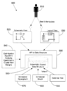
Fig. 5 illustrates a system according to an embodiment of the present
invention.
The system 500 for designs, specifically analog circuit design provides a
direct
representation which the circuit designer can see and manipulate and which the
optimizer
-10-
CA 02415810 2003-01-07
can "see" and manipulate. By contrast, conventional systems which are
typically not
interactive automated systems do not require (and do not use) direct
representations.
Instead, conventional representations are used to allow an optimizer to run.
Such
conventional representations focus on the requirements of the optimizer to
optimize the
design rather than providing a suitable (direct representation) display which
enables the
designer to interactively access, manipulate and guide the optimization
process as it is
conducted by the optimizer. The example of Figs. 8 and 9 illustrate the direct
representation of the circuit 800 by the hyper graph 900. Referring to Fig. 5,
system 500
for analog circuit design includes a storage means such as database 560 for
storing direct
representations of designs. These representations can, for example, be
embodied as
annotated hyper graphs 570, annotated graphs 580 and representations such as
those used
in commercial tools, e.g. Cadence""'s database format 590.
As illustrated in Fig. 5, a designer 510 has access to see and manipulate the
database. A direct representation of the designs is used to provide a one-to-
one
correspondence between each design candidate stored in the database and a
design
represented to the designer in a view. Display interfaces allow the designer
to work with
different views. Each of these interfaces provide views of circuit design
candidates by
using appropriate symbols and conventions. The display interfaces can also
receive
commands by a designer 510 to manipulate the characteristics of the circuit
design
candidates by manipulating the representations of the design candidates. The
designer can
work with more than one view, for example, both a schematic view and a layout
view. Of
course, additional views or alternative views can be used. For example the
schematic
graphical user interface 520 provides a schematic view and a layout graphical
user
interface 530 provides a layout view.
A database interface such as an application programming interface (API) 550 is
used to manipulate the direct representations of circuit design candidates in
the database,
for example, in response to the designer's commands. Accordingly, the system
500 allows
an interactive design approach by designer 510. The designer can interactively
alter data
structures via views which can then immediately be incorporated into the
search. This
speeds up design and increases the designer's control over the design process,
a result that
cannot be achieved by conventional approaches.
-11-
CA 02415810 2003-01-07
The system also includes an optimizer 540 (i.e. the hardware and software
implementation of an optimization algorithm which is part of an automated or
partially
automated iterative design process) which accesses the circuit design
candidates in the
database via the database interface 550. The optimizer 540 is typically a
search engine
which manipulates and acts on the schematics in the database to determine the
most
suitable candidates during the design process. In order to process the
candidate designs in
the database, the optimizer has read access to the database to be able to
determine the
status of the database and current search results. It is in this sense that
the optimizer "sees"
the database. Referring to Fig. 5, this achieved through the API associated
with the
database. The optimizer also requires write access to operate on or manipulate
the current
search to allow evolution of the design candidates towards the final search
results.
Accordingly, a change to a design in the database results in a change in the
visual
display of the design presented to the designer. More importantly, however, a
change
made by the designer during optimization is reflected by a corresponding
change in the
database, which affects the future activity of the optimizer. For example, a
designer
presented with a display such as that of Fig. 8 via an interactive graphical
user interface
can use a pointing device to select and delete a component such as resistor
812. Referring
to Fig. 9, the corresponding node 912 in the direct representation of the
circuit of will also
be deleted and the optimizer will use the resulting modified circuit for
future processing.
Similarly, the designer can add additional components or groups of components
by
graphical user interface tools such as "drag and drop" or selection from a
menu and
replace existing components by other components or groups of components. The
designer
also has the ability to change the relationships between components, for
example, by
changing the points of connection of a resistor. In an alternative view, the
designer can
also change the values associated with any component including such as the
resistance of a
resistor, the physical size of a component or the physical location of the
component.
Typically, the system 500 enables an iterative design process that repeats
until a
suitable stopping condition is realized. During the process, the optimizer
examines design
candidates under consideration and selects or otherwise operates on the
candidates to
improve an evolving subset from which the eventual search results or solution
set will be
selected. According to a preferred embodiment, the designer can use the
interactive
display interface to interactively stop the iterative design (optimization)
process.
-12-
CA 02415810 2003-01-07
The preferred embodiment includes an optimizer that operates on the stored
direct
representations. However, this is not necessary to the practice of the
invention. In other
words, the optimizer can, if desired, perform its optimization process on the
design circuits
after suitably transforming candidate designs into an alternative
representation that need
not be in direct correspondence with the direct representation of the
database. It must,
however, be able to transform in both directions: it must be able to transform
the
alternative representation back into the direct representation, and the direct
representation
into the alternative representation.
Fig. 6 illustrates conceptually the interactive relationship between
manipulation of
designs in the database by the designer and the optimizer. Since the optimizer
also sees
and manipulates the designs in the same database, a change made by the
designer during
runtime ("on-the-fly") updates the infonnation made available to the
optimizer.
Accordingly, the designer 510 can direct or affect the search path or
direction of the
optimizer. Furthermore, changes made by the optimizer will make corresponding
changes
to the displays presented to the designer thereby showing the progress made by
the
optimizer. Changes made by the designer that affect the optimizer will also be
displayed to
the designer who can see the effects of the changes and make further changes
or take other
action such as stopping the search and starting again.
Fig. 10 illustrates a corresponding method in accordance with another aspect
of the
present invention. According to the method, circuit design candidates are
represented
using direct representations 1010. These direct representations are stored in
a storage
medium such as a database or a list of data structures (e.g. a netlist) in
computer memory
(step 1020). Next, new circuit design candidates are generated using the
generator of the
optimizer (step 1030). An "expanded set" of design candidates is created which
includes
the current circuit design candidates along with the new design candidates.
The selector is
used to select one or more preferred design candidates from the expanded set
of design
candidates and these form the updated current design candidates which are then
stored in
the storage medium (step 1040). The method continues to generate, select and
store design
candidates until a stopping criterion is satisfied (step 1050).
An alternative embodiment is illustrated in Fig. 11 which is similar to Fig.
10 but
includes user interactivity by the inclusion of steps 1041 and 1042. In step
1041 views of
one or more of the current design candidates are displayed to the designer
using an
-13-
CA 02415810 2003-01-07
interactive display interface. In step 1042, the designer makes modifications
to these
displayed design candidates via the interactive display interface, which then
stores the
modified designs.
Although the present invention is presented in the context of circuit design
example, method of the present invention is applicable to many other types of
design
problems including, for example, design problems relating to digital circuits,
scheduling,
chemical processing, control systems, neural networks, regression modelling of
unknown
systems, molecular synthesis, optical circuits, photonics, communications
networks,
sensors and flow network design problems such as road systems, waterways and
other
large scale physical networks, optics, mechanical components and opto-
electrical
components.
Embodiments of the present invention can be implemented as a computer-readable
program product, or part of a computer-readable program product, for
distribution or
integration in suitable software and hardware systems. Such implementation may
include a
series of computer instructions fixed either on a tangible medium, such as a
computer
readable medium (e.g., a diskette, CD-ROM, ROM, or fixed disk) or
transmittable to a
computer system, via a modem or other interface device, such as a
communications
adapter connected to a network over a medium. The medium may be either a
tangible
medium (e.g., optical or electrical communications lines) or a medium
implemented with
wireless techniques (e.g., microwave, infrared or other transmission
techniques). The
series of computer instructions embodies all or part of the functionality
previously
described herein. Those skilled in the art will appreciate that such computer
instructions
can be written in a number of programming languages for use with many computer
architectures or operating systems. Furthermore, such instructions may be
stored in any
memory device, such as semiconductor, magnetic, optical or other memory
devices, and
may be transmitted using any communications technology, such as optical,
infrared,
microwave, or other transmission technologies. It is expected that such a
computer-
readable program product may be distributed as a removable medium with
accompanying
printed or electronic documentation (e.g., shrink-wrapped software), preloaded
with a
computer system (e.g., on system ROM or fixed disk), or distributed from a
server over
the network (e.g., the Internet or World Wide Web). Of course, some
embodiments of the
invention may be implemented as a combination of both software (e.g., a
computer-
- 14-
CA 02415810 2003-01-07
readable program product) and hardware. Still other embodiments of the
invention may be
implemented as entirely hardware, or entirely software (e.g., a computer-
readable program
product).
Embodiments of the invention may be implemented in any conventional computer
programming language. For example, preferred embodiments may be implemented in
a
procedural programming language (e.g. "C") or an object oriented language
(e.g. "C++").
Alternative embodiments of the invention may be implemented as pre-programmed
hardware elements, other related components, or as a combination of hardware
and
software components.
The above-described embodiments of the present invention are intended to be
examples only. Alterations, modifications and variations may be effected to
the particular
embodiments by those of skill in the art without departing from the scope of
the invention,
which is defined solely by the claims appended hereto.
-15-