Note: Descriptions are shown in the official language in which they were submitted.
CA 02415979 2003-O1-06
INTERCONNECTION SYSTEM
Claim of Priority and Cross-reference to Related Applications
[001] The present application is a Continuation-In-Part of parent U.S. Patent
,Application
Serial No. 10/036,796, filed in the U.S. Patent and Trademark Office on
January T, 2002 and
priority is hereby claimed under 35 USC 120 of the parent application and of
Provisional Patent
Application Serial No. 60/260,893 filed in the U.S. Patent and Trademark
Office on January 12,
2001, entitled "HIGH SPEED, HIGH DENSITY INTERCONNECT SYS7,EM FOR
DIFFERENTIAL AND SINGLE-ENDED TRANSMISSION APPLICATIONS" and Provisional
Patent Application Serial No. 60/328,396 filed in the U.S. Patent and
Trademark. Office on
October 12, 2001, entitled "HIGH SPEED, HIGH DENSTTY INTERCONNECT SY;>TEM FOR
DIFFERENTIAL AND SINGLE-ENDED TRANSMISSION APPLICATIONS", upon which
the parent application is based. The disclosures of these applications are
hereby incorporated by
reference in their entirety into the present specification.
Background of the Invention
Field of the Invention
[002] The present invention relates generally to electrical interconnection
systems, and more
particularly, to a high speed, high-density interconnection system for
differential and single-
ended transmission applications.
CA 02415979 2003-O1-06
Description of the Related Art
[003] Backplane systems are comprised of a complex printed circuit board that
is referred to
as the backplane or motherboard, and several smaller printed circuit boards
which are referred to
as daughtercards which plug into the backplane. Each of the daughtercards may
include a chip
that is referred to as a driver/receiver. The driver/receiver sends and
receives signals from
driver/receivers on other daughtercards. A signal path is formed between the
driverlreceiver on a
first daughtercard and a driver/receiver on a second daughtercard. The signal
path includes an
electrical connector that connects the first daughtercard to the backplane,
the backplane, a second
electrical connector that connects the second daughtercard to the backplane,
and the second
daughtercard having the driver/receiver that receives the carried signal.
Various driver/receivers
being used today can transmit signals at data rates between 5-10 Gb/sec and
greater. The
limiting factor (data transfer rate) in the signal path is the electrical
connectors which connect
each daughtercard to the backplane. A need thus exists in the art for a high-
speed electrical
connector capable of handling the required high-speed transfer of data.
[004] Further, the receivers are capable of receiving signals having only 5%
of the original
signal strength sent by the driver. This reduction in signal strength
increases the importance of
minimizing cross-talk between signal paths to avoid signal degradation or
errors being
introduced into digital data streams. With high speed, high-density electrical
connectors, it is
even more important to eliminate or reduce cross-talk. Thus, a need exists in
the art for a high-
speed electrical connector capable of handling high-speed signals that reduces
cross-talk between
signal paths.
[005] There are various types of electrical connectors. ~ne type is a through
hole: connector
which could either be a compliant pin or through hole solder. Backplane
systems have typically
used connectors that consist of multiple contacts having pins that are
inserted into the through
hole contained in the printed circuit boards to be connected. The pins can be
compliant fit or can
be soldered in place. These require a relatively large diameter hole in the
printed circuit board
for receiving the pins of the connector. The larger the hole, the greater the
probability of defects
2
CA 02415979 2003-O1-06
from plating and the greater the capacitance that reduces the signal speed
which Call be
accommodated by these connectors. For example, plated through holes may not
be: properly
plated and thus pins being inserted from the electrical connector can cause
opens, shorts, etc. A
plated through hole causes a capacitive effect which reduces the data rate
which can be
transferred through the pin and hole. Further, many contact type connectors
are made from
stamped parts that have varying geometries that increase signal reflection and
reduce signal
speed. Thus, it is advantageous to reduce the diameter of plated through holes
using
compression mount-type connectors that rely on a spring making contact with a
pad on a board.
[006] Many of these problems can be solved using a compression mount type
electrical
connector. This type of connector overcomes many of the deficiencies of the
through hole
contact type but compression mount connectors need bulky and expensive
hardware to fasten the
compression mount connector to the printed circuit board. Intimate contact
needs to be
maintained between compression mount contacts and the PC board surface without
using
additional fasteners such as jack screws.
[007] Additionally, regardless of the type of electrical connector, the
electrical connector has
to be capable of being mated/unrnated at least 250 and perhaps in excess of
1000 times. If the
contacts wear, then contact resistance will increase. Contact wear can occur
through metal-to-
metal contact either through a point or line. For example, a certain area may
continually get
wiped as the connector is mated/unmated and the contact tends to wear through
the mfaal sliding
action can also cause wear. Also, some compression mount type connectors use
dendrite
contacts on flexible circuits. One difficulty with dendrite contacts is that
these contacts tend to
wear and are only good for a half a dozen mating cycles and the dendrites
start to flatten out and
the multiple points of contacts are lost thereby reducing reliability. Thus, a
need exists for a
compression mount-type connector that eliminates or reduces contact wear.
[008] Another problem with prior art electrical connectors is that impedance
changes over
the length of the signal path reduce the potential signal speed. A need exists
for an electrical
3
CA 02415979 2003-O1-06
connector in which impedance can be controlled at a specific value and where
the specific value
remains relatively constant over the length of the signal path.
[009] In summary, electrical connectors used to electrically connect circuit
boards such as
backpanels to daughtercards suffer from several deficiencies including poor
shielding resulting
in electrical noise, changes in impedance and the inability to connect and
disconnect many times
without damage to the electrical connector. These deficiencies limit the data
rate that can be
transferred through the connector. Thus, a need exists in the art for a high-
density electrical
connector that overcomes the aforementioned problems to a large extent.
Summary of the Invention
[0010] It is an object of the present invention to provide an electrical
interconnection system
capable of carrying signals at data rates between ~-10 Gb/sec or more.
[0011] Still another object of the present invention is to provide an
electrical connector
having a differential pair having constant impedance over the signal path and
capable of carrying
signals at between 5-10 Gb/sec or more.
[0012] Yet another of the present invention is to provide a coaxial cable
connector having
constant impedance over the signal path and capable of carrying signals at
data rates between 5-
Gb/sec or more.
[0013) Another object of the present invention is to provide an electrical
connector in which
cross-talk between signal paths of adjacent twinax cables or adjacent coaxial
cables within the
electrical connector is reduced and/or eliminated.
[0014] Yet another object of the present invention is to provide a compression
type electrical
connector using a conductive spring configuration.
CA 02415979 2003-O1-06
[0015] The present invention is directed to a high-density electrical
connector that can
provide 40 or more twinax connections per linear inch in a 25 millimeter or
less card slot. In a
typical electronic system package, 20 millimeters is the spacing from center-
line to center-line of
the adjacent parallel daughtereards. Twinax cable is coaxial cable that
contains two inner
conducting wires rather than one. The two inner conducting wires provide two
physical
channels. Coaxial cable is called "coaxial" because it includes one physical
channel i:hat carries
the signal surrounded (after a layer of insulation) by another concentric
physical channel, both
running along the same axis. The outer channel serves as ground.
[4016] These and other objects of the present invention may be achieved by
providing an
interconnection system comprising: a plurality of spacers arranged to be
disposed adjacent each
other in a row having two ends, each spacer including at least one groove
arranged to allow a
cable section to be disposed therein upon said spacer being disposed adjacent
to another of said
plurality of spacers; a plurality of cable sections respectively disposed
within said grooves of
said plurality of spacers, each cable section having first and second ends and
at least one center
conductor and an outer conductive shield, and said grooves of said plurality
of spacers being
arranged so as to leave exposed, on a first plane, all of said first ends of
said plurality of cable
sections and so as to leave exposed, on a second plane, all of said second
ends of said plurality of
cable sections; a pair of end pieces respectively arranged to be disposed
adjacent said to ends of
said row of plurality of spacers; first and second interposers respectively
arranged to be disposed
adjacent said first and second planes, each interposer having an aperture for
each center
conductor of said plurality of cable sections and having at least one aperture
for each outer
conductive shield of said plurality of cable sections; and a plurality of
electrically conductive
contacts, each electrically conductive contact having first and second ends
and being arranged to
be respectively disposed in one of said apertures of said first and second
interposers, wherein
said first end of each of said plurality of electrically conductive contacts
respectively makes
electrical contact with one of said plurality of cable sections and wherein
said second end of each
of said plurality of electrically conductive contacts extends through its
respective aperture in its
respective interposer beyond a plane of said interposer.
CA 02415979 2003-O1-06
[0017] These and other objects of the present invention may alsa be achieved
by
providing a method of manufacturing an interconnection system, the method
comprising:
disposing a plurality of spacers adjacent each other in a row having two ends;
arranging each
spacer to include at least one groove to allow a cable section to be disposed
therein upon said
spacer being disposed adjacent to another of said plurality of spacers;
respectively disposing a
plurality of cable sections within said grooves of said plurality of spacers,
each cable section
having first and second ends and at least one center conductor and an outer
conductive shield;
arranging said grooves of said plurality of spacers so as to leave exposed, on
a first plane, all of
said first ends of said plurality of cable sections and so as to leave
exposed, on a second plane,
all of said second ends of said plurality of cable sections; respectively
disposing a pair of end
pieces adjacent said to ends of said row of plurality of spacers; respectively
disposing first and
second interposers adjacent said first and second planes, each interposer
having an aperture far
each center conductor of said plurality of cable sections and having at least
one aperture for each
outer conductive shield of said plurality of cable sections; and respectively
disposing a plurality
of electrically conductive contacts, each electrically conductive contact
having first and second
ends, in one of said apertures of said first and second interposers; wherein
said first end of each
of said plurality of electrically conductive contacts respectively makes
electrical contact with one
of said plurality of cable sections; and wherein said second end of each of
said plurality of
electrically conductive contacts extends through its respective aperture in
its respective
interposer beyond a plane of said interposer.
[0018] Still furthermore, these and other objects of the present invention may
be achieved by
providing an interconnection system comprising: a plurality of spacers
arranged adjacent each
other in a row; a plurality of cable sections, each of said plurality of cable
sections having at least
one center conductor and an outer conductive shield and each of said cable
sections being
disposed within at least one of said plurality of spacers, and all of said
plurality of cable sections
having one end exposed on a first plane and a second end exposed on a second
plane; a pair of
interposers having apertures disposed therein, said pair of interposers being
respectively disposed
on faces of said plurality of spacers; and electrically conductive contacts
respectively disposed
within said apertures in said pair of interposers so as to have one end making
electrical contact
6
CA 02415979 2003-O1-06
with one of said cable sections and another end extending through its
respective aperture in its
respective interposer.
[0019] Lastly, these and other objects of the present invention may be
achieved by
providing a method of manufacturing an interconnection system, the method
comprising:
arranging a plurality of spacers adjacent each other in a row; disposing each
one of a plurality of
cable sections within at least one of said plurality of spacers, each of said
plurality of cable
sections having at least one center conductor and an outer conductive shield
and all of said
plurality of cable sections having one end exposed on a first plane and a
second end exposed on a
second plane; respectively disposing a pair of interposers on faces of said
plurality of spacers,
each of said pair of interposers having apertures disposed therein; and
respectively disposing
electrically conductive contacts within said apertures in said pair of
interposers so as to have one
end making electrical contact with one of said cable sections and another end
extending through
its respective aperture in its respective interposer.
[0020] In the present invention, each of said electrically conductive contacts
may
comprise a spring contact disposed within a top hat, an exposed end of said
spring contact
comprising said first end of said respective electrically conductive contact
and a closed end of
said top hat comprising said second end of said electrically conductive
contact and each top hat
may include a shoulder portion in a plane perpendicular to an axis thereof.
[0021] Furthermore, in the present invention, each of said electrically
conductive contacts
may comprise a one-piece semi-rigid spring contact having :first and second
ends, said first end
of said spring contact comprising said first end of said respective
electrically conductive contact
and said second end of said spring contact comprising said second end of said
electrically
conductive contact. each spring contact includes a shoulder portion in a plane
perpenf~icular to an
axis thereof and each cable section may comprise two center conductors.
[0022] Lastly, in the present invention, each interposer may have two
apertures for each outer
conductive shield of said plurality of cable sections and an exposed
respective end of said at least
7
CA 02415979 2003-O1-06
one center conductor and an outer conductive shield of said first end and said
second end of each
cable section may be in one plane.
[0023] Still other advantages of the present invention will become readily
apparent to those
skilled in the art from the following detailed description, wherein
embodiments of the invention
are shown and described, simply by way of illustration. As will be realized,
the invention is
capable of other and different embodiments, and its several details are
capable of modifications
in various respects, all without departing from spirit and scope of the
present invention.
Accordingly, the drawings and description thereof are to be regarded as
illustrative in nature, and
not as restrictive.
Brief Description of the Drawings
[0024] The present invention i.s illustrated by way of example, and not by
limitation, in the
figures of the accompanying drawings, wherein elements having the same
reference numeral
designations represent like elements throughout and wherein:
[0025] Figure 1A is a perspective view of an electrical connector according to
an embodiment
in accordance with the invention disclosed in the parent application mounted
to a daughtercard
and a backplane with an over-mold omitted for clarity.
[0026] Figure 1B is the same view as Figure 1 A with the over-mold depicted.
[0027] Figure 2 is a perspective view of the electrical connector according to
an embodiment
in accordance with the invention disclosed in the parent application with the
semi-rigid twinax
connected to the back panel interposer only and with the. backpanel and over-
mold omitted for
clarity.
[0028] Figure 3 is a bottom perspective view of Figure 2,
[0029] Figure 4 is the same view as Figure 2 with the back panel interposer
omitted far
clarity.
8
CA 02415979 2003-O1-06
[0030] Figure 5 is the same view as Figure 4 with some of the spring contacts
omitted for
clarity.
[0031] Figure 6 is the same view as Figure 5 with additional spring contacts
omitted for
clarity.
[0032] Figure 7 is a bottom perspective view with the spring contacts omitted
for clarity.
[0033] Figure 8 is a perspective view of the daughtercard and backpanel
including; PC board
patterns.
{0034] Figure 9 illustrates a baekpanel, mid-panel and daughtercard in an
actual application.
[0035] Figure 10 is an exploded view of a second embodiment of an electrical
connector
according to the principles of the invention disclosed in the parent
application.
[0036] Figure 11 is an enlarged exploded view of the cable housing
interposers.
[0037] Figure 12 is an enlarged view of a front side of the interposer cable
housing shown in
Figure 10.
[0038] Figure 13A is a perspective view of the electrical connector of the
parent application
mounted to a daughtercard with the daughtercard interposer slide being in a
retracted position
and the backpanel interposer slide being in an extended position.
[0039] Figure 13B is a cross-sectional view of spring contacts being retained
by the Mylar
sheet illustrating one end of the spring contacts within the interposer slide
when the interposer
slide is in an extended position.
[0040] Figure 13C is a cross-,sectional view similar to Figure 13B
illustrating the one end of
the spring contacts extending beyond the interposer slide when the interposer
slide is in a
retracted position.
s
CA 02415979 2003-O1-06
[0041] Figure 14 is an exploded view of an example embodiment of an electrical
connector
according to the principles of the present invention.
[0042] Figure 15 is a view of a partially assembled connector according to the
principles of
the present invention.
[0043] Figure 16 is a view of portions of the connector according to the
principles of the
present invention.
[0044] Figure 17 is a view of the connector according to the principles of
th.e present
invention prior to the attachment of the interposers.
[0045] Figure 18 is a view of one interposer of the connector of Figure 14.
[0046] Figure 19 is a view of the interposer of Figure 18 with one set of top
hats
inserted therein.
(0047] Figure 20 is a view of the interposer of Figure 19 with one set of
spring
contacts. respectively against in the one set of top hats.
[0048] Figure 2I is a view of the interposer of Figure 20 with one end of a
single
twinax cable arranged with one set of spring contacts and top hats.
[0049] Figure 21 A is a close-up view of a portion of the arrangement of
Figure 21
with some elements being omitted for clarity.
[0050] Figure 22 is a view corresponding to that of Figure 21 but with all of
the
twinax cables being arranged with their respective spring contacts and top
hats.
[0051] Figure 23 is a view of the connector of Figure 22 after encapsulation.
[0052] Figure 24 is a view of the connector of Figure 23 after attachment of
the
interposers.
CA 02415979 2003-O1-06
Detailed Description of the Invention
[0053] The interconnect arrangement according to the present invention
provides a unique
twin axial shielded coax structure that has constant impedance from
daughtercard interface to the
backplane interface. The coaxial structure provides for constant impedance of
65 ohms single
ended impedance, 50 ohms odd mode impedance and 100 ohms differential
impedance.
Advantageously, the present invention provides a controlled impedance
connector through the
ability to change the characteristic impedance of the electrical connector by
changing the
dielectric thickness and constant. This allows custom connectors to be made at
different
impedance values ranging from 30 ohms to 150 ohms or higher.
[0054] A single ended interconnect path utilizes one conductor to transfer
data. A differential
interconnect path utilizes two conductors to transmit the same data. The
benefit of a differential
interconnect path relative to a single ended interconnect path is that
transmission speed increases
and noise immunity and electro-magnetic interference (EMI) concerns are
reduced.
[0055] Utilizing the twinax design according to the present invention, the
connector design
described herein will provide the best known practice for transmitting
differential data utilizing
copper conductors. The same i s true for the single ended version. The single
ended design
utilizes a coaxial conductor to transmit data. This makes it possible to
transmit analog (RF) or
digital data with signal degradation comparable to that of a coaxial cable.
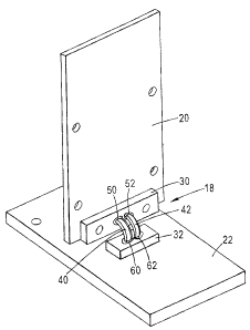
[0056] Refer first to Figures 1A and 1B where an interconnect system for a
high speed, high
density interconnect path is illustrated. Figure 1 A shows the electrical
connector with the over-
mold omitted for simplicity of explanation. The connector 18 is used to
electrically connect
daughtercard 20 to a backpanel 22. The connector 18 includes, as depicted in
Figure 1B, a
daughtercard interposer 30, a backpanel interposer 32, an over-mold 34 which
over-molds semi-
rigid twinax or coax cables. The over-mold 34 is preferably injection molded,
for example, from
PBT (polybutylene terephthalate). As depicted in Figures 1A and IB, only two
twinax cables 40,
42 are shown for ease of illustration, although it is anticipated that 80
pairs or more of twinax
may be used in the electrical connector. This embodiment uses twinax cable
that is bent into a
11
CA 02415979 2003-O1-06
desired shape. A more rigid construction that is molded in a single piece may
also be used. For
the cables 40 and 42, the center conductor is copper, the dielectric material
may be TeflonTM and
the outside jacket may be a braid. Preferably, the differential impedance
between center
conductors is approximately 100 ohms. Using standard formulas, the impedance
cam easily be
adjusted by varying the distance between center conductors and the dielectric
constant for
example. In Figure 1A, the over-mold 34 is omitted for clarity. As depicted in
Figures 1A and
1B, spring contact arrangements S0, 52, 60, 62 are positioned within the
interposers 30 and 32,
respectively, and surround ends of the twinax cables 40 and 42 in order to
shield the twinax
cables and control the impedance of the connector.
[0057] Spring contacts and the uses thereof are explained in U.S. Patent No.
4,998,:306, issued
January 29, 1991, entitled "LOW-LOSS ELECTRICAL INTERCONNECTS", U.S. Patent
No.
5,886,590, issued March 23, 1999, entitled "MICROSTRIP TO COAX VERTICAL
LAUNCHER USING FUZZ BUTTON AND SOLDERLESS INTERCONNECTS", 11.S. Patent
No. 6,039,580, issued March 21, 2000, entitled "RF CONNECTOR HAVING A
COMPLIANT
CONTACT", U.S. Patent No. 4,924,918, issued May 15, 1990, entitled "MALI= INE
FOR
MANUFCTURING BUTTON CONNECTOR AND METHOD THEREFOR", and 1J.S. Patent
No. 5,007,843, issued April 16, 1991, entitled "HIGH-DENSTTY CONTAC'.T AREA
ELECTRICAL CONNECTORS", all of which are hereby incorporated by reference in
their
entirety into the present specification. Although the present invention
described herein is
described with respect to the illustrated type of spring contacts, it should
be understood that they
are an illustrative type of conductive element or contact and that other types
of electrically
conductive elements or springs can be used with the present invention. The
conductive element
provides high reliability, multiple points of contact and is randomly
compressed into a. shape that
provides multiple electrical contact points to a mating surface.
[0058] The conductive element may take various suitable forms. For example,
the conductive
element may include a "watch lband" or POGO" pin, that is, at least one spring-
loaded pin
capable of being compressed. In a further alternative, the conductive element
may include a
bellows device comprising a plurality of deformable folds that are
compressible. A further
12
CA 02415979 2003-O1-06
suitable conductive element comprises a conductor formed into a plug-shaped
compressible
mesh. Alternatively, the conductive element may include Belleville washers or
an element
comprised of an elastomer loaded with conductive particles. Preferably, the
conductive element
is plated with gold in order to ensure low, stable RF losses in benign or
adverse environments.
[0059] The conductive element may comprise a single element as described
above, or other
types suitable for providing at least one compliant end or, alternatively, may
comprise more than
one element, in which case at least one of the elements has at least one
compliant end.
[0060] Although a right angle connector 18 is illustrated, it should be
understood that other
configurations, such as straight configurations between parallel circuit
boards, are possible.
Also, although the following discussion is with respect to daughtercards and
backpanels, this is
only done for convenience and it should be understood that the electrical
connector discussed
below is usable for connecting all types of circuit boards as well as in other
high speed
applications.
[0061] As illustrated in Figures 1A and 1B, the connector 18 would be
assembled by
connecting interposer 30 and the backpanel interposer 32. As depicted in
Figure 1B, the
connector 18 is assembled as follows. First, the twinax cables 40, 42 are
formed. All of the
spring contacts are installed into interposers 30 and 32. The twinax cables 40
and 42 are then
installed into the interposers 30 and 32. -The assembly is then insert molded
to form the over-
mold 34 that makes the entire electrical connector 18 rigid. The over-mold 34
is preferably PBT.
The electrical connector 18 could then be connected to the daughtercard 20
using fasteners such
as screws, rivets, compression posts, and the like.
[0062) The spring connectors 50, 52, 60, and 62 can be made from a single gold
plated fine
wire that is compressed into a very small shape. The 'resulting object is a
wire mass having
spring performance and demonstrates superior electrical signal conduction from
high current DC
to microwave frequencies. The typical size of such a spring contact is 0.01
inch in diameter by
0.060 in length. The signal carrying spring contacts preferably have the same
outer diameter as
the signal carrying center cable. The ground contact spring contacts do not
have to t>e the same
13
CA 02415979 2003-O1-06
diameter or length as the signal carrying spring contacts. The spring contacts
50, 52, 60, and 62
are employed in the illustrative embodiments, preferably each formed from a
strand of metal
wire, each strand being wadded together to form a desired cylindrically shaped
''button" of
material having a density of between 20% and 30%. As depicted in Figures 1A
and 1B, each
wadded-wire connected spring contact fits snuggly in openings of the
daughtercard interposer 30
and the backpanel interposes 32. Each wadded-wire spring contact 50, 52, 60,
and 62 makes
electrical contact at multiple points when compressed against the contact
area. Connectors of
this type have significant advantages over other types of connectors and
provide connections of
high integrity and reliability. In contrast to other types of connections,
this mechanical connector
element has very few associated variables that can affect the quality of the
connection.. The only
significant variables are the size of the connector element and the
compressive force used to
make the connection, both of which can be accurately controlled by controlling
the volume into
which the spring contact is placed. Alternatively, in high vibration
environments, the spring
contact can be affixed in place using a conductive epoxy.
[0063] The spring contacts employed in the illustrative embodiments can be
fabricated using
nickel wire, or wire made from alloys such as beryllium and copper, silver and
copper, or
phosphorous and bronze. The compression of the wadded wire of the spring
contacts is
substantially elastic so that, when the compressive force of the twinax cables
is removed, the
spring contacts return to their original shape. The wire is randomly
compressed into a. cylindrical
shape and the wire has some spring constant associated with it to provide
resiliency when
pressure is applied. Advantageously, this allows the electrical connector 18
to be connected and
disconnected as many times as is needed. In the embodiments described above,
the wadded-wire
connector elements 50, 52, 60, and 62 can comprise components manufactured by
Technical
Wire Products, Inc. of Piscataway, New Jersey, under the trademark Fuzz
ButtonTM.
[0064] Referring now to Figure 2, the twinax cables 40 and 42 are inserted
into thc~ backpanel
interposes 32. Figure 2 differs from Figure 1 in that two twinax cables 40 and
42 are depicted
instead of one. It is important to note that central conductors 120 and 122
are not shielded from
14
CA 02415979 2003-O1-06
each other. However, it is important to shield twinax pairs from each other as
depicted in Figure
2.
[0065] As depicted in Figure 2, the backpanel interposes 32 has two opposed U-
shaped
openings 100 and 102 each respectively having an outer U-shaped peripheral
wall 110 and 112,
an inner U-shaped peripheral wall 117 and 118 and a straight wall 114 and 116,
respectively.
Walls 114 and 116 face each other as depicted in Figure 2. Inserted into the U-
shaped openings
are a plurality spring contacts 200, 202, 204, and 206, respectively, each
being in a half U-shape
as depicted in Figure 2. For example, spring contacts 200 and 202 each have a
half U-shape and
when placed together form a U partially surrounding the twinax cable 40. It
should be
understood that other shielding methods could be used to replace the spring
contacts.
[0066) The twinax cable 40 has two central conductors 120 and 122 surrounded
b;y TeflonTM
sheathing 124, for exarnpIe. Preferably, signal carrying spring contacts 300-
306 (see Figure 3)
have the same outer diameters as the two central conductors 120, 122. The
TeflonT~t sheathing
124 may be covered by an electrically conductive copper layer or by a rigid or
semi-rigid outer
case 128 made of copper and aluminum or a tin filled braiding. Case 128 may be
formed using a
plating process. As depicted in Figure 2, the rigid outer case 128 is stripped
away to a length E,
thereby exposing the TeflonT'~~ sheathing 124. The TeflonTM sheathing 124 is
stripped away
from the central conductor to a length F. This stripping is done symmetrically
on both ends of
twinax cables 40 and 42. The spring contacts 200, 202, 204, and 206 are in
electrical contact
with the layer 128 so as to form a shield.
[0067] Refer now to Figure 3 that depicts a bottom view of Figure 2. Mounted
within the
interposes 32 are spring contacts stacked one upon another in a half U-
configuration ithrough the
thickness of interposes 32 for surrounding and shielding the central twinax
leads 120 and 122,
respectively, of twinax cables 40 and 42. Also depicted are a plurality of
vertically extending
cylindrical spring contacts 210, 212, and 214 that are positioned between
walls 114 and 116.
The spring contacts 210 and 214. extend through the thickness of interposes 32
and are used to
shield twinax cables 40 and 42 from each other. As depicted in Figure 3, it
should be understood
CA 02415979 2003-O1-06
that there is a full 360° shielding for twinax cables 40 and 42 for the
stripped away portions of
coax cables 40 and 42 that extend through the interposer 32. As depicted in
Figure 3, there are
four spring contacts 300, 302, 304, and 306 in contact with the exposed
portions of central
conductors 120 and 122 of twinax cables 40 and 42.
[0068] Figure 4 is an illustration similar to Figures 2 and 3 in which the
daughtercard
interposer 32 has been omitted for clarity. As is evident in Figure 4, there
are four stacks of half
U-shaped spring contacts 200, 222, 224, 226, 228; 202, 232, 234, 236, 238; and
204, 242, 244,
246, 248, 206, 252, 254, 256, and 258 (not shown). These four stacks together
with the
vertically extending spring contacts form a full 360° shield around
twinax cables 40 and 42. It is
envisioned that the uppermost and lowermost' spring contacts will be used.
However, it is
possible to use structures other than spring contacts to electrically connect
the uppermost and the
lowermost spring contacts. For example, a stamped and formed metal component
(not shown)
can be used to electrically connect the uppermost and the lowermost spring
contacts.
[0069] Figure 5 is similar to Figure 4 except that spring contacts 200, 222,
224, 226 and 228
have been omitted to show spring contacts 306, and 304 respectively in contact
wiah central
conductors 122 and 120.
[0070] As depicted in Figure 6, it can be seen that spring contacts 300 and
302 and also 304
and 306 (not shown) contact the exposed portions of the central signal
carriers 120' and 122.
These spring contacts 300-306 are the signal carrying spring contacts. It is
important that the
signal carrying spring contacts are substantially the same diameter as the
twinax central
conductors 120 and 122 to maintain constant impedance. It is also envisioned
that other types of
spring contacts could be used in the present invention. For example,
conductive textiles may be
used. Compression springs could also be used. The conductive textile may be
injected into the
connector replacing the spring contacts.
[0071] Refer now to Figure 7 where a bottom perspective view of the electrical
connector 18
is depicted. As depicted in Figure 7, a central portion 701 is formed between
the straight wall
114 and the bottom of the outer lJ-shaped wall 110. The central portion 701
includes through
16
CA 02415979 2003-O1-06
holes 700 and 702 that receive vertically extending spring contacts 300 and
302. A wall 704 is
formed centrally in the U-shaped area to form a first half U-shaped opening
710 and a second U-
shaped opening 712 which respectively receive spring contacts 206, 252, 254,
256, and 258 and
204, 242, 244, 246, and 248. It is envisioned that there could be a two- piece
construction and
the center support structure could be a separate member constructed of a
TeflonT~r dielectric.
Also, metal plated plastic components could be used.
(0072] As depicted in Figure 8, a plurality of electrically non-conductive
patterns 402
and 404 are on the daughtercard 20 and the backpanel 22, respectively. The
pattern 402 has an
electrically conductive area 410 having roughly a figure eight configuration.
The patterns can be
formed using known photolithographic techniques. A first non-conductive area
412 and a
second non-conductive area 414 are spaced apart from each and within an outer
periphery 420 of
the pattern 402. The first non-conductive area 412 has two areas 430 and 432
that include
conductive pads 440 and 442. The second non-conductive area 414 has two areas
4:34 and 436
that include conductive pads 444 and 446. Openings 430, 432, 434, and 436
receive the center
conductors 120 and 122 of twinax cables 40 and 42 that extend from the
interposes 30 such that
spring contacts 300, 302, 304, and 306 are respectively brought into contact
with the conductive
pads 440, 442, 444, and 446. Referring back to Figure 4, spring contacts 228,
238, 248 and 258
will be in electrical contact with the electrically conductive area 410. In
this manner., the spring
contacts provide a shielding path to ground. The electrically conductive area
410 is connected to
ground plane on the daughtercard and on the backplane. The inner surfaces of
openings 430,
432, 434, and 436 are electrically conductive and are connected to signal
paths so that spring
contacts 306, 304, 302, and 300 are in electrical contact therewith when the
interposes 30 is used
to connect the daughtercard 20 and the backpanel 22. Spring contacts are
mounted in the
interposes 32. Advantageously, 'the spring contacts 300, 302, 304, and 306
will be compressed
when the daughtercard and backpanel are mated which provides a normal force on
the; signal line
and on the cable. The spring contacts 300, 302, 304, and 306 and 228, 238,
248, and 258 will be
compressed to the board 20 maintaining normal forces with respect to the
daughterc;ard pattern
402. The pattern 404 on the backpanel 22 is the same as the pattern 402 and
need not be
described in detail herein. The pattern 404 includes an electrically
conductive portion 458 and a
17
CA 02415979 2003-O1-06
first non-conductive area 460 and a second non-conductive area 462.
Advantageously, the
electrical connector 18 can be connected and reconnected multiple times
without degrading the
signal contacts 300, 302.
[0073] Refer now to Figure 9 where a backpanel 700 is depicted connected to 'a
daughtercard 710. Such an arrangement is also usable in mid-plane connectors
su<;h as mid-
plane connector 600 depicted in Figure 9 that is connected to a daughtercard
610.
[0074] Refer now to Figure 10 illustrating an electrical connector 1000. At
the outset
it should be noted that the electrical conductors 1020, 1022, and 1024 have
the same electrical
characteristics as electrical conductors as 40 and 42 discussed above. As
depicted in Figure 10,
an electrical conductor 1024 has the shortest path and an electrical conductor
1020 has the
longest path. Referring to Figure 1 l, for example, conductor 1020 has a
downwardly extending
straight portion 1020', an angled portion 1020" and a horizontally extending
strail;ht portion
1020"'. The straight portions 1020' and 1020" facilitate installation of ends
of the conductor
1020 into cable housing interposers 1030 and 1032, as explained below. For
ease of explanation,
only the housing for conductors 1020, 1022, and 1024 is explained here,
although other sets of
conductors are illustrated which have the same housings. Figures 11-13C
illustrate additional
details of the aforementioned arrangement.
[0075] Referring again to Figure 10, the electrical connector 1000 includes
opposed
guide blocks 1002 and 1004 mounted on opposite ends of the electrical
connectc>r 1000, as
discussed in detail below. The guide blocks 1002 and 1004 and the cable
housings 1006-1014
can either be formed of individual molded parts as depicted and assembled
together or can be
formed as an over-molded assembly as described previously with respect to
Figure 1B. In
between guide blocks 1002 and 1004 are a plurality of sets of electrical
conductors. As used
herein, conductors 1020, 1022, and 1024 form one vertical set of conductors.
As illustrated in
Figure 10, there are four horizontal sets of three vertically stacked
electrical conductors forming
a vertical and horizontal array of twinax cable conductors, although it should
be appreciated that
any number of electrical conductors could be used. For example, instead of
four sets of
18
CA 02415979 2003-O1-06
conductors, there could be eight sets of conductors. Alternatively, there
could be, instead of a
stack of three conductors, there could be stacks of two conductors or four or
five conductors
depending on the application.
[0076] Each of the electrical conductors 1020, 1022, and 1024 are retained by
cable housings
1006 and 1008 and the other electrical conductors are retained by the
respective cable housings
1008-1014. 'As depicted in Figure 10, cable housing 1006 is specially adapted
to mate with the
guide block 1002 using horizontal pins 1006', 1006" and 1006"' which interlock
with
corresponding holes 1002', 1002" and 1002"' in the guide block 1002. Housings
1006 and 1008
each include recesses 1007, 1009, and 1011 and 1013, 1015, and 1017,
respectively. Each cable
housing includes a boss and a hole, for example, in cable housing 1008, there
is a boss 1023 and
a hole 1025 for interlocking with the cable housing 1006.
[0077] As depicted in Figure 10, the electrical connector 1000 is a right
angle (that is,
90 degree) electrical connector, although other configurations such as a
straight connector can be
arranged.
[0078] The electrical connector 1000 includes a central twinax or coax portion
1001
that includes all of the copper wire conductors 1020, 1022, and 1024 and all
of the :interlocked
cable housings 1006-1012, and the guide blocks 1002 and 1004. As depicted in
Figure 10, there
is a front rectangular surface 1026 and a bottom rectangular surface 1028 to
the assembled
central assembly 1001. Opposite ends of the conductors 1020, 1022, and 1024
extend slightly
beyond the surfaces 1026 and 1028, respectively, exposing the outer jacket 128
of each of the
twinax conductors 1020 and 1024. The central conductors 120 and 122 extend
slightly beyond
the dielectric 124 and the outer jacket 128 of the twinax conductors 1020 and
1024.
[0079] A rectangular interposer 1030 has a front surface 1030' and a back
surface
1030". The interposer 1030 (that is, surface 1030') mates with the front
surface 1026 of the
assembly 1001. A second rectangular interposer 1032, having a front surface
1032' and a back
surface 1032", mates (that is, surface 1032') with the bottom surface 1028 of
the assembly 1001.
19
CA 02415979 2003-O1-06
The copper wire conductors 120 and I22 engage with the interposers 1030 and
1032 as
explained below.
[0080] Spring contacts 1034 and 1036 are respectively retained by Mylar
retainers 1038 and
1040. The Mylar retainers 1038 and 1040 could be made from any suitable
material including
heat shrinkable plastic. The spring contacts 1034 and 1036 are strategically
placed and extend
within interposes cable housing 1030 and 1032 and interposes slides 1042 and
1044,
respectively. The front surface 1030' of the interposes 1030 is rigidly
mounted to the front
surface 1026 by either press fit studs, ultrasonic welding or epoxy. A pair of
opposed pins 1009
and 1009' extend from the surface 1026 and the guide blocks 1002 and 1004,
respectively, into
recessed holes that (not shown) extend inwardly from the surface 1030'. The
pins 1009 and
1009' keep the interposes 1030 aligned with the cable housings 1006-1014. Pins
(not shown)
extend from the surface 1026 of the guide blocks 1002, 1004 to keep the
interposes 1032 aligned
with the cable housings 1006-1014. The spring contacts 1034 and 1036 include
ground contact
spring contacts and signal carrying spring contacts as explained below. A pair
of guide pins
1046 and 1048, are provided on the backpanel for mounting the electrical
connector 1000
thereto. Guide pins 1046 and 1048 extend through holes 1050 and 1035 and 1048
and 1033,
respectively, and mate with the latching mechanisms. As depicted in Figure 10,
a cylindrical
guide socket body 1003 extends from the guide block 1002 for receiving the
guide pin 1048.
Guide block 1004 has a similar guide socket body (not shown) for receiving
guide pin 1046. The
guide blocks 1002 and 1004 each have a threaded insert 1027 and 1029,
respectively, positioned
at right angles from the guide socket body 1003 and aligned with corresponding
holes 1061 and
1063 in interposes 1030 and holes 1080 and 1082 in the interposes slide 1042.
Threaded
fasteners extend from the daughtercard to fasten the electrical connector 1000
to be threaded into
the threaded inserts 1027 and 1029.
(0481] Turning now to Figure 11, it can be more clearly seen that the lVylar
sheet
1038 includes a plurality of stamped holes. The stamped holes are in a
specific pattern for
retaining and placing the spring contacts in holes in the interposers 1030 and
10 32 and the
interposes slides 1042 and 1044. The holes used to retain the signal carrying
spring contacts
CA 02415979 2003-O1-06
must be held to tight tolerances to hold the spring contacts securely yet not
so tight to overly
compress the spring contacts and significantly change the outer diameter
thereof
[0082] Stamped holes 1070, 1072, 1074 and 1076 are in vertical alignment for
receiving
retaining tines 1090, 1092, 1094, and 1096 in the interposes 1030. The holes
1404 and 1406 and
the retaining tines 1090-1096 maintain the interposes slide 1042 in alignment
with the interposes
1030. The retaining tines 1090-1096 are of sufficient length to permit the
interposes slide 1042
to be biased into the extended position by springs 1091 and 1093 mounted in
holes 1095 and
1097 in the surface 1030" of the interposes 1030. The retaining tines 1090-
1096 will be flush or
below surface 1092 in the retracted position. The spring contacts 1034
maintain the alignment of
the Mylar sheet 1038 relative to the interposes 1030 and the interposes slide
1042. The
interposes 1030 includes a top set of holes 1110 for receiving the leads of
conductor 1020,
middle holes l 112 for receiving the center leads of conductor 1022 and a
bottom set of holes
11 I4 for receiving the leads of the conductor 1024. Each interposes has
multiple ground holes,
for example, four ground holes, into which the spring contacts are placed to
make contact with
the outer conductive layer 128 of each of the conductors 1020, 1022, and 1024.
Fox example, as
depicted in Figure 11 with respect to conductor 1020, the interposes 1030 has
holes 1120, 1122,
I 124, and 1126. The Mylar sheet has corresponding holes 1130, 1132, 1134, and
1136. Each
interposes 1030 and 1032 includes a plurality of recesses shaped to match the
exterior of each of
the conductors 1020, 1022, and 1024. As depicted in Figures 11 and 12, the
electrical
conductors have a straight center section and rounded outer sections. The
spring contacts placed
in holes 1130, 1132, 1134, and 1136 will be in contact with the outer jacket
128 of the conductor
and will provide a ground path and electrical shield between adjacent twinax
cables. The recess
1150 extends inwardly from front surface 1032' of the interposes 1032. For
example, the recess
1150 may comprise opposed curved walls 1160 and 1162 connected by straight
sections 1170
and 1172. The straight sections 1170 and 1172, are depicted as extending
horizontally. The
recess 1150 is shaped to receive the outer jacket 128 of the twinax cable.
[0083] Turning now to Figure 12, the interposes 1032 is depicted in large
data. It should be
understood that interposers 1030 and 1032 are identical except for the opposed
holes used for the
21
CA 02415979 2003-O1-06
guide pins 1046 and 1048 that extend respectively through interposes 1032 into
guide blocks
1002 and 1004. The holes 1048 and 1050 are offset relative to a longitudinal
centerline of the
interposes slide 1044 as are holes 1033 and 1035 that axe aligned therewith.
By contrast, the
holes 1066 and 1068 in the interposes 1030 are on the centerline as are the
holes in the interposes
slide 1048.
[0084] Each central conductor 120 and 122 has multiple spring contacts
associated with it.
For example, as depicted in Figure 12, there are two holes 1260 and 1262
aligned with the
central conductors 120 and 122. There are also two central spring contacts
(not shown) which
make contact with the central leads of the conductors 120 and 122 and which
have one end in the
holes 1260 and 1262. A front surface of the insulator 124 can bottom out in
the recess 1150.
With respect to the recess 1150, there are four spring contacts 1250, 1252,
1254, and 1256
installed in holes 1280-1284. Holes 1280-1284 are blind holes and intersect
with the periphery
of the recess 1150. One ground contact, preferably a spring contact (not
shown), is installed in
each of the holes 1250-1256 and these spring contacts used as ground contacts
with the
electrically conductive outer jacket 128 of the central conductor. Four ground
contacts provide
excellent shielding. Additional holes and spring contacts can be added to
enhance cross-talk
reduction.
[0085] It should be noted that hole 1250 is centrally located between signal
carrying spring
contacts 1260 and 1262. Hole 1254 is offset relative to the center of recess
1150 closer to hole
1260, whereas in the adjoining recess 1152, hole 1270 is offset in the
opposite direction. It
should be noted that excellent electrical shielding is achieved without having
to provide a 360
degree coverage of each of the twinax cables. Thus, adjacent vertically
aligned recesses have
offset holes for spring contacts. By offsetting the holes, a greater
percentage of the
circumference is shielded.
[0086] Referring now to Figures 13A, B and C and referring to the interposes
slide
1042, it should be seen that there are four vertically aligned holes 1370,
1372, 1374, and 1376
far respectively receiving tines 1090, 1092, 1094, and 1096. Preferably, the
interposes will be
22
CA 02415979 2003-O1-06
spring loaded in a direction away from interposes 1030. This protects the
spring contacts from
becoming damaged or dislodged during shipping and assembly. It should be
understood that the
explanation is provided only for the left most set of holes and that the hole
pattern repeats. The
uppermost conductor 1020 has a set of corresponding holes in the interposes
1042. Hole 1330
for receiving a ground spring contact aligns with hole 1130 in the Mylar sheet
and hole 1120 in
interposes 1030. Hole 1332 aligns with hole 1132 in the Mylar sheet and hole
1122 in the
interposes. Hole 1334 aligns with hole 1134 in the Mylar sheet and hole 1124
in the interposes
1030. Hole 1336 aligns with hole 1136 in the Mylar sheet and hole 1126 in
interposes 1030.
Similarly, holes 1380 align with holes 1080 in the Mylar sheet 1038 and holes
1110 in the
interposes 1030. As depicted in Figure 13A, the interposes 1032 is illustrated
in an extended
position in which the fuzz buttons are below the surface 1042" or at maximum
0.020 above the
surface 1042" and are thereby protected during shipment of the electrical
conductor 1000. As
depicted in Figure 13A, there is a gap between the surface 1032" of the
interposes 1032 and the
surface 1042 of the interposes slide. The spring contacts are held between the
interposes 1030
and the interposes slide 1048 are in contact with the daughtercard 20. By
contrast, the interposes
1032 and the interposes slide 1044 are in contact with the backpanel 22.
[0087] The backpanel printed circuit board with guide has a plurality of
conductive
pads 1390. The pads have two signal carrying conductors 1392 and 1394 to be
brought into
contact with the signal carrying spring contacts and an outer ground section
1396 (see Figure
14). The pads 1390 advantageously do not have to be through plated holes. The
pads 1390 can
be surface mount or can have blind vias. By avoiding through plated holes,
capacitive effects
associated with the holes are reduced and speed can be increased.
[0088] It is important to provide shielding for the length of the exposed
central conductor and
for the length of the signal carrying spring contacts to prevent cross-talk
between adjacent twinax
cables. The aforementioned connector advantageously achieves this shielding
using four spring
contacts connected to ground. These spring contacts provide less than
360° shielding but testing
has revealed that the level of shielding achieved is sufficient to provide
data rates up to 10
Gb/sec and greater.
23
CA 02415979 2003-O1-06
[0089] Further, the Mylar sheet 1038 retains the signal carrying spring
contacts by
compressing the spring contact around the circumference without reducing the
outer diameter
significantly. Thus, the diameter of the spring contact is not changed
significantly when
compressed into the PC board. Also advantageously, the force exerted by the
spring contacts in
a direction away from the PC board is relatively small, thus allowing the use
of a simple latching
mechanism. By changing the shape, number and rigidity of the conducting
elements, the contact
resistance, contact force and compressibility can be selected within a wide
range to meet the
needs of the particular application. The overall cumulative contact force of
spring contacts 1039
and 1036 against contact surfaces 1390 is low due to the resilient
construction and
compressibility of the springs.
[0090] While the interconnection systems of the parent application described
above have
numerous advantages as compared with Prior Art interconnection systems, many
drawbacks
were found in practical applications of such interconnection systems. Namely,
a substantial
number of precision components were needed to fabricate such interconnection
systems, thereby
increasing production costs and reducing production yields. Furthermore,
assembling such
interconnection systems with unprotected spring contacts proved to be
extremely difficult in
view of the fragility of the spring contacts, thereby also increasing
production costs and reducing
production yields.
[0091] In view of the above, a detailed study of the interconnection systems
described above
was undertaken in order to determine how their drawbacks could be eliminated.
The Applicants
determined that by using "top hats" in conjunction with the spring contacts,
the resultant
improved interconnection system could be substantially simplified and the
number of
components needed substantially reduced as compared to the interconnection
systems described
above, thereby decreasing production costs and increasing production yields.
Furthermore,
assembling such improved interconnection systems using top hats in conjunction
with the spring
contacts simplified assembling such improved interconnection systems, thereby
also decreasing
production causes and increasing production yields.
2~
CA 02415979 2003-O1-06
[0092] A top hat is a solid metal cylinder that makes contact with the spring
contacts and pad
on PCB. One end of the cylinder has a shoulder that extends in a plane that is
substantially
perpendicular to an axis of the cylinder. Such top hats are manufactured in
sizes allowing for
insertion of spring contacts. For example, top hats are manufactured by
Technical Wire
Products, Inc. of Piscataway, New Jersey for use with their Fuzz ButtonsTM.
The closed end of
the top hat cylinder may be flat, hemispherical, conical, or include
serrations or points to
facilitate making good electrical contact with its mating contact.
[0093] The following is a description of an example of an embodiment in
accordance with the
present invention. It is to be noted that the embodiment discussed below is
merely for
illustrative purposes and it is to be noted that the present invention is not
limited to the disclosed
embodiment.
[0094] Figure 14 is an exploded view of an example embodiment of an electrical
connector
according to the principles of the present invention. In comparing the
connector 2000 of Figure
14 with the connector 1000 of Figure 10, one immediately notices that there
are significantly
fewer elements to the connector 2000 of Figure 14. This reduction of elements
reduces
manufacturing costs while simplifying the assembly of the connector.
[0095] Referring to Figure 14, elements 2001 essentially correspond to
elements 1001 of
Figure 10 but with one exception. Namely, the twinax cable sections 2020,
2022, and 2024 have
their center conductors in the same plane as that of their respective outer
conductors. That is, is
has been found that it is unnecessary to extend the center conductors beyond
the plane of their
respective outer conductors. This simplifies the fabrication of the twinax
cable sections 2020,
2022, and 2024 and reduces their cost while making them stronger in that the
exposed center
conductors of the twinax cable sections 1020, 1022, and 1024 of Figure 10 were
vulnerable to
being bent or damaged.
[0096] Referring back to Figure 14, elements 2036 and 2034 are not merely the
spring
contacts 1036 and 1034 of Figure 10 but rather comprise spring contacts and
their corresponding
top hats, the details of which will be discussed below. Interposers 2042 and
2044 include guide
CA 02415979 2003-O1-06
apertures 2048, 2050, 2080, and 2082 that are used to position their
respective interposers using
guide pins 2048 and 2046 in the case of interposes 2044. The guide pins for
interposes 2042 are
not shown. As will be discussed later, elements 2036 and '2034 may also
comprise one-piece
semi-rigid spring contacts.
[0097] Figure 15 is a view of a partially assembled connector. End pieces 2100
are located
on the ends of spacers 2110. In the connector illustrated in Figure 15, the
spacers 2110 include a
greater number of twinax cable sections than those of Figure 14. Since the
spacers 2I 10 are
identical, this allows the fabrication of connectors of varying size utilizing
the same components.
This also reduces manufacturing and production costs while simplifying the
assembly of
connectors of varying size. Furthermore, while a particular number of twinax
cable sections are
shown for each spacer, the present invention is not limited thereto.
Connectors of varying size
can easily be fabricated utilizing a small number of different identical
elements. Multiple guide
pin apertures 2150 are shown for each end piece 2100. As will be discussed
below, only two of
the three apertures 2150 are used in the fabrication of the connector.
[0098] Figure 16 is another view of the spacers 2110 and their relationship
with the
corresponding twinax cable sections. While not clearly illustrated in this
drawing, the spacers
2110 may include small pins and mating apertures so as to allow them to be
aligned and to snap
together. Other alignment and fastening techniques may also be used.
[0099] As illustrated in Figure 17, after the elements illustrated in Figures
15 and 16 are
assembled, they may be permanently joined by over-molding or encapsulation to
produce a
unified subassembly capable of withstanding mechanical and thermal shock as
well as being
essentially impervious to moisture.
[00100] Figure 18 is a view of a portion of one interposes 2300 of the
connector of Figure 14.
The interposes 2300 includes a pair of apertures 2305 that mate with
corresponding guides 2210
illustrated in Figure 17. The interposes 2300 includes four apertures located
so as to correspond
to apertures 2220 of the connector illustrated in Figure 17. This allows a
pair of the interposers
2300 to be affixed to the connector illustrated in Figure 17 utilizing screws
or pins, for example,
26
CA 02415979 2003-O1-06
which are inserted through the apertures of interposers 2300 into apertures
2220 of the connector
illustrated in Figure 17.
(00101] The pattern of the apertures 2310, 2320, 2330, and 2340 for each
twinax cable section
is illustrated in Figure 18. Apertures 2320 and 2340 will respectively contain
top hats that will
contain spring contacts therein that will connect to the center conductors of
a respective twinax
cable section while apertures 2310 and 2330 will respectively contain top hats
that will contain
spring contacts therein that will connect to the shield conductor of a
respective twinax cable
section. The number of top hats that will contain spring contacts therein that
will connect to the
shield conductor of a respective twinax cable section is not limited to two as
in this example
embodiment.
[00102] Referring to Figure 19, four top hats 2410, 2420, 2430, and 2440,
three shown, have
been inserted into respective apertures 2310, 2320, 2330, and 2340 in the
interposer 2300. In a
similar fashion top hats will be inserted into the remaining respective
apertures in the interposer
2300. The apertures are made sufficiently large to allow vertical movement
with respect to the
interposer 2300 as will be discussed below.
[00103] As illustrated Figure 20, spring contacts 2510, 2520, 2530, and 2540
are respectively
inserted against respective top hats 2410, 2420, 2430, and 2440. These spring
contacts are
sufficiently resilient to be retained by the top hats yet can still move with
respect to the top hats.
Since a substantial portion of the spring contacts 2510, 2520, 2530, and 2540
are disposed within
their respective cores in interposer 2300, they are less likely to be damaged
in comparison to the
exposed spring contacts 1034 and 1036 of the connector of Figure 10.
(00104] Figure 21 illustrates a single twinax cable section 2600 arranged with
its
corresponding top hats 2410, 2420, 2430, and 2440 and spring contacts 2510,
2520, 2530, and
2540. As can be seen, spring contacts 2520 and 2540 connect to the inner
conductors of the
single twinax cable section 2600 while spring contacts 2530 and 2510 connect
to the outer shield
conductor of the single twinax cable section 2600.
27
CA 02415979 2003-O1-06
[00105] Figure 21A is a partial close-up view that illustrates the
relationship between the
single twinax cable section 2600 and its respective spring contacts 2520,
2530, and 2540 and its
respective top hats 2420, 2430, and 2440. Note that Figure 21A, top hats 2420,
2430, and 2440
are shown as having pointed ends. As noted above, it has been found that
hemispherical or
conical ends may provide sufficient electrical contact for the top hats,
thereby reducing their
manufacturing cost.
[40106] Figure 22 illustrates an interposer 2300 with all of its respective
twinax cable sections
and spring contacts and top hats in place, arranged next to a printed circuit
board 2600. Figure
23 illustrates the arrangement of Figure 22 with the over-molding or
encapsulation shown but no
interposer while Figure 24 illustrates the arrangement of Figure 23 with the
interposers 2300 in
place and with the connector being affixed to a printed circuit board 2600.
[00107] The following is a description of the assembly of a connector in
accordance with an
example embodiment of the present invention, making reference to Figures 14-
24.
[00108] Initially, spacers, such as spacers 2110 of Figure 1S, and twinax
cable sections, such
as sections 2020, 2022, and 2024 of Figure 14, are snapped together until a
connector portion of
the appropriate size has been assembled. Since the spacers 2110 are identical,
if they have been
designed to accept twinax cable sections of seven different sizes, for
example, it is only
necessary to fabricate seven different sizes of twinax cable sections that may
be used to assemble
a connector of any appropriate size, thereby allowing the economies of scale
produced by
minimizing the number of different components needed to assemble connectors of
varying sizes.
[00109] As illustrated in Figure 1S, end pieces 2100 are trim affixed to each
end of the spacer
assembly and the resultant assembly joined together, normally by over-molding
or encapsulation -
utilizing a suitable encapsulant. Other means, such as screws, pins, rivets,
or adhesives may also
be used to join the end pieces and the spacer assembly. After assembly, the
resultant structure
would appear as illustrated in Figure 17.
28
CA 02415979 2003-O1-06
[00110] The next assembly step is to take two interposers, such as the
interposes 2300
illustrated in Figure 18, and insert top hats of the appropriate size in each
of the appropriate
apertures in the two interposers, such as top hats 2410, 2420, 2430, and 2440
and interposes 2300
illustrated in Figure 19. Then, as illustrated in Figure 20, spring contacts
are placed in each top
hat in each interposes. Since the top hats have shoulders that are larger than
the apertures in the
interposers, and since the resiliency of the spring contacts prevent them from
falling out of the
top hats, the resultant structure illustrated in Figure 20 is relatively
stable and may be moved
without fear of losing components, particularly if the interposes is kept
horizontal. The spring
contacts may be inserted into their respective top hats prior to the top hats
being inserted into
their respective apertures.
[OOlIl] One resultant interposes structure, as illustrated in Figure 20, is
then mated with each
end of the structure, as illustrated in Figure 17, utilizing the guides 2210
and corresponding
apertures 2305 for alignment purposes. The resiliency of the spring contacts
facilitate their
making good electrical contact with the inner conductors and outer shield of
each of the twinax
cable sections. Furthermore, the resiliency of the spring contacts facilitate
the top hats extending
outward beyond the apertures of their respective interposers to enable them to
make good
electrical contact with the printed circuit boards which they are to be mated
to.
[00112] The interposers are then affixed to the stn~cture, as illustrated in
Figure 24, utilizing
appropriate fixing means, such as screws, rivets, pins, or adhesives. The
resultant structure is
then affixed to its mating printed circuit boards as illustrated in Figure 24
utilizing guide pins and
apertures 2150 for alignment purposes. The guide pins themselves may be used
for latching
purposes or other suitable connector latching means may be utilized to affix
the connector to its
mating printed circuit board. As noted above, the resiliency of the spring
contacts serve to urge _..
their respective top hats toward the mating contact points on the printed
circuit board to facilitate
good electrical connection therebetween.
29
CA 02415979 2003-O1-06
[00I13] Furthermore, as has been previously noted, since the completed
connector assembly
has no exposed spring contacts but rather only has small portions of the tap
hats exposed, the
completed connector assembly is relatively rugged and can withstand handling
without damage.
[001I4j While these interconnection systems have been described as
advantageous to use in
backplane systems, these interconnection systems also find applicability in
many other
applications where printed circuit boards are required to have high- density
electrical
interconnections therebetween.
[00115) Furthermore, while spring contacts have been shown in the illustrative
example as
being disposed within top hats, it is contemplated that the present invention
may utilize one-
piece semi-rigid spring contacts in place of the spring contact/top hat
arrangement such as that
disclosed in copending U.S. Patent Application Serial No. , entitled One-
Piece Semi-Rigid Electrical Contact, filed concurrently herewith and having a
common
Assignee.
[00116] It will be readily seen by one of ordinary skill in the art that the
present invention
fulfills all of the objects set forth above. After reading the foregoing
specification, one of
ordinary skill will be able to affect various changes, substitutions of
equivalents and various
other aspects of the invention as broadly disclosed herein. It is therefore
intended that the
protection granted hereon be limited only by the definition contained in the
appended claims and
equivalents thereof.