Note: Descriptions are shown in the official language in which they were submitted.
CA 02416264 2003-01-15
WO 02/08826 PCT/US01/23182
ELECTROCHROMIC WINDOWS AND METHOD
OF MANUFACTURING THE SAME
BACKGROUND OF THE INVENTION
The present invention generally relates to windows having variable
transmittance
light filters, and more specifically to windows including electrochromic light
filters.
Variable transmittance light filters, such as electrochromic light filters,
have been
proposed for use in architectural windows, skylights, and in windows and
sunroofs for
automobiles. Such electrochromic light filters reduce the transmittance of
direct or
reflected sunlight during daytime through the window, while not reducing such
transmittance during nighttime. Not only do such light filters reduce
bothersome glare
and ambient brightness, but they also reduce fading of interior materials and
heat load
caused by the transmittance of sunlight through the window.
Electrochromic windows have not been widely accepted commercially for several
reasons. First, they tend to be very expensive due to the cost of materials
required for
their construction, and their complex construction makes mass production
difficult.
Additionally, electrochromic windows have tended to have a lower life
expectancy than
conventional windows due to degradation of the electrochromic materials used
in the
window. The combination of added cost and lower life expectancy have deterred
many
architects and builders from using electrochromic windows.
SUMMARY OF THE INVENTION
Accordingly, an aspect of the present invention is to provide an improved
electrochromic window construction. More specifically, an aspect of the
invention is to
provide an electrochromic window that is easier to mass-produce and that
utilizes less
expensive components and lower quantities of the costlier components. Another
aspect
of the present invention is to provide an electrochromic window that exhibits
markedly
improved color stability. Still another aspect of the present invention is to
provide an
electrochromic window having improved thermal deflection/emission
characteristics.
Yet another aspect of the invention is to provide an electrochromic window
having an
improved seal construction.
To achieve these and other aspects and advantages a window of one embodiment
of the present invention comprises a first substrate, a second substrate, a
spacer for
spacing and maintaining the first and second substrates in a generally
parallel, spaced-
apart relation, and a variable-transmittance device disposed between and
spaced apart
CA 02416264 2003-01-15
WO 02/08826 PCT/US01/23182
from the first and second substrates thereby defining a first chamber between
the first
transparent element and the variable-transmittance device, and a second
chamber
between the second transparent element and the variable-transmittance device.
The
variable-transmittance device is preferably an electrochromic device.
Another embodiment of the invention pertains to a method of making an
electrochromic device that comprises the steps of (1) providing an assembly
including a
first substrate and a second substrate spaced apart and joined by a seal to
form a sealed
chamber between inner surfaces of the substrates, at least (or both) one of
the first and
second substrates including an aperture extending between the outer surface of
the
substrate and the chamber; (2) filling the chamber with an electrochromic
solution or an
electrolytic solution through the aperture; (3) placing a plug in the
aperture; and (4)
adhering a thin plate over the plugged aperture.
Another embodiment of the invention pertains to a method of making an
electrochromic device comprising the steps of (1) providing a first substrate;
(2)
adhering a first surface of a pre-formed seal gasket onto a first surface of
the first
substrate proximate the periphery thereof, the seal gasket having adhesive pre-
applied to
a second surface opposite the first surface, and having a release liner
attached to the
adhesive on the second surface of the seal gasket; (3) removing the release
liner from the
second surface of the seal gasket; and (4) aligning a second substrate with
the first
substrate and pressing a first surface of the second substrate onto the
adhesive on the
second surface of the seal gasket.
According to yet another embodiment, a window of the present invention
comprises an electrochromic medium having color stability defined as (1) a
change in
color AE of less than 5 measured in its activated or darkened state after
being exposed to
700 hours in a weatherometer while cycling; and (2) a change in color, DE, of
less than
5 measured in its deactivated or clear state after being exposed to 700 hours
in a
weatherometer while cycling, each cycle consists of applying a voltage of 1.2V
for 20
sec. and O.OV for 40 sec.
According to still yet another embodiment, a window of the present invention
comprises a first substrate, a second substrate, a spacer for spacing and
maintaining the
first and second substrates in a generally parallel, spaced-apart relation,
and first and
second variable-transmittance devices disposed between the first and second
substrates
-2-
CA 02416264 2005-06-09
and spaced apart from each other. The variable transmittance devices are
preferably
electrochromic devices.
According to another embodiment, an electrochromic device of the present
invention comprises first and second transparent elements joined by a seal in
a parallel,
spaced-apart relation to form a chamber therebetween, a first transparent
electrode
disposed over the inner surface of the first element, a second transparent
electrode
disposed over the inner surface of the second element, the first and second
electrodes
being electrically isolated from one another, an electrochromic medium
disposed within
the sealed chamber, a first electrical conductor electrically coupled to the
first electrode
about the entire perimeter of the first electrode, and a second electrical
conductor
electrically coupled to the second electrode about the entire perimeter of the
second
electrode.
According to another embodiment, an electrochromic device of the present
invention comprises a first substrate and a second substrate spaced apart and
joined by a
seal to form a sealed chamber between inner surfaces of the substrates, the
substrates
being positioned to have at least a first edge generally aligned with the
first edge of the
other substrate, a first electrode disposed on the inner surface of the. first
substrate, a
second electrode disposed on the inner surface of the second substrate, the
first and
second electrodes being electrically isolated from one another, an
electrochromic
medium disposed within the sealed chamber, a first electrical connector clip
attached to
the first electrode and to the first substrate along at least the first edge
thereof, and a
second electrical connector clip attached to the second electrode and to the
second
substrate along at least the first edge thereof, wherein the first and second
electrical
connector clips include a plurality of spaced-apart fingers that respectively
contact the
first and second electrodes, the fingers of one connector clip being spaced
apart from
one another by a distance greater than the width of the fingers of the other
connector clip
such that the fingers of both the connector clips intermesh without physically
contacting the fingers of the other connector clip. The clips may be made of
steel.
These and other features, advantages, and objects of the present invention
will be
further understood and appreciated by those skilled in the art by reference to
the
following specification, claims, and appended drawings.
BRIEF DESCRIPTION OF THE DRAWINGS
In the drawings:
-3-
CA 02416264 2003-01-15
WO 02/08826 PCT/US01/23182
Fig. 1A is a cross-sectional view of a portion of an electrochromic window
constructed in accordance with a first embodiment of the present invention;
Fig. 1B is a side view of a portion of the electrochromic window shown in Fig.
lA;
Fig. 2A is a cross-sectional view of a portion of an electrochromic window
constructed in accordance with a second embodiment of the present invention;
Fig. 2B is a cross-sectional view of a portion of a modified version of the
electrochromic window shown in Fig. 2A;
Fig. 3A is a cross-sectional view of a portion of an electrochromic window
constructed in accordance with a third embodiment of the present invention;
Fig. 3B is a cross-sectional view of a portion of a modified version of the
electrochromic window shown in Fig. 3A;
Fig. 4A is a cross-sectional view of a portion of an electrochromic window
constructed in accordance with a fourth embodiment of the present invention;
Fig. 4B is a cross-sectional view of a portion of a modified version of the
electrochromic window shown in Fig. 4A;
Fig. 5 is a perspective view of a first subassembly used to construct an
electrochromic device in accordance with one embodiment of the present
invention;
Fig. 6A is a cross-sectional view of the first subassembly shown in Fig. 5
taken
along line 6-6';
Fig. 6B is a cross-sectional view showing a second step in the inventive
method
for assembling an electrochromic device;
Fig. 6C is a cross-sectional view showing a third step in the inventive method
for
assembling an electrochromic device;
Fig. 6D is a cross-sectional view showing a fourth step in the inventive
method
for assembling an electrochromic device;
Fig. 6E is a cross-sectional view showing a fifth step in the inventive method
for
assembling an electrochromic device;
Fig. 6F is a cross-sectional view showing a sixth step in the inventive method
for
assembling an electrochromic device;
Fig. 6G is a cross-sectional view showing a seventh step in the inventive
method
for assembling an electrochromic device;
-4-
CA 02416264 2003-01-15
WO 02/08826 PCT/US01/23182
Fig. 6H is a side perspective view of a partially assembled electrochromic
device
constructed in accordance with the inventive method;
Fig. 61 is a cross-sectional view showing an eighth step in the inventive
method
for assembling an electrochromic device;
Fig. 7 is a cross-sectional view of a portion of an electrochromic device
constructed in accordance with another embodiment of the present invention;
Fig. 8 is a cross-sectional view of a portion of an electrochromic device
constructed in accordance with yet another embodiment of the present
invention;
Fig. 9 is a cross-sectional view of a portion of an electrochromic window
assembly constructed in accordance with another embodiment of the present
invention;
Fig. 10A is a side perspective view of a partially assembled electrochromic
device constructed in accordance with the inventive method;
Fig. lOB is a front view of a portion of the device shown in Fig. 10A; and
Fig. 10C shows end and side perspective views of a bus clip constructed in
accordance with the present invention.
DETAILED DESCRIPTION OF THE PREFERRED EMBODIMENTS
Reference will now be made in detail to the present preferred embodiments of
the
invention, examples of which are illustrated in the accompanying drawings.
Wherever
possible, the same reference numerals will be used throughout the drawings to
refer to
the same or like parts.
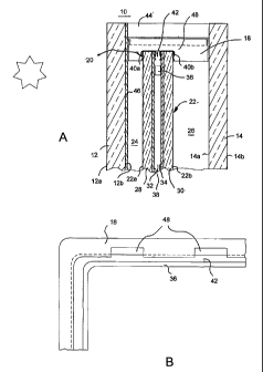
Fig. 1A shows the construction of an electrochromic window assembly 10
according to a first embodiment of the present invention. As shown,
electrochromic
window assembly 10 includes a first transparent substrate 12 and a second
spaced-apart
and parallel second transparent substrate 14. A frame (not shown) may be
provided
about the outer periphery of substrates 12 and 14 and about a portion of the
external
surface 12a of first substrate 12 and the internal surface 14b of second
substrate 14.
Transparent substrates 12 and 14 may be made of tempered glass, annealed,
heat, or
chemically strengthened or laminated glass or other transparent material.
Spacing
between substrates 12 and 14 is maintained by a spacer 18. Spacer 18 may be
made of
wood or aluminum, butyl, EPDM, silicone or other rubbers, steel, or virtually
any,
durable material. Spacer 18 preferably includes a groove 20 for supporting an
electrochromic device 22 in a spaced-apart and parallel position between first
substrate
12 and second substrate 14.
-5-
CA 02416264 2005-06-09
As illustrated with respect to the first embodiment shown in Fig. 1A,
electrochromic device 22 is preferably positioned closer to first substrate 12
than to
second substrate 14. Locating an electrochromic device 22 closer to the outer
substrate
of a window provides the most energy efficient construction. While in later
embodiments it is proposed to integrate the electrochromic device with the
first substrate
such that there is no spacing therebetween so as to maximize energy
efficiency, the first
embodiment includes a first chamber 24 that is defmed between first substrate
12 and
electrochromic device 22. By spacing electrochromic device 22 from first
substrate 12,
resultant chamber 24 may buffer wind loading on electrochromic device 22.
Further,
greater flexibility is achieved in the design and material selection of first
substrate 12 by
not utilizing first substrate 12 as an integral element of electrochromic
device 22. In
other words, first substrate 12 may be made of materials that are otherwise
not suitable
to serve as an integral element of an electrochromic device. For example,
first
substrate 12 may be made of tempered glass or other materials that are not
flat.
A second chamber 26 is similarly provided between electrochromic device 22 and
second inner substrate 14. To provide for thermal insulation, second chamber
26 may
be filled with a gas such as argon. Similarly, first chamber 24 may be filled
with the
same gas or, alternatively, with a different gas. For example, first chamber
24 may be
filled with a gas having a higher thermal conductivity, such as helium, air,
or nitrogen,
which all have higher thermal conductivities than argon, which would
preferably be
provided in the second chamber 26. In this manner, solar energy from the sun
is
absorbed by the electrocbromic device 22 (when in a darkened state), and the
heat that is
generated through this absorpti.on is quickly transmitted via the gas in first
chamber 24
back through first substrate 12 to the exterior of the window and hence
outside the
building. On the other hand, by providing an insulating gas such as argon in
second
chamber 26, the generated heat may be insulated from second substrate 14, and
hence,
the interior of the building. Chamber 24 can also serve as a UV blocking layer
by the
use of a UV absorber. Use of an absorber in solution or in a gel would also
improve
the thermal coupling between the electrochronuc device and the outside.
With respect to the first through fourth embodiments, electrochromic device 22
may have any known construction including, for example, any of the
constructions
disclosed in U.S. Patent No. 6,597,489 entitled ELECTRODE DESIGN
-6-
CA 02416264 2005-06-09
FOR ELECTROCHROMIC DEVICES, filed on June 30, 1999, by Thomas F. Guarr et
al., and U.S. Patent No. 5,805,330.
Preferred alternative constructions are nevertheless described below with
respect
to Figs. 5, 6A-61, 7, and 8.
In general, electrochromic device 22 may include a first transparent element
28,
a second transparent element 30, a first transparent electrode layer 32
applied to an
inward-facing surface of first transparent element 28, a second transparent
electrode 34
applied to an inward-facing surface of second transparent element 30, and a
first seal 36
provided between the two layered transparent substrates. Transparent elements
28 and
30 are maintained in a generally parallel spaced-apart relation. Seal 36
serves to provide
a chamber between elements 28 and 30 in which an electrochromic medium 38 is
contained in contact with both transparent electrodes 32 and 34.
Electrochromic
medium 38 includes electrochromic anodic and cathodic materials that can be
grouped
into the following categories:
(i) Single layer - the electrochromic medium is a single layer of material
which may include small inhomogeneous regions and includes solution-phase
devices
where a material is contained in solution in the ionically conducting
electrolyte and
remains in solution in the electrolyte when electrochemically oxidized or
reduced. U.S.
Patent No. 6,193,912 entitled "NEAR INFRARED-ABSORBING
ELECTROCHROMIC COMPOUNDS AND DEVICES COMPRISING SAME"; U.S.
Patent No. 6,188,505 entitled "COLOR STABILIZED
ELECTROCHROMIC DEVICES"; U.S. Patent No. 6,262,832 entitled
"ANODIC EI.ECTROCHROMIC MATERIAL HAVING A SOLUBLdZING
MOIETY"; U.S. Patent No. 6,137,620 entitled "ELECTROCHROMIC
MEDIA WITH CONCENTRATION ENHANCED STABILITY PROCESS FOR
PREPARATION THEREOF AND USE IN ELECTROCHROMIC DEVICE"; U.S.
Patent No. 6,195,192 entitled "ELECTROCHROMIC MATERIALS
WITH ENHANCED ULTRAVIOLET STABILITY"; U.S. Patent '
No. 6,392,783, entitled "SUBSTITUTED METALLOCENES FOR USE AS AN
ANODIC ELECTROCHROMIC MATERIAL AND ELECTROCHROMIC MEDIA
AND DEVICES COMPRISING SAME"; and U.S. Patent No. 6,249,369
entitled "COUPLED ELECTROCHROMIC COMPOUNDS WITH PHOTOSTABLE
DICATION OXIDATION STATES" disclose anodic and cathodic materials that may be
-7-
CA 02416264 2003-01-15
WO 02/08826 PCT/US01/23182
used in a single layer electrochromic medium. Solution-phase electroactive
materials
may be contained in the continuous solution phase of a cross-linked polymer
matrix in
accordance with the teachings of U.S. Patent No. 5,928,572, entitled "IMPROVED
ELECTROCHROMIC LAYER AND DEVICES COMPRISING SAME" or
International Patent Application No. PCT/US98/05570 entitled "ELECTROCHROMIC
POLYMERIC SOLID FILMS, MANUFACTURING ELECTROCHROMIC DEVICES
USING SUCH SOLID FILMS, AND PROCESSES FOR MAKING SUCH SOLID
FILMS AND DEVICES."
At least three electroactive materials, at least two of which are
electrochromic,
can be combined to give a pre-selected color as described in U.S. Patent No.
6,020,987
entitled "ELECTROCHROMIC MEDIUM CAPABLE OF PRODUCING A PRE-
SELECTED COLOR." This ability to select the color of the electrochromic medium
is
particularly advantageous when designing architectural windows.
The anodic and cathodic materials can be combined or linked by a bridging unit
as described in International Application No. PCT/W097/EP498 entitled
"ELECTROCHROMIC SYSTEM." It is also possible to link anodic materials or
cathodic materials by similar methods. The concepts described in these
applications can
further be combined to yield a variety of electrochromic materials that are
linked.
Additionally, a single layer medium includes the medium where the anodic and
cathodic materials can be incorporated into the polymer matrix as described in
International Application No. PCT/W098/EP3862 entitled "ELECTROCHROMIC
POLYMER SYSTEM," U.S. Patent No. 6,002,511, or International Patent
Application
No. PCT/US98/05570 entitled "ELECTROCHROMIC POLYMERIC SOLID FILMS,
MANUFACTURING ELECTROCHROMIC DEVICES USING SUCH SOLID FILMS,
AND PROCESSES FOR MAKING SUCH SOLID FILMS AND DEVICES."
Also included is a medium where one or more materials in the medium
undergoes a change in phase during the operation of the device, for example, a
deposition system where a material contained in solution in the ionically
conducting
electrolyte which forms a layer, or partial layer on the electronically
conducting
electrode when electrochemically oxidized or reduced.
(ii) Multilayer - the medium is made up in layers and includes at least one
material attached directly to an electronically conducting electrode or
confined in close
proximity thereto which remains attached or confined when electrochemically
oxidized
-8-
CA 02416264 2005-06-09
or reduced. Examples of tliis type of electrochromic medium are the, metal
oxide fil7ms,
such as tungsten oxide, iridium oxide, nickel oxide, and vanadium oxide. A
medium,
which contains one or more organic electrochromic layers, such as
polythiophene,
polyaniline, or polypyrrole attached to the electrode, would also be
considered a
multilayer medium.
In addition, the electrochromic medium may also contain other materials, such
as
light absorbers, light stabilizers, thermal stabilizers, antioxidants,
thickeners, or
viscosity modifiers.
It may be desirable to incorporate a gel into the electrochromic device as
disclosed in commonly assigned U.S. Patent No. 5,940,201 entitled "AN
ELECTROCHROMIC MIRROR WITH TWO THIN GLASS ELEMENTS AND A
GELLED ELECTROCHROMIC MEDIUM," filed on Apri12, 1997.
First and second transparent elements 28 and 30 may be any material which is
transparent and has sufficient strength to be able to operate in the
environmental
conditions to which the device will be exposed. Elements 28 and 30 may
comprise any
type of borosilicate glass, soda lime glass, float glass, or any other
material, such as, for
example, MYLAR , polyvinylidene chloride, polyvinylidene halides, such as
polyvinylidene fluoride, a polymer or plastic, such as cyclic olefin
copolymers like
Topas available from Ticona, LLC of Summit, New Jersey, that is transparent
in the
visible region of the electromagnetic spectrum. Elements 28 and 30 are
preferably made
from sheets of glass.
Additionally, substrates 12 and 14 may be treated or coated as is descn-bed in
U.S. Patent No. 6,239,898 entitled "ELECTROCHROMIC
STRUCTURES," U.S. Patent No. 6,193,378 entitled "AN
ELECTROCHROMIC DEVICE HAVING A SELF-CLEANING HYDROPHILIC
COATING," and U.S. Patent No. 6,816,297 entitled "ELECTROCHROMIC
MIRROR HAVING A SELF-CLEANING HYDROPHILIC COATING," filed
on June 23, 2000. Other treatments, such as anti-reflectance coatings,
hydroph.ilic
coatings, low-E coatings, and UV-blocking layers are also envisioned. Also,
such
coatings may be applied to elements 28 and 30 in this and other embodiments.
Transparent electrodes 32 and 34 may be made of any material which bonds well
to transparent elements 28 and 30, is resistant to corrosion to any materials
within the
electrochromic device, resistant to corrosion by the atmosphere, has minimal
diffuse or
-9-
CA 02416264 2005-06-09
specular reflectance, high light transmission, near neutral coloration, and
good electrical
conductance. Transparent electrodes 32 and 34 may be fluorine-doped tin oxide,
doped
zinc oxide, zinc-doped indium oxide, tin-doped indium oxide (ITO),
ITO/metaUITO
(IMI) as disclosed in "Transparent Conductive Multilayer-Systems for FPD
Applications," by J. Stollenwerk, B. Ocker, K. H. Kretschmer of LEYBOI.D AG,
Alzenau, Germany, the materials described in above-referenced U.S. Patent
No. 5,202,787, such as TEC 20 or TEC 15, available from Libbey-Owens-Ford Co.
of
Toledo, Ohio, or other trausparent conductors. Generally, the conductance of
transparent electrodes 32 and 34 will depend on their thickness and
composition. I1VII
generally has superior conductivity compared with the other materials. I1VII,
however, is
known to undergo more rapid environmental degradation and suffer from
interlayer
delamination. The thickness of the various layers in the I1VII structare may
vary, but
generally the thickness of the first ITO layer ranges from about 10 A to about
200 A, the
metal ranges from about 10 A to about 200 A, and the second layer of ITO
ranges from
about 10 A to about 200 A. If desired, an optional layer or layers of a color
suppression
material may be deposited between transparent electrodes 32 and 34 and the
inner
surface of element 28 to suppress the transmission of any unwanted portions of
the
electromagnetic spectrum.
In the particular embodiment shown in Fig. 1A, seal 36 may be any material
that
is capable of adhesively bonding to the coatings on the inner surfaces of
transparent
elements 28 and 30 to seal the perimeter, such that electrochromic material 38
does not
leak from the chamber defined between the transparent substrates. The seal
preferably
has good adhesion to glass, metals, and metal oxides; preferably has low
permeabilities
for oxygen, moisture vapor, and other detrimental vapors and gasses; and must
not
interact with or poison the electrochromic material it is meant to contain and
protect.
The seal may be applied in any conventional manner. A preferred seal material
and
method for applying the seal as well as a preferred method of constructing
electrochromic device 22 are described further below.
As illustrated in Fig. IA, electrochromic device 22 further includes a pair of
electrical bus clips 40a and 40b that are respectively clipped about the
perimeter of first
and second transparent elements 28 and 30 in such a manner as to physically
and
electrically contact transparent electrodes 32 and 34. Bus clips 40a and 40b
thus enable
electrical current to flow between an external driving circuit through first
and second
-10-
CA 02416264 2005-06-09
. . .
transparent electrodes 32 and 34 and the electrochromic medium 38 contained in
the
chamber therebetween. In this manner, the light transmittance of
electrochromic device
22 may be varied in response to electrical control of an external drive
circuit. Bus clips
40a and 40b may be made of any known construction and known materials. One
possible construction for bus clips 40a and 40b is disclosed in U.S. No.
6,064,509 entitled "AN IMPROVED CLIP FOR USE WITH TRANSPARENT
CONDUCTTVE ELECTRODES IN ELECTROCHROMIC DEVICES" filed on August
22, 1997, by Tonar et al. Preferred constructions for bus clips 40a and 40b,
as well as
preferred materials for the bus clips, are described further below.
Other novel configurations for bus clips would include the use of two bus
clips
that were held together by an insuiating, non-conductive material such as a
plastic or
rubber. This arrangement would allow the bus clips to be attached to both
opposing
glass elements 28 and 30 in one step without allowing them to short each other
out
electrically. See Fig. 6H.
Again, bus clips are used as a means of uniformly transferring electricity
from
lead wires to the conductive coating that has been previously deposited on the
glass
elements. This can also be accomplished by the use of a metal-doped paint or
coating
(such as silver, copper, etc.), or by the use of conductive adhesive tapes,
such as those
available from the 3M Corporation. Examples of these tapes are 3M's
Electrically
Conductive Adhesive Transfer Tape #9703 and #9713. Additionally, metal foil or
exposed wire may be used.
As illustrated in Fig. 1A, a second seal in the form of a sealant 42 is
applied
within any gaps that may exist between the perimeter of electrochromic device
22 and
groove 20. As descrxbed further below, sealant 42 may be an epoxy or the like
that can
readily flow within the small void areas surrounding clips 40 within groove
20.
A third seal in the form of a sealant 44 is also provided between spacer 18
and
first and second substrates 12 and 14 and frame 16. Sealant 44 is provided to
ensure
that the chambers 24 and 26 between substrates 12 and 14 are airtight such
that any
gasses that may be contained in chambers 24 and 26 may not leak out from
between
substrates 12 and 14. Sealant 44 further serves as a moisture barrier for
preventing
moisture from the environment surrounding the window from reaching the
chambers
between substrates 12 and 14.
-11-
CA 02416264 2003-01-15
WO 02/08826 PCT/US01/23182
The sealants 18, 42, and 44 may be a hot melt rubber compound, such as a hot
melt butyl, a silicone, a urethane, a polysulfide, or the like. Additionally,
the sealants
18, 42, and 44 may be modified for aesthetic, chemical, or physical properties
by the
use of various additives. These additives may include, but are not limited to,
anti-
oxidants, pigments, rheology modifiers, fibers, glass and synthetic spheres,
and the like.
The window assembly 10 shown in Fig. 1A may include one or more layers 46
applied to one of the surfaces of substrate 12, substrate 14, and/or either
surface of
electrochromic device 22. Such layers may include a low-emission (low-E) layer
or
stack, a heat mirror, an ultraviolet (UV) filter of blocking layer, and a near
infrared
(NIR) blocking layer or filter.
The placement of the layer 46 will vary, depending on the function it is to
perform. If a UV filter is used, it would be disposed on surface 12a, 12b or
22a in
order to block UV radiation from reaching electrochromic device 22. If the UV
filter is
placed on surface 12a, protection in the form of a hard coat would also be
provided.
Since the electrochromic device would absorb a significant amount of solar
radiation, the
placement of the low-E coating would be somewhat different than commonly used
in
insolated glass units (IGUs) currently available. The electrochromic device 22
in its
darkened state in sunlight would become the portion of the window that has the
highest
temperature, therefore any low-E coatings would be most useful inside of the
electrochromic device 22 to reject heat during the summer months. The low-E
coating
would be disposed on surfaces 22b, 14a, or 14b, with 22b giving the best
rejection of
heat from the outside, again if surface 14b is coated with a low-E coating, an
additional
hardcoat could also be provided. The NIR filter, if it absorbs NIR radiation,
would be
heated by sunlight and for heat rejection would preferably be placed on one of
the
surfaces of substrate 12 or on surface 22a. Additionally, if the low-E coating
were
disposed on substrate 14, an NIR absorbing filter could be placed on surface
22b.
As illustrated in Figs. 1A and 1B, window assembly 10 may further include one
or more channels 48 formed in spacer 18 that extend from one side of
electrochromic
device 22 to the other side and thereby allow airflow between first chamber 24
and
second chamber 26. By allowing such airflow between the chambers, the affects
of
wind loading on device 22 may be reduced. Such wind loading causes substrate
12 to
bow inward, causes the gas contained in a airtight chamber 24 to compress, and
thereby
causes electrochromic device 22 to also be affected by wind loading.
Channel(s) 48
-12-
CA 02416264 2005-06-09
equalize the pressures on either side of electrochromic device 22 and thereby
reduces
any flexing of the transparent substrates or other components of
electrochromic device
22 as a result of wind loading. Such air passage between channels 24 and 26
also would
reduce temperature loading that may otherwise occur, which would again cause
an
increase of pressure in the gas in the first chamber 24 without otherwise
producing an
equal increasing pressure in second chamber 26. Clearly, if different gasses
are
maintained in chambers 24 and 26, one would not utilize channel(s) 48.
As shown in Fig. 1A, first seal 36 is protected from the environment outside
of
the window by second sea142, spacer 18, third sea144, and frame 16. The
sealant used
to form third sea144 is preferably highly resistant to air and moisture such
that the space
between substrates 12 and 14 is completely airtight. When chambers 24 and 26
are
filled with an inert gas such as argon, the materiai selected for first seal
36 and second
seal 42 need not be oxygen impermeable or even moisture impermeable.
Nevertheless,
first sea136 must not interact with or poison the electrochromic medium 38. By
removing the requirements that first sea136 need be oxygen and moisture
impermeable,
seal 36 may be constructed using materials not currently used in the
construction of
electrochromic devices. That is, since the inner most ("primary") seal
essentially need
only contain the electrochromic fluid or gel, whereas the secondary seal is
more
importaxrtly an oxygen and moisture vapor barrier, the material out of which
the inner
most seal is constructed can be selected from a wide range of materials. This
allows the
primary seal to be made out of less expensive materials. These materials can
be
polyisoprene, polyisobutylene, polychloroprene, ethylene propylene diene
methylene
rubbers, polyetheylenes, flurorcarbon rubbers, silicone rubbers, epoxies,
polyurethanes,
nitriles, butyl rubber, neoprene, Teflon (tetrafluoroethylene fluorocarbon,
fluorinated
ethylene-propylene, or copolymers thereof) and the like. Additionally, these
materials
may be modified with different additives to affect the chemical, physical, or
their
aesthetic appearance. For example, black pigments could be used to produce a
dark
sealant, and fumed silica could be used to increase thixotropy or adjust the
CTE, such as
is described in U.S. Patent No. 6,157,480, filed on September 21, 1998.
The epoxy seals currently used in constructing electrochromic mirrors are
often
thermally cured epoxies. Because electrochromic windows are much larger than
the
rearview mirror, the therrnal energy that would be required to thermally cure
the epoxy
would be extremely large. Also, the epoxy seals previously used are relatively
brittle
-13-
CA 02416264 2003-01-15
WO 02/08826 PCT/US01/23182
after curing. Additionally, while such an epoxy works well for smaller
electrochromic
devices, such as electrochromic rearview mirrors for automobiles, when such an
epoxy
is used for larger scale electrochromic devices such as windows, there is
great difficulty
in maintaining the two transparent elements 28 and 30 in a parallel spaced-
apart relation
throughout the entire surface area of the electrochromic device, particularly
when the
epoxy is not firm enough to maintain the spacing until it has time to cure.
Because seal
36 is sufficiently protected from the external environment and would only be
exposed to
the electrochromic medium 38 and an inert gas between substrates 12 and 14,
first seal
36 may be made of a material that need not be cured, such as a butyl rubber,
silicone,
EPDM, polyisobutylene, Teflon, neoprene, viton, or the like. Thus, first seal
36 may
serve as a spacer both during and after the manufacture of the electrochromic
device.
Because seal 36 may be made with a stable material, the manner in which such
an
electrochromic device is manufactured may be advantageously modified as
discussed
further below and thereby provide for a much simpler and inexpensive method of
manufacture that further facilitates mass-production of such large-scale
electrochromic
devices.
Fig. 2A shows an electrochromic window assembly 100 constructed in
accordance with a second embodiment of the present invention. As will be
apparent to
those skilled in the art, the second embodiment is similar to the first
embodiment with
the exception that electrochromic device 22 is disposed between two separate
spacers
118a and 118b. Such a construction still allows for the provision of the
electrochromic
device 22 within an airtight chamber between substrates 12 and 14. One
advantage to
this construction is that it allows for the seal and spacer region around the
periphery of
the window unit to have a lower profile than in the construction shown in Fig.
lA. Fig.
2B shows a modified version of the second embodiment wherein spacers 118a and
118b
are replaced with a single spacer 18 and wherein the bottom edges of spacer 18
is
tapered so as to hide seal 36.
Fig. 3A shows an electrochromic window construction 120 according to a third
embodiment of the present invention. Window 120 differs from the windows of
the
previous embodiments in that the electrochromic device is formed adjacent
first substrate
12 with no chamber formed therebetween. Nevertheless, a chamber is still
provided
between electrochromic device 22 and the inside second substrate 14 that may
be an
airtight chamber filled with an insulating gas such as argon or the like.
Window
-14-
CA 02416264 2003-01-15
WO 02/08826 PCT/US01/23182
construction 120 further may differ from the -prior embodiments by eliminating
first
transparent element 28 and instead applying first transparent electrode 32 on
a surface of
first transparent substrate 12. By eliminating transparent element 28 and by
positioning
the electrochromic medium 38 closer to external substrate 12, the window
assembly is
not only lighter and less complex, but the heat rejection of this construction
is enhanced.
If preassembly of the electrochromic device 22 is desired, a thin transparent
sheet of
glass, Mylar, or another plastic material may be used as a first transparent
element 28
and subsequently adhered to the surface of transparent substrate 12. Such a
thin
transparent sheet could also be used for element 30. The layer 46 in this
embodiment
would have similar placement with surface 12b and 22a acting as if they had
been
merged into a single surface.
To make electrical connection with the two transparent electrodes 32 and 34,
an
electrically conductive bus clip 40b may be utilized to contact second
transparent
electrode 34 while electrical contact may be made with first transparent
electrode 32 by
means of an electrical conductor 122 in the form of an exposed wire or metal
foil.
Conductor 122 may be pressed against first transparent electrode 32 outside of
first seal
36 and then covered with the insulated glass unit spacer 124. Alternatively,
as shown in
Figs. 7 and 8, the electrical conductor may be disposed between first seal 36
and
transparent electrode 32. Further still, as shown in Fig. 3B, transparent
electrode 32
may extend up beyond third seal 44 where contact is made with a conductive
clip 122b
on the outside of the airtight chamber formed between substrates 12 and 14.
As illustrated in Fig. 3A, seal 36 is still advantageously maintained within
the
airtight chamber between substrates 12 and 14 that is formed by spacer 124 and
seal 44.
Accordingly, seal 36 may be made with materials that facilitate simple and
inexpensive
manufacture of the electrochromic device. Again, material requirements are
much less
due to seal 44.
Fig. 4A shows an electrochromic window assembly 140 constructed in
accordance with a fourth embodiment of the present invention. The embodirnent
shown
in Fig. 4A differs from the prior embodiments in that one or more additional
electrooptic
device(s) 142 is/are provided within the airtight chamber defined between
substrates 12
and 14. First electrochromic device 22 is preferably positioned as close as
possible or
on the inward-facing surface 12b of first substrate 12 while second electro-
optic device
142, which may be another electrochromic device, or a polymer dispersed liquid
crystal
-15-
CA 02416264 2003-01-15
WO 02/08826 PCT/US01/23182
or suspended particle device (SPD), is positioned closer to the second
substrate 14. If
device 22 and 142 are to be formed on the respective surfaces 12b and 14a of
substrates
12 and 14, then the construction of Figs. 3A and 3B may be utilized in tandem
for the
construction shown in Figs. 4A and 4B. On the other hand, if one or more of
the
devices 22, 142 are spaced apart slightly from the respective substrates 12
and 14 so as
to define respective chambers 144 and 148, gasses having a high thermal
conductivity
may be contained within chambers 144 and 148 so as to facilitate the transfer
of heat
from the electrochromic devices to the outside of the inner window chamber
146.
Chamber 146 would then preferably be filled with an inert insulating gas such
as argon.
Chamber 146 may also be filled with an inert solvent or a free-standing gel.
For some window applications, it may be desirable to combine the features of
electrochromic technology with another technology such as Polymer Dispersed
Liquid
Crystal (PDLC) technology. The electrochromic systems typically used for
windows are
good for attenuating light (and heat) transmission, but the transition times
between the
high and low transmission states are typically measured in minutes not
seconds. The
transmitted image in the low transmission state is typically clear and free of
haze and
distortion. These are great attributes for a window system except if complete
privacy is
desired. A PDLC window system changes from a relatively clear transmissive
state to a
light scattering cloudy or opaque state. The transmission times from clear to
opaque are
measured in seconds not minutes. If privacy is desired, the attributes of a
PDLC may be
preferred, but since the PDLC window just scatters light in the opaque state,
it is very
poor at attenuating the total amount of light (and heat) that is transmitted
through the
window. If privacy and light and heat attenuation is desired, it is preferred
to combine
the two technologies. A PDLC film constructed in a conventional manner could
be
laminated to an electrochromic window device or the devices could share a
substrate in a
three-substrate device (substrate/electrochromic layer/substrate/PDLC
layer/substrate).
The PDLC and electrochromic layers could be operated separately or
simultaneously.
The PDLC layer could be oriented in front of the electrochromic layer such
that it first
scatters the direct sunlight which is then absorbed by the electrochromic
layer or the
electrochromic layer could be oriented first. The PDLC layer may contain an UV
absorber to protect the electrochromic layer if it is oriented closer to
substrate 12.
By providing a second electrochromic or electro-optic device closer to the
inside
substrate 14 of window assembly 140, heat from the incident solar energy may
be
-16-
CA 02416264 2003-01-15
WO 02/08826 PCT/US01/23182
transmitted to the inside of the house rather than the outside of the house
during winter
months and colder days whereas heat can be rejected by utilizing
electrochromic device
22 during the summer months and warmer days. Optionally, the two devices can
attenuate different wavelengths of light, for example, visible and NIR.
Further, one of
the two devices 22 and 142 could be used at any one time. Nevertheless, it
would also
be possible to simultaneously activate both devices 22 and 142, particularly
during
summer months, to provide additional absorption of solar light that would
otherwise be
transmitted through the structure. Such simultaneous activation may also be
desired at
nighttime for purposes of added privacy. The placement of the layer 46 in this
embodiment will be somewhat different than has been discussed previously. If
an UV
filter or NIR absorbing layer is used, it again would be disposed on surface
12a, 12b, or
22a in order to block radiation. The placement of the low-E coating would be
somewhat
different than in the previous discussion since the construction of Fig. 4A is
designed to
enhance the heat retained inside the building during the winter months and
colder days.
The low-E coating would be disposed on surfaces 22b or 142a to reject the heat
from the
outside during the cooling seasons and to retain heat during the heating
seasons.
Fig. 4B shows a variation of the spacer construction for a dual-element window
in which spacer 124 extends across the tops of elements 22 and 142 rather than
in
between elements 22 and 142 as in the construction shown in Fig. 4A.
As discussed above, a benefit of maintaining the electrochromic device within
the
airtight chamber of the insulated glass unit is that a first seal 36 (206 in
Figs. 5 and 6A-
61) need not be highly impermeable to oxygen and moisture, and need not be
further
cured after original manufacture of the electrochromic device. An example of a
preferred material is EPDM that may be preformed as a gasket that is
subsequently
adhered to the surface of a transparent substrate 202 (see Figs. 5 and 6A).
Transparent
substrate 202 is coated with a transparent electrode 204. In addition, an
adhesive may
be applied in advance to the opposite surface of seal 206 and a release liner
208 may be
applied to the adhesive such that the subassembly 200 shown in Fig. 5 may be
preassembled and stored in inventory. Previously, such a preassembled
subassembly for
an electrochromic device could not be constructed due to the materials that
were
required to be used for the seal.
It should be noted that the drawings discussed above and below are not to
scale,
but have exaggerated dimensions in some respects, particularly in their
thicknesses, to
-17-
CA 02416264 2003-01-15
WO 02/08826 PCT/US01/23182
illustrate the principles of the invention. It should be understood that
certain aspects of
the invention may be applied to smaller electrochromic devices, such as
electrochromic
rearview mirrors.
The inventive method for constructing an electrochromic device of the type
that
may be implemented in a large electrochromic window assembly is discussed
below with
reference to Figs 6A-61. As illustrated in Fig. 6A, a subassembly 200 (see
also Fig. 5)
is constructed whereby a seal gasket 206 is adhesively attached or bonded to
the surface
of a transparent electrode layer 204 that is formed on a transparent substrate
202.
Transparent glass substrates having a preapplied layer of a transparent
electrode are
commercially available, such as TEC-15 glass from Libbey-Owens-Ford. As
illustrated
in Fig. 6A, a release liner 208, such as polyethylene or siliconized polyester
or the like,
may be applied to the opposite surface of seal gasket 206. Release liner 208
could be
secured to seal gasket 206 by the same adhesive that would subsequently be
used to
secure a second transparent substrate 210 having a transparent electrode layer
212
formed thereon (see Fig. 6B).
Conceivably, seal gasket 206 could be preconstructed to have adhesive applied
to
its two opposite surfaces and release liners may be applied to both surfaces
of seal gasket
206. This would allow the seal gaskets by themselves to be separately stored,
then
selected and readily applied onto one of the coated substrates 202 or 210.
Because seal
gasket 206 has sufficient resistance to compression to maintain cell spacing
while
extending around substantially the entire periphery of the transparent
substrates, seal
gasket 206 functions as a spacer both during and after the manufacturing
process.
As shown in Fig. 6B, once release liner 208 has been removed from seal gasket
206, a second subassembly 213 including a second transparent substrate 210,
having one
surface coated with a transparent electrically conductive materia1212, may be
aligned
with transparent substrate 202 and pressed into contact with the adhesive on
seal gasket
206. This operation may be performed with substrates 210 and 202 disposed in
either
horizontal planes or vertical planes. An apparatus such as a vacuum chuck or
the like
may be used to move substrates 212 and 202 together. Once coated .substrates
202 and
210 are pressed into contact via seal gasket 206, a secondary seal may be
applied and the
chamber defined between coated substrates 202 and 210 and seal gasket 206 may
be
filled with an electrochromic medium 215. Preferably, the electrochromic
medium
contains a gelling agent that will form a cross-linked polymer matrix between
coated
-18-
CA 02416264 2003-01-15
WO 02/08826 PCT/US01/23182
substrates 202 and 210. Substrates 202 and 210 may be held in place by the
vacuum
chuck that first holds the substrates in a fixed position until the chamber is
filled with
the electrochromic medium. Once the matrix has been formed, the assembly will
exhibit
sufficient structural integrity such that one of the substrates will not bow
towards the
other substrate in a middle portion of the device and the spacing between the
substrates
will be maintained uniform throughout the device.
Additionally, the first seal may be dispensed and include various rheology
modifiers to adjust the flow characteristics of the dispensed material. Other
additives
could be used to affect other chemical, physical, or aesthetic properties. To
maintain the
desired cell spacing when a dispensed material is employed, the spaced apart
relationship
of the substrates 28 and 30 could be maintained by the use of certain spacers
consisting
of, for example, glass spheres, synthetic spheres, rubber blocks, and the
like.
As shown in Fig. 6C, coated substrate 210 preferably includes a fill hole 214
into
which the electrochromic material is introduced. An additional aperture (not
shown)
may also be formed to enable a vacuum to be attached and hence to allow vacuum
enhanced filling of the chamber between the two substrates. The fill hole 214
is
preferably conically shaped with the larger opening disposed at the exterior
of the
device. The conical hole is formed by drilling partially from each side of the
glass lite
to avoid the uneven breakthrough and shattering seen when such a hole is
drilled from
one side only. After the introduction of electrochromic material into the
device, the fill
hole(s) is plugged (sealed) with some type of material that will not adversely
affect the
electrochromic material. This material may be a polymeric material such as
polyisobutylene, polyolefin, butylnitrileand the like. Alternatively, this
material may be
a pliable or rigid sphere or spheroid whose size is selected to fit within the
conical hole
without dropping into the space formed by the two spaced-apart glass elements.
This
sphere or spheroid may be made of glass, Teflon (tetrafluoroethylene
fluorocarbon,
fluorinated ethylene-propylene, or copolymers thereof), or the like.
Preferably, the
sphere is a Teflon ball obtained from Small Parts Inc. The material utilized
as the
conical hole sealant may also be held in place by an adhesive material. This
material
may be a pressure sensitive adhesive or a UV curable material, preferably
Dyamx
20014. A glass or plastic slide may also be superimposed upon the adhesive as
an
additional sealing material. In the case of a UV curable adhesive, the slide
is positioned
over the plugged conical hole prior to the curing of the adhesive.
-19-
CA 02416264 2003-01-15
WO 02/08826 PCT/US01/23182
During filling, the structure shown in Fig. 6C may be rotated from a vertical
orientation with fill hole 214 at the top portion of the structure so as to
use gravity to aid
filling, to a horizontal position. Rotation about another axis simultaneously
is also
possible. This prevents air bubbles from getting trapped in the chamber. By
forming
fill hole 214 in a conical shape, a ball 216 may subsequently be inserted into
fill hole
214 after filling has been completed (see Fig. 6D). The chosen shape of fill
hole 214
serves to prevent plug 216 from falling through substrate 210 into chamber 215
and
allows for the plug to have a preformed shape, such as spherical, conical,
etc. Again,
the dimensions of fill hole 214 and ball 216 relative to the electrochromic
device
structure shown in the figures is exaggerated for purposes of illustration. In
general, fill
hole 214 and ball 216 would be extremely small when compared to the entire
surface
area of the electrochromic device.
Fill hole 214 is preferably formed near the perimeter of the electrochromic
device in an area just lying inside of the sealed area of the chamber. In this
manner, the
fill hole and plug will not be highly visible to someone looking through the
window and
may be obscured by the frame or spacer used to hold the electrochromic device
within
the window structure.
Plug 216 is preferably made of a material that will not poison or interact
with the
electrochromic medium contained in chamber 215. More specifically, plug 216 is
preferably spherical in shape and made of materials such that when the plug is
inserted
in hole 214, it snuggly fits within fill hole 214. Plug 216 may be made of
polyethylene,
Teflon , stainless steel, gold, glass, ceramic, polypropylene, polyamide, PIB,
butyl
rubber or EPDM. As shown in Fig. 6E, after plug 216 has been inserted into
fill hole
214, an adhesive 218 is applied to the top of plug 216 so as to slightly
overfill fill hole
214. Preferably, UV curable adhesive is Dymax 20014. By utilizing a plug 216
or any
other similar structure that could fill a fill hole of virtually the same
shape in a similar
manner, adhesive 218 is prevented from coming into contact with the
electrochromic
material disposed within chamber 215. This is important, since many of the
adhesives
interact with, or otherwise poison, electrochromic materials that are commonly
used for
electrochromic devices. Subsequently, a thin transparent member 220 is pressed
down
onto adhesive 218 until it essentially lies flat on the outer surface of
coated substrate 210
as illustrated in Fig. 6F. Member 220 is preferably made of a material that is
transparent to UV radiation and that is also impermeable to oxygen. Member 220
may
-20-
CA 02416264 2003-01-15
WO 02/08826 PCT/US01/23182
be made of Mylar or a glass microscope slide slip cover. Member 220 is
preferably
dimensioned to be sufficiently larger than the opening of fill hole 214 so as
to increase
the path that oxygen or moisture would need to travel to enter the device
through fill
hole 214.
Then, as illustrated in Fig. 6F, UV radiation 222 is directed onto and through
member 220 so as to cure adhesive 218. Once adhesive 218 has cured, a very
strong
plug for fill hole 214 is created without utilizing any highly visible plug
for the fill hole.
Fig. 6G shows the next step in the process, which is to apply bus clips 40a
and
40b to coated substrates 210 and 202. Such clips are generally friction fit
around the
perimeter of the electrochromic device.
In prior constructions, particularly in electrochromic devices used as
rearview
mirrors, two separate bus clips were typically applied along opposite edges of
the
electrochromic device so as to avoid inadvertent contact and electrical
shorting between
the bus clips. Thus, for example, prior electrochromic devices would include
bus clips
positioned such as in location 41a and 41b shown in Fig. 6G with substrates
210 and 202
offset from each other. Furthermore, such bus clips would only extend along a
top or
bottom edge of the electrochromic device, since the distance through which the
current
would flow was not excessively great. With larger scale electrochromic devices
such as
those used in windows, the distance between the bus clips and the opposite
edge of the
corresponding transparent electrode tends to cause non-uniform current flow
through the
transparent electrodes. Such non-uniform current flow causes non-uniform
coloration of
the electrochromic material, which can be aesthetically undesirable.
Previously, bus clips were conventionally formed of a metal strip or spine
with a
plurality of resilient fingers extending transversely from the spine. As an
example, with
reference to Fig. 611, conventional bus clips included a spine 230a and a
plurality of
spaced-apart resilient fingers 226a and 228a that extend transversely from the
spine. As
shown in Fig. 6G, such clips would have fingers that are tapered slightly
inward so as to
clamp onto the outer periphery of the coated substrates. In general, in
conventional bus
clips, fingers 226a and 228a had widths that were much greater than the
spacings
between each of the fingers. Thus, the fingers extending from a conventional
spine 230a
had the same appearance on both sides thereof as fingers 226a shown in Fig.
6Ii. The
inventive bus clips, on the other hand, differ from the conventional bus clips
insofar as
every other finger on at least one of the sides of the bus clip is removed or
otherwise not
-21-
CA 02416264 2003-01-15
WO 02/08826 PCT/US01/23182
provided so as to allow a bus clip on the other substrate to be applied along
the same
edges without making physical or electrical contact with the fingers of the
other bus clip.
Thus, the fingers have widths that are less than the spacing therebetween to
allow the
fingers of the two bus clips 40a and 40b to be effectively intermeshed at
least in those
regions where the fingers of opposing bus clips extend towards one another.
As shown in Figs. 10A and lOB, the spacing or pitch between fingers 228 should
be greater than the width of fingers 228 themselves to allow for bending the
bus clip
around the corners of the substrates without inadvertent contact that would
cause a short.
Likewise the length of the fingers should be selected to also prevent such
shorting. As
shown in Fig. lOC, fingers 226 and 228 may have dimples 400 so as to provide
better
electrical contact with the transparent electrodes.
By utilizing the inventive bus clip structure shown in Figs. 6H, 10A, and lOB,
bus clips may be provided about the entire periphery of both coated
transparent
substrates 210 and 202 without making physical contact with one another. Thus,
by
enabling bus clips to be provided around the entire periphery of the
electrochromic
device and hence contact the respective transparent electrodes 204 and 212
about their
entire perimeters, the transparent electrodes will show a more uniform current
density
throughout the surface of the electrochromic device and the electrochromic
medium will
color more uniformly to its darkened state and be less prone to segregation
than prior
configurations. To ensure that the bus clips do not slide along the edge of
the substrates
and come into contact with one another, and to provide a second seal that may
have
better moisture and oxygen impermeability properties, an epoxy sealant (not
shown)
may be applied to the outer perimeter of the electrochromic device . This
epoxy sealant
may be applied prior to filling of the window or it may be applied at the time
during
which the electrochromic device is secured within a groove of an insulated
glass spacer
member or between spacer members.
Another advantage of the inventive construction is that bus clips 40a and 40b
may
be constructed of materials previously not considered suitable for an
electrochromic
device. In particular, steel or other iron containing elements were not
previously
considered for use as bus clips due to the fact that such materials will rust
as a result of
surface oxidation when exposed to oxygen. However, by protecting the entire
electrochromic device structure within an airtight chamber between the two
substrates of
the insulated glass assembly, and by further filling the chambers with inert
gas such as
-22-
CA 02416264 2003-01-15
WO 02/08826 PCT/US01/23182
argon, bus clips made of steel or the like will not be exposed to oxygen and
will thus not
rust. Steel clips are preferable to conventional clip materials, since they
are roughly
one-fifth of the cost. Because it is preferable to extend the bus clips around
the entire
periphery of the electrochromic device, this cost savings is all the more
significant.
Fig. 7 shows an alternative construction for extending electrical conductors
in
contact with the respective transparent electrodes 204 and 212 about their
entire
perimeter. Specifically, in Fig. 7, two exposed wires 235a and 235b are
pressed into
opposite sides of seal gasket 206. The adhesive that is applied to the seal
gasket serves
to hold the wires in place as the wires are extended around the perimeter of
seal gasket
206. This assembly may then be adhered and pressed against the respective
transparent
electrodes 204 and 212, and thereby provide contact with electrical wires 235a
and 235b
about the entire perimeter of electrodes 204 and 212. A similar approach shown
in Fig.
8 may be taken using conductive foil strips 240a and 240b that may be adhered
to
opposite sides of seal gasket 206. A conductive adhesive layer could then be
applied to
the exposed surfaces of the metal foil to adhere to transparent electrodes 204
and 212.
The conductive foil strips could be applied on the inside or outside of the
transparent
elements and also could be applied by vacuum depositing a conductive metal
around the
perimeter of the device.
It should be noted that while the manufacturing method discussed above is
described with respect to electrochromic devices for incorporation into
windows, such a
method may be applied to electrochromic devices or even other devices
providing
variable light transmittance. For example, such a method could be used to
construct
electrochromic rearview mirrors. Further, the inventive fill hole and plugging
structure
may also be utilized in an electrochromic mirror as may the inventive bus clip
construction described above. Further, while specific window assemblies are
described
above with respect to Figs. 1-4, the inventive electrochromic device may be
incorporated
into any other known window structure.
It should also be noted that a photovoltaic power source may additionally be
added to the above window structures as disclosed in U.S. Patent No.
5,805,330. The
photovoltaic source may be used to power the electrochromic device.
Fig. 9 shows an embodiment of the window assembly that includes a control
mechanism for monitoring the light levels transmitted through electrochromic
device 22
and for adjusting the voltage level applied to electrochrornic device 22 so as
to vary its
-23-
CA 02416264 2005-06-09
transmittance and thereby maintain a constant level of light in the interior
of the
building. This system includes a photo sensor 300 that may be a part of a
photovoltaic
power source that is mounted within chamber 26 behind electrocb.romic device
22. By
mounting photo sensor 300 behind electrochromic device 22, the sensor may
sense the
light level as attenuated by electrochromic device 22 and thereby adjust its
transmittance/absorption characteristics so as to maintain a uniform intensity
of light as
sensed by the sensor. The circuitry for controlling the voltage applied to
electrochromic
device 22 may also be incorporated within chamber 22 or otherwise incorporated
within
the frame/spacer assembly. If photosensor 300 is part of a photovoltaic power
supply,
then the voltage that is to be supplied to electrochromic device 22 may be
generated
from within the window assembly itself.
As also shown in Fig. 9, a manual switch mechanism 302 may be supplied on the
outside of transparent substrate 14 that allows a person to effectively dial
the desired
transmittance level. Switch 302 may supply this signal to the circuitry and to
photosensor 300 via a magnetic link through glass 14 in a similar manner to
which
signals are transmitted through automotive glass in cellular telephone
antennas. The
transmittance level of electrochromic device 22 may also be controlled
remotely using a
wireless receiver that is contained within chamber 26. The wireless receiver
may be an
infrared sensing photodiode or the like so as to receive an infrared control
signal from a
remote transmitter. The receiver may also be a radio frequency receiver. In
this
manner, the transmittance levels of the windows may be remotely controlled
using a
remote control transmitter. Also, the transmittance of the windows may be
adjusted
under control of a microprocessor-based system remote from the windows that
may send
control signals via an X10-type system through the commercial power lines of
the
building in which the windows are mounted.
A preferred electrical control system and electrical contacts for coupling the
electrochromic window to the electrical control system is disclosed in
commonly-
assigned published International Application No. WO 02/09338 entitled "SYSTEM
TO
INTERCONNECT, LINK, AND CONTROL VARIABLE TRANSMISSION
WINDOWS AND VARIABLE TRANSMISSION WINDOW CONSTRUCTIONS,"
filed on July 12, 2001.
As noted above, color instability has been a drawback of prior art
electrochromic
windows. That is, when these windows have been exposed to outdoor weathering
-24-
CA 02416264 2003-01-15
WO 02/08826 PCT/US01/23182
conditions, high temperatures, and UV radiation, for extended periods of time
in both
their inactivated and activated states, or cycled, unacceptable changes in the
color of
these windows have occurred. Additionally, accelerated testing for
electrochromic
windows to predict the field life of a device in a relatively short period of
time, has
generally used the change in absorbance at a given wavelength, or the percent
of white
light transmitted as a figure of merit in evaluating electrochromic devices
after a series
of tests. These values, while being easily measured, may not be related to
consumer
acceptability, that is, a small change in the absorbance at a chosen
wavelength does not
give any information about changes at any other wavelength. Also, the use of
percent
light transmission may be similarly misleading or incomplete as an indication
of the
acceptability of an electrochromic window. The change in the value of color
coordinates
as a figure of merit is more useful in evaluating electrochromic windows than
the
methods previously used. Also, this measured color change is a more sensitive
measure
of perceived appearance than either percent light transmission or absorbance
change at a
given wavelength. .
In accordance with the present invention, electrochromic devices are disclosed
that exhibit superior color stability, in addition, a straightforward,
relatively short time
test methods for evaluating various electrochromic device designs and
constructions for
suitability are disclosed.
First, an electrochromic device to be evaluated is constructed using the
combination of materials, solvents, polymerizing agents, etc. desired. After
construction, the light transmitted through an electrochromic device is
measured and
recorded in the L*a*b* color space. The device is then exposed to simulated
sunlight
conditions in a weathering chamber for a period of at least 600 to 700 hours
while
cycling between its high transmittance state and its low transmittance state,
being held in
its low transmittance state for at least 30 percent of the total exposure
time. After the
exposure, the color of the transmitted light is again measured and the
difference between
the color coordinates for both the clear and colored state are calculated. It
has been
found that devices that have a color change of less than five after this
exposure exhibit
enhanced color stability when exposed to outdoor weather conditions after
prolonged
periods, greater than two years.
Second, a device after fabrication, is cycled while exposed to an elevated
temperature of 85 C for a period of 1000 hours, the color coordinates are also
recorded
-25-
CA 02416264 2003-01-15
WO 02/08826 PCT/US01/23182
before and after this exposure. In this case also, a color change of five or
less is
indicative of the capability of similarly constructed devices to withstand
prolonged
outdoor exposure. The use of ten as an upper limit for the color change in
evaluating
electrochromic windows may seem arbitrary, however, after evaluation of a
number of
windows, it is believed that this color change is approximately the limit for
customer
acceptance for aging of electrochromic windows. That is, if a window were
required to
be replaced due to breakage, or for some other reason, the replacement window
would
be similar in appearance to the aged windows. A color change of five or less
is believed
to be required for broad customer acceptance of the difference between an aged
window
and a new one. More preferably, a color change of one or less will generally
give aged
windows whose color is generally indistinguishable from a new window by people
with
normal color vision.
In the above discussion and the following examples, references are made to the
spectral properties of electrochromic windows constructed in accordance with
the
parameters specified in each of the examples. In discussing colors, it is
useful to refer
to the Commission Internationale de I'Eclairage's (CIE) 1976 CIELAB
Chromaticity
Diagram (commonly referred to as the L*a*b* chart). The technology of color is
relatively complex, but a fairly comprehensive discussion is given by F.W.
Billmeyer
and M. Saltzman in Principles of Color Technology, 2nd Edition, J. Wiley and
Sons Inc.
(1981), and the present disclosure, as it relates to color technology and
terminology,
generally follows that discussion. In the L*a*b* space, L* defines lightness
with an L*
value of 100 being white and a L* value of 0 being black, a* denotes the
red/green value
with a positive a* indicating red and a negative a* indicating green, and b*
denotes the
yellow/blue value with a positive b* indicating yellow and a negative b*
indicating blue.
Each of the electrochromic media has an absorption spectra at each particular
voltage
from which the L*a*b* values may be calculated. To calculate a set of color
coordinates, such as L*a*b* values, from the spectral transmission or
reflectance, two
additional items are required. One is the spectral power distribution of the
source or
illuminant. The present disclosure uses CIE Standard Illuminant D65. The
second item
needed is the spectral response of the observer. The present disclosure uses
the 2-degree
CIE standard observer. The illuminant/observer combination used is represented
as
D65/2 degree. The value AE is equal to the square root of (Lf*-Lt*)Z (a.t*-ai
*)2+(bf*-
bi *)2 where the "i" subscript denotes the initial values of the color
coordinate values and
-26-
CA 02416264 2003-01-15
WO 02/08826 PCT/US01/23182
the "f' subscript denotes the color coordinate values after testing, and
hence, provides a
measure for quantifying color stability. For an electrochromic window color
stability,
the AE value of the window should be less than 10. Preferably, the DE value is
less
than 5, and more preferably is less than about 1.
To illustrate the properties and advantages of the present invention, examples
are
provided below. The following illustrative examples are not intended to limit
the scope
of the present invention, but to illustrate its application and use. In the
examples below,
each of the electrochromic windows was constructed in the same conventional
manner.
Specifically, two pieces of glass coated with a transparent conductive coating
(TEC-15
glass from Libbey-Owens-Ford) were held in a spaced-apart relationship with an
epoxy
seal material containing glass beads with 250 mm diameter. A gap was left in
the seal
for the introduction of the electrochromic medium into the cell via vacuum
backfilling.
The gap was plugged with a UV-curable material after backfilling.
Specifically, 2 by 5 windows refer to devices constructed with two pieces of
glass
each approximately 2 inches by 5 inches coated with a transparent conductive
coating
(unless otherwise noted TEC-15 glass from Libbey-Owens-Ford) were held in a
spaced-
apart relationship with a seal material containing spacers, for example, glass
beads with
a specific diameter. A gap was left in the seal for the introduction of the
electrochromic
medium into the device via vacuum backfilling. The gap was then plugged.
Example 1
Two of the above constructed windows were filled with a solution containing
16mM dimethyl-4,4'-bipyridinium bis(tetrafluoroborate); 16mM 5,10-dihydro-5,10-
dimethyl phenazine and 30mM 4'-methyl-2'-hydroxy-phenyl-benzotriazole (Tinuvin
P)
in propylene carbonate (PC) with 3 wt% polymethyl methacryate (PMMA). The
color
coordinates (L*a*b* D65/2 ) of transmitted light were recorded and the windows
were
then subjected to 730 hours of high intensity UV light in an Atlas Weather-
Ometer with
an Xe lamp operating at 0.55W/m2 at 340nm (a darkening cycle consisting of
operation
of the device at 1.2V for 20 sec. and at 0. OV for 40 sec., these times
allowed for the
devices to undergo darkening to their steady state transmission values and
allow the
devices to clear-completely). The color coordinates were again recorded and
the
difference (AE) for the windows in their high transmission condition was 2.50
and 2.22
for the low transmission condition AE was 4.45 and 4.99.
Example 2
-27-
CA 02416264 2003-01-15
WO 02/08826 PCT/US01/23182
Two windows were constructed the same as in Example 1, but were filled with
16mM bis (2-phenyl ethyl)-4,4'-bipyridinium bis (tetrafloroborate) 16mM DMP,
30
mM Tinuvin P in PC with 3wt% PMMA. A similar test as performed to Example 1
was
performed except that the windows were measured after 629 hours. These windows
exhibited a AE (high transmission) of 1.18 and 1.121 and a AE (low
transmission) of
1.09 and 1.33.
Example 3
Two windows were constructed having the same structure as in Examples 1 and 2
above except that the windows were filled with 15mM bis (3-phenyl propyl)-4,4'-
bipyridinium bis (tetrafluoroborate), 16mM DMP 30mM Tinuvin P in PC with 3wt%
PMMA after 629 hours, which is a conventional electrochromic material.
Accordingly,
this example served as a control for purposes of comparison with Examples 1
and 2
above. The following measurements were made after 629 hours in the Weather-
Ometer.
Specifically, the conventional window exhibited a AE (high transmission) of
6.72 and
9.93 and a DE (low transmission) of 7.50 and 10.01.
Example 4
Two windows similar to examples 1-3 were constructed except they were filled
with 16 mM dimethyl-4,4'-bipyridinium bis(tetra-fluoroborate); 8mM 5,5',
10,10'-
tetrahydro, 5,5', 10, 10'-tetramethyl-2,2'-biphenazine; 30mM Tinuvin P in PC
with
3wt% PMMA. A similar test as used in Example 1 above was performed except that
the
measurement was taken after 691 hours. These windows exhibited a DE (high
transmission) of 4.00 and 3.74 and a AE (low transmission) of 4.10 and 3.60.
Example 5
Two windows were constructed in the same manner as in Example 1 and they
were filled with the same material. These windows were then subjected to
continuous
cycling outdoors at an angle at 5 from a horizontal condition. After
approximately two
years outdoors and 1.14 million cycles, the color coordinates were measured,
and the
AE (high transmission) values were determined to be approximately 7.34 and
9.00 and
the AE (low transmission) values were determined to be 6.41 and 4.21.
Example 6
Two windows were constructed and filled in the same manner as in Example 2
above. They were also filled with the same materials disclosed in Example 2.
These
-28-
CA 02416264 2005-06-09
windows were then subjected to continuous cycling outdoors at an angle of 5
from a
horizontal condition. After approximately 1.11 million cycles, the windows
exhibited a
AE (high transmission) of 2.88 and 6.05, and a AE (low transmission) of 5.77
and 5.15.
Example 7
Two conventional electrochromic windows were constructed in the same manner
as in Example 3 above and filled with the same conventional electrocbromic
material.
These windows were then continuously cycled outdoors at an angle of 5 from a
horizontal condition. After about 1.11 million darkening cycles, these windows
exhibited a AE (high transmission) of 29.97 and 22.25 and a, AE (low
transmission) of
26.21 and 20.35.
Exam. ln e 8
Electrochromic window devices were fabricated from two sheets of glass coated
with a transparent conductive layer (TEC 15 glass, Libbey-Owens-Ford) and
measuring
approximately 2 inch by 5 inch. These substrates were bonded toget~er by an
epoxy
perimeter seal containing a small gap for subsequent filling, with the
conductive surfaces
facing each other in a parallel, spaced-apart manner. The spacing between the
electrodes was controlled by the use of spacer beads in the epoxy seal and
measured
approximately 250 microns. The substrates were offset from each other slightly
to allow
for electrical contact. The devices were then filled by standard vacuum
backfi.lling
techniques through a small fill port left in the perimeter seal with a
solution comprising
34 mM methylviologen bis(tetrafluoroborate), 21.8 mM (6-(tetra-t-
butylferrocenyl)hexyl)triethylammonium tetrafluoroborate, 2 mM (6-(tetra-t-
butylferrocenium)hexyl)triethylammonium bis(tetrafluoroborate), 30 mM 2-(2'-
hydroxy-
5'-methylphenyl)-benzotriazole (Tinuvin P, Ciba Geigy), and 50 mM 2-(2'-
hydroxy-3'-t-
butyl-5'-n pentylpropionate)-benzotriazole in a solution of 3% by weight
polymethylm.ethacrylate (ElvaciteTM' 2051) in propylene carbonate. The fill
port was then
plugged with a W curable adhesive and cured by exposure to W light.
The electrochromic windows were then placed in an Atlas Ci-65 Weather-ometer
for accelerated durability testing. Operating parameters for the Weather-
ometer were set
to provide continuous irradiation (0.55 W/m2 at 340 nm) with a black panel
temperature
of ca. 70 C and 47 C ambient. The windows were cycled continuously between
their
high transmittance and low transmittance states. Each cycle consisted of
application of
1.2 V DC for 30 seconds and application of 0 V DC for 30 seconds. Color
coordinates
-29-
CA 02416264 2003-01-15
WO 02/08826 PCT/US01/23182
(L*a*b* values) of each window were measured at approximately one week
intervals in
order to monitor color changes; the color changes, AE, for one of the devices
in its high
transmission state are shown in Table 1 below.
TABLE 1
Hours Color Change
0 0.00
263 1.09
489 0.47
648 0.53
764 0.56
926 0.58
1091 1.34
1211 0.83
1354 1.17
1562 1.31
1709 0.90
1936 1.03
2105 1.14
2292 1.32
2509 1.38
2751 1.59
2926 1.33
3069 1.56
3215 1.57
3406 1.68
3819 2.27
3983 2.13
4146 2.04
4389 2.26
4628 1.91
4797 2.40
4963 2.41
-30-
CA 02416264 2003-01-15
WO 02/08826 PCT/US01/23182
5144 2.49
5360 2.06
5598 2.04
5821 2.13
5987 2.16
6190 2.21
6361 2.30
6545 2.27
6785 2.48
7010 2.90
7211 2.58
7401 2.42
7586 2.45
7677 2.26
7819 2.65
7946 3.00
8088 2.82
8231 4.94
8374 4.47
8517 4.37
Example 9
Electrochromic window devices were fabricated as in the previous example.
These devices were then filled as above with a solution comprising 34 mM
octylviologen
bis(tetrafluoroborate), 21.8 rnM (6-(tetra-t-
butylferrocenyl)hexyl)triethylammonium
tetrafluoroborate, 2 mM (6-(tetra-t-butylferrocenium)hexyl)triethylammonium
bis(tetrafluoroborate), 30 mM 2-(2'-hydroxy-5'-methylphenyl)-benzotriazole
(Tinuvin P,
Ciba Geigy), and 50 mM 2-(2'-hydroxy-3'-t-butyl-5'-n-pentylpropionate)-
benzotriazole
in a solution of 7% by weight of a 1:10 isocyanatoethyl methacrylate/methyl
methacrylate copolymer in propylene carbonate. The solution also included
Bisphenol A
as a crosslinking agent in a 1.45 to 1 molar ratio of Bisphenol A to
isocyanate
functionality on the copolymer and 250 ppm of dibutyltin dilaurate as
catalyst.
-31-
CA 02416264 2003-01-15
WO 02/08826 PCT/US01/23182
An electrochromic window was then placed in an Atlas Ci-65 Weather-ometer
for accelerated durability testing. Operating parameters for the Weather-
ometer were set
to provide continuous irradiation (1.10 W/mz at 340 nm) with a black panel
temperature
of ca. 75 C and 55 C ambient. The window was cycled continuously between its
high
transmittance and low transmittance states. Each cycle consisted of
application of 1.2 V
DC for 20 seconds and application of 0 V DC for 40 seconds. Color coordinates
(L*a*b* values) of the window were measured at approximately one week
intervals in
order to monitor color changes; the color change for one of the devices in its
high
transmission state are shown in Table 2 below.
TABLE 2
Hours Color Change
0 0.00
285 3.02
990 2.72
1133 2.43
1292 2.83
1434 3.22
1578 4.66
1719 5.17
1862 3.02
Example 10
Electrochromic window devices were fabricated in a similax fashion to that
described in Example 8 above except that the external dimensions of the
windows were 5
inch by 5 inch and the spacing between the front and rear electrodes was
maintained at
approximately 760 microns. The perimeter seal of these devices was composed of
an
inner seal and an ambient cure epoxy outer seal. No gap was provided in the
seal;
rather, the devices were filled via standard vacuum backfilling techniques
through a
small conical fill port drilled through the face of one the glass plates. The
fill solution
comprised 4 mM 5,10-dimethyl-5,10-dihydrophenazine, 6 mM octylviologen
bis(tetrafluoroborate), 30 mM 2-(2'-hydroxy-5'-methylphenyl)-benzotriazole
(Tinuvin P,
Ciba Geigy), and 50 mM 2-(2'-hydroxy-3'-t-butyl-5'-n-pentylpropionate)-
benzotriazole
in a solution of 8% by weight of a 1:10 isocyanatoethyl methacrylate/methyl
-32-
CA 02416264 2003-01-15
WO 02/08826 PCT/US01/23182
methacrylate copolymer in propylene carbonate. The solution also included
Bisphenol A
as a crosslinking agent in a 1.45 to 1 molar ratio of Bisphenol A to
isocyanate
functionality on the copolymer. After the fill was complete, a small teflon
ball was
pressed in the fill port and a thin glass slide measuring approximately 0.5
inch by 0.5
inch was attached as a cover plate over the fill hole using a UV-curable
adhesive.
The electrochromic windows were then placed in an oven at 85 C for accelerated
durability testing. Color coordinates (L*a*b* values) of the window were
measured at
approximately one week intervals in order to monitor color changes; the color
change
for one of the devices in its high transmission state are shown in Table 3
below.
TABLE 3
Hours Color Change
0 0.00
88 4.30
157 5.11
245 5.65
314 5.84
403 5.96
563 7.25
755 6.69
899 6.38
1067 6.69
1427 7.44
1704 7.91
1864 8.09
2024 8.36
2185 8.75
2345 9.12
2515 9.74
2656 9.48
2816 9.82
3224 9.93
-33-
CA 02416264 2003-01-15
WO 02/08826 PCT/US01/23182
As evident from the above examples, the novel electrochromic materials
exhibited significantly improved color stability.
The above description is considered that of the preferred embodiments only.
Modifications of the invention will occur to those skilled in the art and to
those who
make or use the invention. Therefore, it is understood that the embodiments
shown in
the drawings and described above are merely for illustrative purposes and not
intended
to limit the scope of the invention, which is defined by the following claims
as
interpreted according to the principles of patent law, including the doctrine
of
equivalents.
-34-