Note: Descriptions are shown in the official language in which they were submitted.
CA 02416911 2003-O1-21
WO 02/19346 PCT/USO1/26046
USING LASER ETCHING TO IMPROVE SURFACE
CONTACT RESISTANCE OF CONDUCTIVE FIBER
FILLER POLYMER COMPOSITES
TECHNICAL FIELD
The present invention relates generally to electrically conductive fiber
filled
polymer composites characterized by improved line or point-to-point
conductivity and
enhanced electromagnetic interference shielding effectiveness.
BACKGROUND OF THE INVENTION
i0 In today's electronic age and particularly as a result of advances in
digital
technologies, electrical malfunctions resulting from electromagnetic
interference (EMI)
have been proliferating. Recently, ever-increasing numbers of cordless and
cellular phone
users have compounded the problem. As a result, interference with television
and
telephone reception, and the proper operation of various instruments such as
flight
15 instruments in an airplane as well as the inadvertent activation of
electrically controlled
devices such as garage door openers now commonly occur.
In an effort to address this problem, manufacturers are seeking ways to
provide
finished parts with improved EMI shielding characteristics. Toward this end it
is lcnown
to utilize metal paint application (for example, silver, copper, nckel),
cathode sputtering,
2o foil application, vacuum metalizing, electroplating, flame/arc spraying and
graphite paint
application. While useful, these techniques generally suffer from one or more
drawbacks
including but not limited to high processing costs and a limited service life
due to
chipping, cracking and/or peeling of the surface treatment.
Electrically conductive fiber-filled polymer composites generally avoid these
25 problems. Specifically, the composites are typically molded to provide a
housing, cover or
shroud providing desired EMI shielding characteristics. Unfortunately, due to
the thin
layer of polymer on the surface of the molded parts or the occasional presence
of resin rich
areas/spots on the surface thereof line or point-to-point surface contact
resistance is usually
very high. For many applications in the electronic industry, the line or point-
to-point
3o contact resistance must be very low in order to form a complete
electrically conductive
path and to be EMI shielding effective. Thus, a need is identified for
improving the line or
point-to-point contact resistance on the surface of a conductive fiber filled
polymer
composite.
CA 02416911 2003-O1-21
WO 02/19346 PCT/USO1/26046
SUMMARY OF THE INVENTION
In accordance with the purposes of the present invention as described herein,
a
method is provided for improving the line or point-to-point surface contact
resistance of an
electrically conductive fiber filled polymer composite. The method includes
evaporating a
thin polymer layer on a surface of the conductive fiber filled polymer
composite and
exposing an electrically conductive fiber network underneath. The evaporating
may be
performed by using a laser.
The method may also be described as using a laser with a laser power level of
between about 3 to about 150 watts to evaporate a thin polymer layer on a
surface of the
to conductive fiber filled polymer composite to a depth of between about 1 to
about 250
microns (about 0.001 mm to about 0.250 mm) and exposing an electrically
conductive
fiber network.
The method may be further described as including the step of moving the laser
at a
laser head speed of between about 1 to about 500 inches/second (about 0.09 to
about 45.72
kilometers/hour) across the surface of the composite. Thus, the method
includes the
etching of a pattern across the surface of the electrically conductive fiber
filled polymer
composite.
In accordance with yet another aspect of the present invention, an EMI
shielding
apparatus is provided comprising an electrically conductive fiber filled
polymer composite
having an etched surface exposing an electrically conductive fiber filled
network
underneath. The etching is to a depth of between about 1 to about 250 microns
(about
0.001 mm to about 0.250 mm).
Still other objects of the present invention will become readily apparent to
those
skilled in this art from the following description wherein there is shown and
described a
preferred embodiment of this invention simply by way of illustration of one of
the modes
best suited to carry out the invention. As it will be realized, the invention
is capable of
other different embodiments and its several details are capable of
modification in various,
obvious aspects all without departing from the invention. Accordingly, the
drawings and
descriptions will be regarded as illustrative in nature and not as
restrictive.
BRIEF DESCRIPTION OF THE DRAWING
The accompanying drawing incorporation in and forming a part of the
specification, illustrates several aspects of the present invention, and
together with the
2
CA 02416911 2003-O1-21
WO 02/19346 PCT/USO1/26046
description serves to explain the principles of the invention. In the drawing:
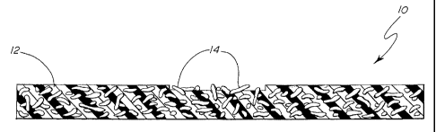
Figure 1 is a cross sectional view of the present invention showing the
etching of
the surface thereof to expose the electrically conductive fiber network
underneath.
Reference will now be made in detail to the present preferred embodiment of
the
invention, an example of which is illustrated in the accompanying drawing.
DETAILED DESCRIPTION OF THE INVENTION
Reference is now made to Figure 1 illustrating an EMI shielding apparatus 10
which is molded or otherwise constructed from an electrically conductive fiber
filled
to polymer composite material into substantially any desired shape. The
apparatus 10 shown
for purposes of illustration is a plate-like cover such as may be utilized to
shield an
electronic component or other article from electromagnetic radiation including
but not
limited to radio frequency waves.
The electrically conductive fiber filled polymer composite material may
15 incorporate substantially any resin or polymer and substantially any
electrically conductive
fiber/particle suitable for the intended purpose. Polymer materials that may
be utilized
include but are not specifically limited to polycarbonate (PC), acrylonitrile
butadiene
styrene (ABS), blends of PC and ABS (PC/ABS), polyethylene terephthalate
(PET),
polybutylene terephthalate (PBT), polyamide (PA or nylon), polystyrene (PS),
2o polypropylene (PP), polyethylene (PE), polyphenylene sulfide (PPS),
polyphenylene oxide
(PPO), syndiotactic polystyrene (SPS), thermoplastic elastomer (TPE), liquid
crystal
polymer (LCP), polyvinyl chloride (PVC), polyacrylate, polyurethane (PUR) and
acetal
copolymer (POM). Essentially all thermoset resins that may be used to produce
molded
articles (for example epoxy resins, polyester resins and phenolic resins) may
be used in the
25 present invention.
Fiber materials with measurable electrical conductivity that may be utilized
include
but are not limited to carbon, graphite, stainless steel, nickel, copper,
iron, steel, silver,
gold, aluminum and any combination of metals and carbon or glass or plastic
particles or
fibers (for example,metal plated glass beads and/or fibers, metal plated
carbon fibers or
3o particles, metal plated plastic beads or fibers.)
Fiber loading may be anywhere between about 5% to about 40% and more
typically falls in a range between about 10% to about 20%. The composite
material may
be prepared in a number of ways including but not limited to extrusion
compounding with
3
CA 02416911 2003-O1-21
WO 02/19346 PCT/USO1/26046
a polymer and a chopped conductive fiber or particles; pultrusion or wire-
coating polymer
over conductive long-fiber. Output from the above two typical processing
methods is
subsequently pelletized to a nominal length of from 0.125 to 0.375 inches
(3.175 to 9.525
mm). Additionally, chopped conductive fibers may be dry-blended with polymer
pellets
as a master batch.
The resulting polymer composite material is molded into substantially any
desired
shape so as to provide a housing shield or shroud to cover an article and
thereby provide
the desired EMI shielding to the article. While useful for many applications,
"as molded",
electrically conductive fiber filled polymer composites suffer from some
limitations, such
as lower line or point-to-point surface conductivity and poor aesthetics.
Specifically,
when flat surfaces of two "as molded" composite parts are pressed together
with a
relatively large contacting area or interface, the surface conductivity
(ohm/sq) is generally
acceptable for most applications. However, when measured by using a point-to-
point
contact resistance method, such as using two probes with needle points from a
standard
ohm-meter, the readings of surface contact resistance are usually very high
and sometimes
not even measurable. The thin covering layer of polymer on the surface of the
parts, or
sometimes the presence of resin rich areas/spots on the surface of the molded
parts are the
main cause for this phenomenon.
Unfortunately, the high line or point-to-point surface contact resistance of
as
2o molded composite parts prevents their use for many EMI shielding
applications. For
example, many applications in the electronic industry require low line or
point-to-point
contact resistance in order to form a complete electrically conductive path
necessary to be
EMI shielding effective.
In accordance with the present invention, it is possible to significantly
improve the
line or point-to-point surface contact resistance of the electrically
conductive fiber filled
polymer composite 10. This is done by evaporating a thin polymer layer from
the surface
of the composite 10 thereby exposing the electrically conductive fiber network
underneath.
Specifically, the surface 12 of the apparatus 10 is etched to a depth of
between about 1 to
about 250 microns (about 0.001 mm to about 0.250 mm) and more typically to
between
3o about 1 to about 50 microns (about 0.001 mm to about 0.050 mm). The exposed
electrically conductive fiber network 14 that results significantly reduces
the line or point-
to-point surface contact resistance of the apparatus by perhaps a factor of 10
- 100. In
some cases the effect will change a non conductive surface to one with
measurable
4
CA 02416911 2003-O1-21
WO 02/19346 PCT/USO1/26046
conductivity. As a consequence, the apparatus 10 is characterized by the
necessary line or
point-to-point surface contact resistance to allow its use for many additional
applications
for which as molded composites are not generally suited.
The evaporating or etching may be performed by using a laser. Many different
types of lasers may be used for this purpose including but not necessarily
limited to dot
matrix, focused-spot and stencil (mask) systems. Lasers useful for the
intended purpose
include but are not limited to (1) stroke Nd: YAG, (neodymium doped yttrium
aluminum
garnet) CW (continuous wave) diode-pumped (2) Nd:YAG, CW lamp-pumped, (3)
frequency-doubled ND:YAG, (4) helium-neon, (5) stroke CO2, sealed RF excited,
(6)
1o mask CO2, pulsed TEA and (7) mask Excimer, pulsed.
The laser is operated at a power level of between about 3 to about 150 watts
and
more typically between about 10 to about 50 watts. The laser may be moved
across the
surface of the composite or apparatus 10 at a laser head speed of between
about 1 to about
500 inches/second (about 0.09 to about 45.72 kilometers/hour)and more
typically about 10
to about 100 inches/second (about 0.91 to about 9.14 kilometers/hour). This
allows the
etching of a pattern across the surface of the apparatus 10. Such a pattern
may be matched
with the etched pattern on an adjacent apparatus 10 in order to provide
desired line or
point-to-point surface contact resistance customized for a particular
application.
Of course, it should be appreciated that the etching also functions to reduce
the
2o variability of the surface contact resistance of the apparatus. If desired,
the power level of
the laser as well as the direction and speed of movement of the laser head may
also be
controlled by computer program. This allows the automated, high speed etching
of even
complicated patterns and the production of parts or apparatus 10 with
generally consistent
overall properties and line or point-to-point contact resistance. Further,
laser etching is
relatively low in cost using only electrical power. In addition, the laser
etching changes
the surface texture of the molded parts advantageously enhancing the adhesion
of two
different parts or materials wherever a joint is necessary.
The following examples are presented to further illustrate the invention, but
it is
not to be considered as being limited thereto.
Example 1
Seven inch diameter round plaques of electrically conducting fiber filled
polymer
composite material lmm thick were etched or engraved using a Xenetch laser
engraving
CA 02416911 2003-O1-21
WO 02/19346 PCT/USO1/26046
system. The laser was generated by using a COz tube with a laser beam width of
0.003
inch (0.0762 mm) and an x-y table dimension of 18 inches x 30 inches (45.72 cm
x 76.2
cm). The maximum power level was 25 watts. The maximum laser head speed was
100
inch/second (9.14 kilometers/hour). The engraving pattern was 1 cm x 1 cm
squares in
spacing of 1 cm to produce 3 or 4 squares per sample. The cutting depth varied
depending
upon the power level, laser head speed and density of the composite material.
The type of
polymer, type of fiber and fiber load rate for various plaques etched in this
example and
the results of the laser etching are presented in Table 1 below.
TABLE 1
SampleFiber Resin ThicknessPower Speed Surface Surface
mm watt inch/secConductivityaConductivityb
km/hr
1 15%NiCFNylon663.2 25 50 3 0.3
4.57
2 15%NiCFPCABS 3.2 25 50 4 to 8 1 to 2
4.57
3 15%NiCFPCABS 3.2 25 50 6 to 30 0.8 to 1.5
4.57
4 15%NiCFPCABS 3.2 25 50 4 to 8 1
4.57
5 15%NiCFTPE 3.2 25 50 50 to 30k 15 to 20
4.57
a 50 psi (344 kPa) before laser etching, ohm/sqr
b 50 psi (344 kPa) after laser etching, ohm/sqr
Example 2
In this experiment, plaques 7 inches (17.78 cm) in diameter and various
thickness
were selected for Nickel coated carbon fiber filled polymer composite. A
qurdrant surface
of each plaque was etched by using the same COZ laser as example #1 for each
given
processing conditions. The surface conductivity in ohms per square was
measured under
the pressure of 1 psi (6.89 kPa). The results are summarized in Table 2.
6
CA 02416911 2003-O1-21
WO 02/19346 PCT/USO1/26046
TABLE 2
SampleFiber Resin ThicknessPowerSpeed Surface Surface
mm watt inch/secConductivityConductivity
km/hr
1 10%NiCFPCABS 2 25 45 >20M 3.2
4.11
2 15%NiCFPCABS 1 25 45 75 2.5
4.11
3 15%NiCFPBT 1 25 45 >20M 4.5
4.11
4 15%NiCFNylon61 25 45 lOk 4.7
4.11
20%NiCFPCABS 1 25 45 42 1.7
4.11
a 1 psi (6.89 kPa) before laser etching, ohmlsqr
b 1 psi (6.89 kPa) after laser etching, ohm/sqr
5
Example 3
In this experiment, plaques 7 inches (17.78 cm) in diameter and 1 mm thick
were
selected for each electrically conducting fiber filled polymer composite.
Three squares of
1 cm x 1 cm were etched into the surface of each plaque using a COz laser for
each given
to set of processing conditions. The results axe summarized in Table 3 below.
TABLE 3
SampleFiber Resin ThiclrnessPowerSpeed 2 Points 2 Points
Contact Contact
nun watt inch/secResistanceaResistanceb
km/hr
1 10%NiCFPCABS 1 25 30 >10k 35
2.74
2 10%NiCFPCABS 1 15 30 >10k 37
2.74
3 10%NiCFPCABS 1 25 60 >10k 33
5.49
4 15%NiCFPCABS 1 25 30 >1k 7
2.74
5 15%NiCFPCABS 1 15 30 >1k 14
2.74
6 15%NiCFPCABS 1 25 60 >1k 8
5.49
a before laser etching, ohms
b after laser etching, ohms
The foregoing description of a preferred embodiment of the invention has been
presented for the purposes of illustration and description. It is not intended
to be
exhaustive or to limit the invention to the precise form disclosed. Obvious
modifications
or variations are possible in light of the above teachings. The embodiment was
chosen and
7
CA 02416911 2003-O1-21
WO 02/19346 PCT/USO1/26046
described to provide the best illustration of the principles of the invention
and its practical
applications to thereby enable one of ordinary skill in the art to utilize the
invention in
various embodiments and with various modifications as are suited to the
particular use
contemplated. All such modifications and variations are within the scope of
the invention
as determined by the appended claims when interpreted in accordance with the
breadth to
which they are fairly, legally and equitably entitled.
8