Note: Descriptions are shown in the official language in which they were submitted.
CA 02417298 2003-O1-22
1
D E S C R I P T I 0 N
OPTICAL MODULATION DEVICE HAVING EXCELLENT
ELECTRIC CHARACTERISTICS FOR EFFECTIVELY
RESTRICTING THERMAL DRIFT AND METHOD FOR
MANUFACTURING THE SAME
Technical Field
The present invention relates to an optical
modulation device and a method for manufacturing the
same, and particularly to an optical modulation device
for modulating an incident light using an electro-optic
effect, and a method for manufacturing the same.
Background Art
It is well known that materials such as lithium
niobate (LiNb03) have an electro-optic effect by which
a refractive index of a light is changed by applying
an electric field.
A lithium niobate optical modulation device of
a traveling wave electrode type (LN optical modulation
device) configured by forming an optical waveguide and
a traveling-wave electrode on a substrate made of such
a material (hereinafter, abbreviated as an LN
substrate) is used in high volume optical transmission
systems of 2.5 Gbit/s and 10 Gbit/s because of its good
chirping characteristics.
In recent years, as this LN optical modulation
device is to be further applied to an optical
transmission system having a very high capacity of
CA 02417298 2003-O1-22
2
40 Gbit/s, the device needs to be further developed in
light of its importance in the field of optical
communications .
FIG. 18 is a perspective view showing a schematic
configuration of a typical optical modulation device
using lithium niobate (LiNb03).
Further, FIG. 19 is a sectional view of the
optical modulation device in FIG. l8 taken along the
line 19-19.
In FIG. 18 and FIG. 19, an optical waveguide 2 is
formed from one end of an LN substrate 1 to the other
end thereof in contact with an upper surface of the LN
substrate 1 in the z-cut state where the lithium
niobate (LiNb03) is cut in the z-surface direction of
a crystal surface.
The optical waveguide 2 is branched into two
optical waveguides 2a and 2b at the midpoint of the LN
substrate 1, which are brought together again in the
vicinity of the other end.
A buffer layer 5 commonly covering the upper
surfaces of these optical waveguides 2a and 2b and the
upper surface of the LN substrate 1 is formed.
A center electrode 3 is formed at a position
opposite to the one optical waveguide 2a in the upper
surface of the buffer layer 5.
Further, in the upper surface of the buffer
layer 5, ground electrodes 4a and 4b are formed,
CA 02417298 2003-O1-22
3
respectively, at the position not opposite to the one
optical waveguide 2a and at the position opposite to
the other optical waveguide 2b so as to sandwich the
center electrode 3.
The discussion here can be applied to any
traveling-wave electrode in any form, but as one
example, it is assumed that a coplanar waveguide (CPW)
having one center electrode 3 and two ground electrodes
4a, 4b is employed.
Furthermore, the optical waveguides 2, 2a, 2b are
so-called thermal diffusion optical waveguides formed
by, after depositing a metal titanium (Ti) in the
thickness from several tens nm to 100 nm or more,
patterning it in the width in the order of 6 to 8 ~,m,
and further thermally diffusing it at a temperature of
about 1000°C .
In the optical modulation device shown in FIG. 18
and FIG. 19, the optical waveguides 2, 2a, and 2b as
a Mach-Zehnder interferometer are configured.
In addition, a one-linear optical waveguide may be
employed instead of the Mach-Zehnder interferometer in
the case of a phase modulation device.
The buffer layer 5 is deposited between the
traveling-wave electrode formed of the center electrode
3 and the ground electrodes 4a, 4b and the LN substrate
1 in order to restrict an absorption loss which a light
guided through the optical waveguides 2a and 2b
CA 02417298 2003-O1-22
4
receives from the metal (Au is generally employed)
which is the traveling-wave electrode (center
electrode 3, ground electrodes 4a, 4b).
The buffer layer 5 is generally made of Si02 which
is as thick as about l dun.
The buffer layer 5 is used for reducing a
microwave equivalent refractive index of an electric
signal guided through the traveling-wave electrode
formed of the center electrode 3 and the ground
electrodes 4a, 4b (or microwave equivalent refractive
index of the traveling-wave electrode) to be made
closer to an equivalent refractive index of the light
guided through the optical waveguides 2a and 2b (or
equivalent refractive index of the optical waveguide),
and making a characteristic impedance closer to 5052, as
well as for restricting the absorption loss.
FIG. 20 is a diagram shown for explaining
operations of the optical modulation device having such
a structure.
In other words, FIG. 20 shows a desirable
distribution of an electric line of force 7a in the
case where a voltage is applied between the center
electrode 3 and the ground electrodes 4a, 4b of the
traveling-wave electrode.
As can be understood from FIG. 20, since the
orientation of the electric line of force 7a across
the two optical waveguides 2a and 2b is reverse to
CA 02417298 2003-O1-22
the orientation of both the optical waveguides, a phase
of the light guided through the two optical waveguides
2a and 2b is shifted by 180° (~) in the optical
waveguide of the Mach-Zehnder interferometer so that
5 the OFF state of the light can be realized.
However, even an optical modulation device having
a sectional structure shown in FIG. 19 still has
disadvantages, as described below.
Since the LN substrate 1 has a pyroelectric
effect, as shown in FIG. 21, when the temperature of
the LN substrate 1 is changed, a charge 9a is induced
on the surface thereof.
However, since the buffer layer 5 made of Si02
does not have conductivity, in the center electrode 3
and the ground electrodes 4a, 4b of the traveling-wave
electrode, a charge 9b having a polarity opposite to
the polarity of the charge 9a induced on the surface of
the LN substrate 1 is induced on the surface opposite
the LN substrate 1 through an external circuit.
As a result, an electric line of force 7b is
generated between the charge 9a induced on the LN
substrate 1 and the charge 9b induced on the center
electrode 3 and the ground electrodes 4a, 4b of the
traveling-wave electrode.
However, as can be understood from FIG. 21, since
this electric line of force 7b is generated at random,
the electric line of force 7a generated by the voltage
CA 02417298 2003-O1-22
6
applied between the center electrode 3 and the ground
electrodes 4a, 4b for operating the optical modulation
device is eliminated at random.
Therefore, the optical modulation efficiency of
the optical modulation device widely varies, due to
changes in temperature.
The change of this optical modulation efficiency
occurs as a phenomenon of an operating point shift.
This operating point shift due to the temperature
is called thermal drift.
In order to solve the disadvantages of the
aforementioned optical modulation device, there has
been proposed an optical modulation device having
a sectional shape shown in FIG. 22 (refer to Jpn. Pat.
Appln. KOKOKU Publication No. 4-22485).
In addition, in FIG. 22, the diagram is shown in
a somewhat enlarged manner in the vertical direction in
order to explain the operations.
Further, in the optical modulation device shown in
FIG. 22, like reference numerals are denoted to like
parts identical to those in the optical modulation
device shown in FIG. 19.
Furthermore, a perspective view showing the entire
structure of the optical modulation device shown in
FIG. 22 is substantially identical to the perspective
view of the optical modulation device shown in FIG. 18.
In the optical modulation device shown in FIG. 22,
CA 02417298 2003-O1-22
7
a conductive film 6 is formed on the upper side of the
buffer layer 5, and the center electrode 3 and the
ground electrodes 4a, 4b are formed on the upper side
of the conductive film 6.
In other words, as shown in FIG. 22, a charge 9c
having a polarity opposite the polarity of the charge
9a induced on the LN substrate 1 due to the
pyroelectric effect of the LN substrate 1 is induced on
the conductive film 6 in contact with the center
electrode 3 and the ground electrodes 4a, 4b.
As a result, an electric line of force 7c between
the Charge 9a induced on the LN substrate 1 and the
charge 9c induced on the conductive film 6 becomes
uniform as shown in FIG. 22 so that a random electric
line of force is not across the optical waveguides 2a
and 2b .
This is to say, the changes of the refractive
index caused by the charge 9a induced by the
pyroelectric effect become the same in the two optical
waveguides 2a and 2b.
Thereby, in the optical modulation device shown in
FIG. 22, the phase difference of the lights being
guided through the two optical waveguides 2a and 2b is
caused by only the voltage externally applied, which
enables this device to function as an optical
modulation device.
In addition, an Si film having the thickness of
CA 02417298 2003-O1-22
about 100 nm is employed as the conductive film 6.
However, even an optical modulation device
employing the conductive film 6 in this manner still
has important problems to be solved.
That is, as is well known, the control of the
electric conductivity of the conductive film 6 is very
difficult, which means that the conductivity thereof
easily varies, in the order of 2 to 3 decimal places,
due to impurities in the film.
When the conductivity of the conductive film 6 is
too low, the device closely resembles an optical
modulation device which does not employ a conductive
film 6 shown in FIG. 19, meaning that the problems
which this optical modulation device has occurs.
On the contrary, when the conductivity of the
conductive film 6 is too high, the center electrode 3
and the ground electrodes 4a, 4b enter an electrically
conductive state.
As a result, the characteristic impedance of
the traveling-wave electrode formed of the center
electrode 3 and the ground electrodes 4a, 4b is very
lowered, thus the electric characteristics and high
frequency characteristics are deteriorated, or a large
current flows between the center electrode 3 and the
ground electrodes 4a, 4b, so that the device itself is
destroyed.
In this manner, it is remarkably difficult to form
CA 02417298 2003-O1-22
9
a conductive film 6 having an appropriate conductivity
with excellent reproducibility, and the optical
modulation device employing the conductive film 6 shown
in FIG. 22 has a large problem in the reproducibility
in the manufacture thereof.
In order to solve the disadvantages of the
aforementioned optical modulation device, there has
been further proposed an optical modulation device
having a sectional shape shown in FIG. 23 (Japanese
Patent No. 2873203).
In the optical modulation device shown in FIG. 23,
like reference numerals are denoted to like parts
identical to those in the optical modulation device
shown in FIG. 19.
In the optical modulation device shown in FIG. 23,
the width of the conductive film 6a is set to be finite
so that the conductive film 6a is made to contact only
the center electrode 3.
Further, in the optical modulation device shown in
FIG. 23, a configuration is employed in which a gap 10,
having a width G, is provided between the ground
electrodes 4a, 4b at both sides, and a conductive film
6a, so that the ground electrodes 4a, 4b and the
conductive film 6a do not contact.
Next, operations of the optical modulation device
in which the width of the conductive film 6a is
restricted in this manner are described.
CA 02417298 2003-O1-22
With respect to the electric field applied to the
optical waveguide 2a positioned below the center
electrode 3, an electric line of force 7d caused by the
uniform electric field distribution can be obtained by
5 the same principles as the optical modulation device
shown in FIG. 22 other than the influence of the
electric field from the charge 9a induced by the
pyroelectric effect in an area A and an area B in
FIG. 23 due to the presence of the conductive film 6a.
10 On the other hand, with respect to the ground
electrodes 4a and 4b, the ground electrodes 4a and 4b
are not in contact with the conductive film 6a
different from the optical modulation device shown in
FIG. 22.
Therefore, with respect to the optical waveguide
2b positioned in the area B in FIG. 23, it is predicted
that the problem similar to that of the optical
modulation device shown in FIG. 19 occurs.
In order to avoid that, the following devisal is
made.
The thickness of the traveling waveguide of the
center electrode 3 and the ground electrodes 4a, 4b is
set to be as thick as several Nxn or more.
In other words, since the traveling-wave electrode
made of metal (Au is generally used as a material, but
various other meals such as aluminum, copper, and the
like can be employed) and the LN substrate 1 of
CA 02417298 2003-O1-22
11
dielectrics have different thermal expansion
coefficients, a temperature-dependent stress is
generated in the LN substrate 1.
The internal stress due to plating becomes larger
to the extent where a bow occurs in the LN substrate 1
when plating is performed to several ~.m or more.
The internal electric field occurs due to the
photoelastic effect caused by this internal stress.
On the other hand, as described in the optical
modulation device shown in FIG. 19, the charge 9a
occurs in the surface of the LN substrate 1 by the
pyroelectric effect when the temperature is changed
such that the internal electric field occurs.
In the optical modulation device shown in FIG. 23,
the gap 10 having the width G is provided between
the conductive film 6a and the ground electrodes 4a, 4b
at both sides and the width G is defined by
photolithography. Therefore, the internal electric
field by the photoelastic effect caused by the internal
stress and the internal electric field by the
pyroelectric effect caused by the temperature change
are eliminated.
Accordingly, in the state where the characteristic
impedance of the traveling-wave electrode formed of the
center electrode 3 and the ground electrodes 4a, 4b is
maintained in a constant state, it is prevented that
the electric line of force 7a due to the voltage
CA 02417298 2003-O1-22
12
applied between the center electrode 3 and the ground
electrodes 4a, 4b for operating the optical modulation
device is eliminated at random.
However, even an optical modulation device in
which the width of the conductive film 6a is restricted
shown in FIG. 23 has the following further problem to
be solved.
In other words, as can be easily assumed from the
above description, it is not easy to appropriately
eliminate the two internal electric fields described
above generated in the LN substrate 1.
Further, when it cannot be realized, a random
electric field is applied in the optical waveguide 2b
positioned below the ground electrode 4b as with the
optical modulation device shown in FIG. 19.
Particularly, the influence of the random electric
field from the area A is large.
In addition, the random electric field from the
area B particularly acts on the optical waveguide 2a
below the center electrode 3.
As a result, the operating point in the optical
modulation of the optical modulation device is largely
deviates according to the temperature.
The traveling-wave electrode formed of the center
electrode 3 and the ground electrodes 4a, 4b is
generally formed by electrolytic plating method, but
since a temperature variation or a current variation is
CA 02417298 2003-O1-22
13
present in the electrolytic plating solution, even when
the same current is flowed at the same solution
temperature at the time of plating, a slight variation
occurs in the particle of the grown plating or the
thickness of the electrode every run-to-run of the
plating step.
Therefore, the internal stress caused by the
formed plating is different in every plating.
Furthermore, in the electrolytic plating solution,
a slight variation is present in the particles of the
plating or the thickness of the electrode even in the
same wafer, because of the fact that a variation is
present in the current or the solution temperature
between the plating electrode and the wafer, and the
convection of the electrolytic plating solution, so
that the internal stress is different in every chip.
As a result, it is difficult to determine the
appropriate width G of the gap 10 for eliminating the
internal electric field caused by the photoelastic
effect due to the thermal stress and the internal
electric field caused by the pyroelectric effect due to
the temperature change.
Additionally, since the gap 10 is realized by
photolithography, it is required to be performed before
plating the traveling-wave electrode to 10 dun or more.
That is, the gap 10 is required to be formed at
the stage where each modulation device including the LN
CA 02417298 2003-O1-22
14
substrate 1 is cut out from the wafer, namely in the
wafer stage.
As a result, it has to be performed before
measuring the thermal drift characteristics of each
modulation device, and the determination of the width G
of the gap 10 is difficult and is not necessarily
appropriately performed with respect to each chip so
that a yield of the optical modulation device including
the LN substrate 1 is restricted.
Moreover, as described above, the effect obtained
by eliminating the two electric fields described above
generated in the LN substrate 1 is limited, and
therefore the thickness of the plating of the
traveling-wave electrode is limited to about 10 to
2 0 ~.m .
However, in the actual optical modulation device,
in order to achieve a velocity matching between a
microwave and a light required for broadbandizing of
the optical modulation, sometimes the traveling-wave
having the thickness of 25 ~.un to 30 ~m or more may be
required.
In this case, the optical modulation device having
a mechanism for eliminating the two internal electric
fields shown in FIG. 23 cannot be used and application
has limitation.
Disclosure of Invention
The present invention is made in view of the above
CA 02417298 2003-O1-22
circumstances, and it is an object of the present
invention to provide a small-sized and high-speed
optical modulation device in which a conductive film is
employed and a center electrode and a ground electrode
5 are electrically separated, so that an electrical
resistance between the center electrode and the ground
electrode is made larger, device destruction is
avoided, and excellent high frequency characteristics
are attained, facilitation of structure determination
10 or manufacturing process or reproducibility of
manufacture is secure, and further, thermal drift is
effectively restricted also for a traveling-wave
electrode (center electrode and ground electrode)
having the thickness of 20 ~m or more generally
15 required, and as a result, an operating point shift
caused by thermal drift is small.
It is another object of the present invention to
provide a method for manufacturing a small-sized and
high-speed optical modulation device in which a
conductive film is employed and a center electrode and
a ground electrode are electrically separated so that
an electrical resistance between the center electrode
and the ground electrode is made larger, device
destruction is avoided and excellent high frequency
characteristics are attained, facilitation of structure
determination or manufacturing process or
reproducibility of manufacture is secure, and further,
CA 02417298 2003-O1-22
16
thermal drift is effectively restricted also for a
traveling-wave electrode (center electrode and ground
electrode) having the thickness of 20 ~,un or more
generally required, and as a result, an operating point
shift caused by thermal drift is small.
In order to achieve the above object, according to
a first aspect of the present invention, there is
provided an optical modulation device comprising:
a substrate (1) having an electro-optic effect;
an optical waveguide (2) which is formed on the
substrate and guides an incident light;
a first buffer layer (5) which covers an upper
surface of the substrate;
a conductive film (6) formed above the first
buffer layer;
a center electrode (3) and a ground electrode (4)
to apply a voltage in order to induce an electric field
on the optical waveguide; and
a second buffer layer (8) formed between the
conductive film and at least one of the center
electrode and the ground electrode,
wherein the conductive film is formed to be
present on at least a part below the ground electrode,
and
a light guided through the optical waveguide is
modulated by changing a phase by a voltage applied to
the optical waveguide.
CA 02417298 2003-O1-22
1T
In order to achieve the above object, according to
a second aspect of the present invention, there is
provided an optical modulation device according to the
first aspect, wherein the center electrode is in
contact with the conductive film and the ground
electrode is not in contact with the conductive film.
In order to achieve the above object, according to
a third aspect of the present invention, there is
provided an optical modulation device according to the
first or second aspect, wherein a second buffer layer
is formed between the ground electrode and the
conductive film.
In order to achieve the above object, according to
a fourth aspect of the present invention, there is
provided an optical modulation device according to the
first aspect, wherein the ground electrode is in
contact with the conductive film and the center
electrode is not in contact with the conductive film.
In order to achieve the above object, according to
a fifth aspect of the present invention, there is
provided an optical modulation device according to the
first or fourth aspect, wherein a second buffer layer
is formed between the center electrode and the
conductive film.
In order to achieve the above object, according to
a sixth aspect of the present invention, there is
provided an optical modulation device according to the
CA 02417298 2003-O1-22
18
first aspect, wherein the center electrode includes a
plurality of center electrode members, at least one of
the plurality of center electrode members is in contact
with the conductive film, and the ground electrode is
not in contact with the conductive film.
In order to achieve the above object, according to
a seventh aspect of the present invention, there is
provided an optical modulation device according to the
first aspect, wherein the center electrode includes a
plurality of center, electrode members, all the
plurality of center electrode members are in contact
with the conductive film, and the ground electrode is
not in contact with the conductive film.
In order to achieve the above object, according to
an eighth aspect of the present invention, there is
provided an optical modulation device according to the
sixth or seventh aspect, wherein a second buffer layer
is formed between the ground electrode and the
conductive film.
In order to achieve the above object, according to
a ninth aspect of the present invention, there is
provided an optical modulation device according to the
first aspect, wherein the ground electrode includes a
plurality of ground electrode members, at least one of
the plurality of ground electrode members is in contact
with the conductive film, and the center electrode is
not in contact with the conductive film.
CA 02417298 2003-O1-22
19
In order to achieve the above object, according to
a tenth aspect of the present invention, there is
provided an optical modulation device according to the
ninth aspect, wherein a second buffer layer is formed
between the center electrode and the conductive film.
In order to achieve the above object, according to
an eleventh aspect of the present invention, there is
provided an optical modulation device according to the
first aspect, wherein a second buffer layer is formed
between the center electrode, the ground electrode and
the conductive film, the center electrode and the
ground electrode are not in contact with the conductive
film, and part of the conductive film is electrically
connected with the outside.
In order to achieve the above object, according to
a twelfth aspect of the present invention, there is
provided an optical modulation device according to the
eleventh aspect, wherein the center electrode includes
a plurality of center electrode members.
In order to achieve the above object, according to
a thirteenth aspect of the present invention, there is
provided an optical modulation device according to the
eleventh aspect, wherein the ground electrode includes
a plurality of ground electrode members.
In order to achieve the above object, according to
a fourteenth aspect of the present invention, there is
provided n optical modulation device according to the
CA 02417298 2003-O1-22
first aspect, wherein the center electrode includes a
plurality of center electrode members and the ground
electrode includes a plurality of ground electrode
members, at least one of the plurality of center
5 electrode members is in contact with the conductive
film, at least one of the plurality of ground electrode
members is in contact with the conductive film, and the
at least one of the plurality of center electrodes or
the at least one of the plurality of ground electrodes
10 is not in contact with the conductive film.
In order to achieve the above object, according to
a fifteenth aspect of the present invention, there is
provided an optical modulation device according to the
ninth or tenth aspect, wherein only part of the ground
15 electrode is in contact with the conductive film.
In order to achieve the above object, according to
a sixteenth aspect of the present invention, there is
provided a method for manufacturing an optical
modulation device, comprising:
20 providing a substrate (1) having an electro-optic
effect;
forming an optical waveguide (2) which guides an
incident light on the substrate;
forming a first buffer layer (5) which covers an
upper surface of the substrate;
forming a conductive film (6) above the first
buffer layer;
CA 02417298 2003-O1-22
21
forming a center electrode (3) and a ground
electrode (4) which apply a voltage in order to induce
an electric field on the optical waveguide; and
forming a second buffer layer (8) between the
conductive film and at least one of the center
electrode and the ground electrode,
wherein the conductive film is formed to be
present on at least a part below the ground electrode,
and
a light guided through the optical waveguide is
modulated by changing a phase by a voltage applied to
the optical waveguide.
In the optical modulation device configured in
this manner, a charge having the polarity opposite to
the polarity of a charge to be induced on a surface of
the substrate having an electro-optic effect by a
pyroelectric effect is induced on the conductive film
via a traveling-wave electrode formed of the canter
electrode and the ground electrodes from an external
circuit when a temperature is changed.
As a result, in the optical modulation device, an
electric field by induced mutual charges becomes
uniform in an area where the optical waveguide is
present so that an operating point shift due to the
thermal drift is finally restricted without influencing
the optical modulation.
Further, in the optical modulation device, since
CA 02417298 2003-O1-22
22
the center electrode and the ground electrode
configuring the traveling-wave electrode are
electrically separated, even when the conductivity of
the conductive film for restricting the thermal drift
due to the pyroelectric effect becomes larger,
excellent electric characteristics, including high
frequency characteristics can be attained.
Brief Description of Drawings
FIG. 1 is a schematic sectional view showing
a schematic configuration of an optical modulation
device according to a first embodiment;
FIG. 2 is a schematic sectional view showing
a schematic configuration of an optical modulation
device according to a second embodiment;
FIG. 3 is a schematic sectional view showing
a schematic configuration of an optical modulation
device according to a third embodiment;
FIG. 4 is a schematic sectional view showing
a schematic configuration of an optical modulation
device according to a fourth embodiment;
FIG. 5 is a schematic sectional view showing
a schematic configuration of an optical modulation
device according to a fifth embodiment;
FIG. 6 is a schematic sectional view showing
a schematic configuration of an optical modulation
device according to a sixth embodiment;
FIG. 7 is a schematic sectional view showing
CA 02417298 2003-O1-22
23
a schematic configuration of an optical modulation
device according to a seventh embodiment;
FIG. 8 is a schematic sectional view showing
a schematic configuration of an optical modulation
device according to a eighth embodiment;
FIG. 9 is a schematic sectional view showing
a schematic configuration of an optical modulation
device according to a ninth embodiment;
FIG. 10 is a schematic sectional view showing
a schematic configuration of an optical modulation
device according to a tenth embodiment;
FIG. 11 is a schematic sectional view showing
a schematic configuration of an optical modulation
device according to a eleventh embodiment;
FIG. 12 is a schematic sectional view showing
a schematic configuration of an optical modulation
device according to a twelfth embodiment;
FIG. 13 is a schematic sectional view showing
a schematic configuration of an optical modulation
device according to a thirteenth embodiment;
FIG. 14 is a schematic sectional view showing
a schematic configuration of an optical modulation
device according to a fourteenth embodiment;
FIG. 15 is a schematic sectional view showing
a schematic configuration of an optical modulation
device according to a fifteenth embodiment;
FIG. 16 is a schematic sectional view showing
CA 02417298 2003-O1-22
24
a schematic configuration of an optical modulation
device according to a sixteenth embodiment;
FIG. 17 is a schematic sectional view showing
a schematic configuration of an optical modulation
device according to a seventeenth embodiment;
FIG. 18 is a perspective view showing a schematic
configuration of a conventional typical optical
modulation device;
FIG. 19 is a schematic sectional view showing
a schematic configuration of a conventional optical
modulation device;
FIG. 20 is a diagram for explaining operations of
the conventional optical modulation device;
FIG. 21 is a diagram for explaining a problem of
the conventional optical modulation device;
FIG. 22 is a schematic sectional view showing
a schematic configuration of another conventional
optical modulation device; and
FIG. 23 is a schematic sectional view showing
a schematic configuration of still another conventional
optical modulation device.
Best Mode for Carrying Out the Invention
Hereinafter, respective embodiments according to
the present invention will be described with reference
to the drawings.
(First embodiment)
FIG. 1 is a schematic sectional view showing
CA 02417298 2003-O1-22
a schematic configuration of an optical modulation
device according to a first embodiment of the present
invention.
The optical modulation device shown in FIG. 1 is
5 somewhat enlarged in the vertical direction in order to
simplify the description.
Further, in the optical modulation device shown in
FIG. 1, like reference numerals are denoted to like
parts identical to those in the conventional optical
10 modulation device shown in FIG. 22, and detailed
description of the overlapping parts will be omitted.
A perspective view showing the entire structure of
the optical modulation device shown in FIG. 1 is
substantially the same as the perspective view of the
15 conventional optical modulation device shown in
FIG. 18.
In other words, in the optical modulation device
according to the first embodiment of the present
invention, as shown in FIG. l, an optical waveguide 2
20 is formed from one end of a LN substrate 1 to the other
end in contact with the upper surface in the LN
substrate 1 in the Z-cut state.
The optical waveguide 2 is branched into two
optical waveguides 2a and 2b at the midpoint of the LN
25 substrate 1, which are brought together again in the
vicinity of the other end.
A buffer layer 5 is formed so as to cover
CA 02417298 2003-O1-22
26
the upper surfaces of these optical waveguides 2a, 2b
and the upper surface of the LN substrate 1.
A conductive film 6 is formed at the upper surface
of the buffer layer S.
Further, a center electrode 3 is formed at the
position opposite to the one optical waveguide 2a in
the upper surface of the conductive film 6.
Furthermore, second insulating buffer layers 8a
and 8b are formed, respectively, at the position not
opposite to the one optical waveguide 2a and at the
position opposite to the other optical waveguide 2b so
as to sandwich the center electrode 3.
Ground electrodes 4a and 4b are formed on the
second buffer layers 8a and 8b, respectively.
Specifically, in the optical modulation device
according to this first embodiment, the center
electrode 3 and the conductive film 6 are in contact as
with the conventional optical modulation device shown
in FIG. 22.
The ground electrodes 4a and 4b are not in contact
with the conductive film 6 different from the
conventional optical modulation device shown in
FIG. 22.
Further, in the optical modulation device
according to this first embodiment, since the
conductive film 6 is entirely formed across the
substrate surface direction, a gap 10 is not present
CA 02417298 2003-O1-22
27
and the conductive film 6 is present below the ground
electrodes 4a and 4b different form the conventional
optical modulation device shown in FIG. 23.
Next, a procedure of manufacturing the optical
modulation device according to the first embodiment
will be described.
In the optical modulation device according to the
first embodiment, the Ti thermal diffusion optical
waveguides 2a and 2b are formed on the Z-cut LN
substrate 1 as with the conventional optical modulation
device shown in FIG. 22.
Next, the buffer layer 5 made of Si02 having the
thickness in the order of several tens nm to 1 dun is
deposited on the LN substrate 1 by sputtering or the
like.
Thereafter, the Si film having the thickness of
about 100 nm is formed as the conductive film 6 on the
buffer layer 5.
Then, in order to electrically separate each
ground electrode 4a, 4b and the conductive film 6,
insulation layers for forming the second buffer layers
made of Si02 film having a thickness on the order of
several tens nm to 1 ~,~m are deposited on the conductive
film 6.
Subsequently, the Si02 film other than the
portions under the ground electrodes 4a and 4b to be
formed later is removed by dry etching, wet etching, or
CA 02417298 2003-O1-22
28
the like.
Thereby, the second buffer layers 8a and 8b are
formed, respectively, at the portions under the ground
electrodes 4a and 4b.
At this time, an area where the buffer layer is
not partially present is present, where the conductive
film 6 is exposed on the surface.
Further, after Ti and Au are deposited on the
entire surface, a photo resist is formed for plating-
growing the center electrode 3 and the ground
electrodes 4a, 4b.
Next, after Au having the thickness of about 3 ~.m
to 40 ~,m is grown by the electrolytic plating method
according to a desired optical modulation band, the
photo resist is removed by acetone or the like.
Thereafter, unnecessary Ti and Au are removed by
dry etching or wet etching.
Then, operations of the optical modulation device
according to the first embodiment will be described.
When the temperature of the LN substrate 1 rises,
a charge 9a is induced on the surface of the LN
substrate 1 by the pyroelectric effect.
In the first embodiment, since the center
electrode 3 and the conductive film 6 are in contact, a
charge 9c having the polarity opposite to the polarity
of the charge 9a induced on the surface of the LN
substrate 1 is induced on the conductive film 6 through
CA 02417298 2003-O1-22
29
the center electrode 3 from the external circuit.
The conductive film 6 is present not only under
the center electrode 3 but also under the ground
electrodes 4a and 4b.
Therefore, an electric line of force 7c by the
electric field generated between the charge 9a induced
on the surface of the LN substrate 1 and the charge 9c
induced on the conductive film 6 is uniform in the
areas where the optical waveguides 2a and 2b are
present so that the same refractive index change, that
is, the same phase change is caused for the two optical
waveguides 2a and 2b.
Since the intensity modulation according to the
phase difference between the lights guided through the
two optical waveguides 2a and 2b is generated in the
Mach-Zehnder interferometer, even when the lights
guided through the two optical waveguides 2a and 2b
generate the phase change with the same amount, this
fact does not influence the wave combining.
Further, a charge 9d having the polarity opposite
to that of the charge 9c induced on the conductive film
6 is induced on the ground electrodes 4a and 4b which
are formed on the second insulating buffer layers 8a
and 8b made of Si02 through the external circuit.
However, an electric line of force 7e caused by
both the induced charges 9c and 9d is limited between
the ground electrodes 4a, 4b and the conductive film 6
CA 02417298 2003-O1-22
and is not across the optical waveguides 2a and 2b so
that the optical modulation efficiency is not
influenced.
It is better in manufacture that the second buffer
5 layers 8a and 8b positioned at the lower sides of the
ground electrodes 4a and 4b are extended between the
center electrode 3 and the ground electrodes 4a, 4b at
both sides, which does not cause any problems.
(Second embodiment)
10 FIG. 2 is a schematic sectional view showing
a schematic configuration of an optical modulation
device according to a second embodiment of the present
invention.
In the optical modulation device according to the
15 second embodiment shown in FIG. 2, like reference
numerals are denoted to like parts identical to those
in the optical modulation device according to the first
embodiment shown in FIG. 1, and detailed description of
the overlapping parts will be omitted.
20 In the optical modulation device according to this
second embodiment, the second buffer layers 8a and 8b
positioned at the lower sides of the two ground
electrodes 4a and 4b in the optical modulation device
according to the first embodiment shown in FIG. 1 are
25 extended to the center electrode 3 side.
In this case, it goes without saying that, with
respect to only one ground electrode 4a (4b),
CA 02417298 2003-O1-22
31
the second buffer layer 8a (8b) may be extended to the
center electrode side 3.
In this case, edges of the second buffer layers 8a
and 8b may be etched in order that the edge of at least
one of the second buffer layers 8a and 8b is retreated
in the ground electrode 4a, 4b side.
As described above, according to the optica l
modulation devices of the first and second embodiments,
the thermal drift of the optical modulation by the
pyroelectric effect can be effectively restricted.
Furthermore, according to the optical modulation
devices of the first and second embodiments, the
conductive film 6 is formed not only at the center
electrode 3 but also at the areas of the ground
electrodes 4a and 4b so that the effect of the thermal
drift restriction is remarkable as compared with the
conventional optical modulation device shown in
FIG. 23.
Additionally, in the conventional optical
modulation device shown in FIG. 22, both the center
electrode 3 and the ground electrodes 4a, 4b are in
contact with the conductive film 6 so that the
conductivity of the conductive film 6 largely
influences the electric characteristics as the
traveling-wave electrode and can occasionally cause
device destruction. However, in the optical modulation
devices according to the first and second embodiments,
CA 02417298 2003-O1-22
32
the ground electrodes 4a and 4b are not is contact with
the conductive film 6 and the center electrode 3 and
the ground electrodes 4a, 4b are electrically separated
completely. Accordingly, there is the advantage that
the device destruction does not occur and the
conductivity of the conductive film 6 is not easy to
influence the electric characteristics as the
traveling-wave electrode.
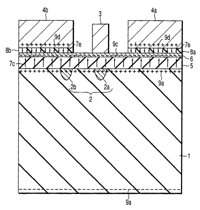
(Third embodiment)
FIG. 3 is a schematic sectional view showing a
schematic configuration of an optical modulation device
according to a third embodiment of the present
invention.
In the optical modulation device according to the
third embodiment shown in FIG. 3, like reference
numerals are denoted to like parts identical to those
in the conventional optical modulation device shown in
FIG. 22, and detailed description of the overlapping
parts will be omitted.
In the optical modulation device according to this
third embodiment, the ground electrodes 4a, 4b and the
conductive film 6 are in contact as with the
conventional optical modulation device shown in
FIG. 22.
However, in the optical modulation device
according to the third embodiment, a second insulating
buffer layer 8c is formed on the center portion of the
CA 02417298 2003-O1-22
33
upper surface of the conductive film 6, and the center
electrode 3 is formed on the second buffer layer 8c.
As a result, in the optical modulation device
according to the third embodiment, the center electrode
3 and the conductive film 6 are not in contact
different from the conventional optical modulation
device shown in FIG. 22.
Now, operations of the optical modulation device
according to the third embodiment will be described
with reference to FIG. 3.
When the temperature of the LN substrate 1 rises,
a charge 9a is induced on the surface of the LN
substrate 1 by the pyroelectric effect.
In the present embodiment, since the ground
electrodes 4a, 4b and the conductive film 6 are in
contact, a charge 9c having a polarity opposite to the
polarity of the charge 9a induced on the surface of the
LN substrate 1 is induced on the conductive film 6
through the ground electrodes 4a and 4b from the
external circuit.
The conductive film 6 is present not only at the
lower sides of the ground electrodes 4a, 4b but also at
the lower side of the center electrode 3.
Therefore, the electric line of force 7c
indicating the electric field generated between the
charge 9a induced on the surface of the LN substrate 1
and the charge 9c induced on the conductive film 6 is
CA 02417298 2003-O1-22
34
uniform in the areas where the optical waveguides 2a
and 2b are present, which causes the same refractive
index changes, that is the same phase changes for the
two optical waveguides 2a and 2b.
Since the intensity modulation according to the
phase difference between the lights guided through the
two optical waveguides 2a and 2b is generated in the
Mach-Zehnder interferometer, even when the lights
guided through the two optical waveguides 2a and 2b
generate the phase changes with same amount, the wave
combining is not influenced.
Further, a charge 9b having a polarity opposite to
the polarity of the charge 9c induced on the conductive
film 6 is induced on the center electrode 3 formed on
the second insulating buffer layer 8c made Si02 through
the external circuit.
An electric line of force 7f due to both the
induced charges 9c and 9b is limited between the center
electrode 3 and the conductive film 6 and is not across
the optical waveguide 2a, which does not influence the
optical modulation efficiency.
In FIG. 3, the width of the buffer layer 8c is set
to be larger than the width of the center electrode 3,
but may be set to be as small as the width of the
center electrode 3 and may be set to be larger to reach
the edge of at least one of the ground electrodes 4a
and 4b or the halfway thereof.
CA 02417298 2003-O1-22
In this manner, also in the optical modulation
device according to this third embodiment, the thermal
drift of the optical modulation by the pyroelectric
effect can be effectively restricted as with the
5 optical modulation devices according to the above first
and second embodiments.
Further, in the optical modulation device
according to the third embodiment, the center electrode
3 and the conductive film 6 are not in contact so that
10 the center electrode 3 and the ground electrodes 4a, 4b
at both sides are electrically separated.
Therefore, it is advantageous that device
destruction does not occur and the conductivity of the
conductive film 6 has a negligible effect on the
15 electric characteristics as the traveling-wave
electrode.
(Fourth embodiment)
FIG. 4 is a schematic sectional view showing a
schematic configuration of an optical modulation device
20 according to a fourth embodiment of the present
invention.
In the optical modulation device according to the
fourth embodiment shown in FIG. 4, like reference
numerals are denoted to like parts identical to those
25 in the optical modulation device according to the third
embodiment shown in FIG. 3, and detailed description of
the overlapping parts will be omitted.
CA 02417298 2003-O1-22
36
In the optical modulation device according to this
fourth embodiment, of the two ground electrodes 4a and
4b of the traveling-wave electrode, part of the lower
surface of the one ground electrode 4b is in contact
with the conductive film 6.
In this case, a second buffer layer 8d is
intervened between the remaining portion of the lower
surface of the one ground electrode 4b and the
conductive film 6.
Further, the second buffer layers 8a, 8c, and 8d
are intervened between the other ground electrode 4a,
the center electrode 3 and the conductive film 6,
respectively.
In the optical modulation device according to the
fourth embodiment configured in this manner, a charge
9c having a polarity opposite to the polarity of the
charge 9a induced on the surface of the LN substrate 1
is induced on the conductive film 6 through the center
electrode 3 and the ground electrodes 4a, 4b from the
external circuit as with the optical modulation devices
according to the above first to third embodiments.
In this manner, also in the present embodiment,
the charge 9c is induced on the conductive film 6 so
that a sufficient effect can be obtained for
restricting the operating point shift caused by the
thermal drift.
Further, in the present embodiment, since
CA 02417298 2003-O1-22
37
the center electrode 3 and the conductive film 6 are
not in contact so that the center electrode 3 and
the ground electrodes 4 are electrically separated
completely, it is advantageous that the device
destruction does not occur and the conductivity of
the conductive film 6 does not easily to affect the
electric characteristics of the traveling-wave
electrode.
With respect to the ground electrode 4b in contact
with the conductive film 6, not part of the lower
surface but the whole thereof may be in contact with
the conductive film 6, and also with respect to the
other ground electrode 4a, part of the lower surface or
the whole thereof may be in contact with the conductive
film 6.
In the fourth embodiment shown in FIG. 4, the
second buffer layers 8c, 8a, and 8d are separated from
each other between the center electrode 3 and the two
ground electrodes 4a, 4b, but the second buffer layers
may be continuously formed between the center electrode
3 and one of the ground electrodes 4a, 4b, or between
the center electrode 3 and both the ground electrodes
4a, 4b.
On the contrary, in the optical modulation device
according to the fourth embodiment shown in FIG. 4, it
goes without saying that the edges of the second buffer
layers 8c, 8a, 8d may enter the inside of the edges of
CA 02417298 2003-O1-22
38
the center electrode 3 or the ground electrodes 4a, 4b,
respectively.
(Fifth embodiment)
FIG. 5 is a schematic sectional view showing
a schematic configuration of an optical modulation
device according to a fifth embodiment of the present
invention.
In the optical modulation device according to the
fifth embodiment shown in FIG. 5, like reference
numerals are denoted to like parts identical to those
in the optical modulation device according to the
fourth embodiment shown in FIG. 4, and a detailed
description of the overlapping parts will be omitted.
In the optical modulation device according to this
fifth embodiment, the three second buffer layers 8a,
8c, and 8d independently formed on the conductive film
6 in the optical modulation device according to the
fourth embodiment shown in FIG. 4 are combined into one
second buffer layer 8e.
Also in the optical modulation device according to
the fifth embodiment configured in this manner,
operation effects substantially identical to those of
the optical modulation device according to the fourth
embodiment shown in FIG. 4 can be obtained.
(Sixth embodiment)
FIG. 6 is a schematic sectional view showing
a schematic configuration of an optical modulation
CA 02417298 2003-O1-22
39
device according to a sixth embodiment of the present
invention.
In the optical modulation device according to the
sixth embodiment shown in FIG. 6, like reference
numerals are denoted to like parts identical to those
in the optical modulation device according to the fifth
embodiment shown in FIG. 5, and detailed description of
the overlapping parts will be omitted.
In the optical modulation device according to this
sixth embodiment, one common second buffer layer 8f is
formed on the conductive film 6 formed on the upper
side of the buffer layer 5.
The center electrode 3 and the ground electrodes
4a, 4b are formed on the upper side of this common
second buffer layer 8e.
Further, in this sixth embodiment, the conductive
film 6 is connected to a casing which covers this
optical modulation device via a gold ribbon 11.
In the optical modulation device according to the
sixth embodiment configured in this manner, the center
electrode 3 and the respective ground electrodes 4a, 4b
are not directly in contact with the conductive film 6.
But the conductive film 6 is connected to the
casing.
Since the ground electrodes 4a and 4b axe
generally connected to the casing, the ground
electrodes 4a, 4b and the conductive film 6 are
CA 02417298 2003-O1-22
grounded at the same potential.
In addition, it goes without saying that there is
taken the means where the ground electrodes 4a, 4b are
connected to the casing and the conductive film 6 is
5 connected to an external electrode having any potential
so that the potential difference is given between the
ground electrodes 4a, 4b and the conductive film 6.
In this sixth embodiment, since a charge having a
polarity opposite to that of the charge induced on the
10 surface of the LN substrate 1 may be induced on the
conductive film 6, it is good enough if the conductive
film 6 is electrically connected to any external
circuit capable of supplying the charge.
Further, portions between the center electrode 3
15 and the ground electrodes 4a, 4b of the second buffer
layer 8f may be removed.
Therefore, also in the optical modulation device
according to the sixth embodiment configured in this
manner, the operation effects substantially identical
20 to those in each optical modulation device according to
the above third to fifth embodiments can be obtained.
(Seventh embodiment)
FIG. 7 is a schematic sectional view showing a
schematic configuration of an optical modulation device
25 according to a seventh embodiment of the present
invention.
In the optical modulation device according to
CA 02417298 2003-O1-22
41
the seventh embodiment shown in FIG. 7, like reference
numerals are denoted to like parts identical to those
in the optical modulation device according to the first
embodiment shown in FIG. 1, and detailed description of
the overlapping parts will be omitted.
In the optical modulation device according to this
seventh embodiment, the center electrode 3 is directly
formed on the center position in the upper surface of
the conductive film 6 formed on the upper side of the
buffer layer 5, and the second buffer layers 8a and 8g
are formed at both sides of the upper surface of the
conductive film 6, respectively.
The one ground electrode 4a is formed on the upper
side of the one second buffer layer 8a, and the other
ground electrode 4b is formed on part of the upper
surface of the other second buffer layer 8g.
In other words, part of the lower surface of the
other ground electrode 4b is directly in contact with
the conductive film 6.
In the optical modulation device according to the
seventh embodiment configured in this manner, the
operating point shift caused by the thermal drift can
be restricted as with the optical modulation devices
according to the above first to sixth embodiments.
As with the conventional optical modulation device
shown in FIG. 22, it is expected that, when the
conductivity of the conductive film 6 is large, the
CA 02417298 2003-O1-22
42
electrical resistance between the ground electrodes 4a,
4b and the center electrode 3 in contact with the
conductive film 6 becomes smaller, which affects the
electric characteristics.
Therefore, the optical modulation device according
to the seventh embodiment is not as effective for the
stability of the electric characteristics of the
traveling-wave electrode as in the aforementioned first
to sixth embodiments.
However, in the optical modulation device
according to this seventh embodiment, since the one
ground electrode 4a is not in contact with the
conductive film 6, the electric adverse effect given by
the conductive film 6 to the traveling-wave electrode
formed of the center electrode 3 and the ground
electrodes 4a, 4b can be restricted as compared with
the conventional optical modulation device shown in
FIG. 22.
Further, the optical modulation device according
to the present invention is advantageous in resisting
damage due to Joule heat at the time of voltage
applying, as compared with the conventional optical
modulation device shown in FIG. 22.
Here, in the seventh embodiment shown in FIG. 7,
there will be considered a case where the second buffer
layer 8g is not present under the one ground electrode
4b and the entire lower surface of the one ground
CA 02417298 2003-O1-22
43
electrode 4b is in contact with the conductive film 6.
If the DC resistance between the center electrode
3 and the ground electrode 4b is expressed by R and the
DC resistance between the center electrode 3 and the
ground electrode 4a is expressed by R', the combined DC
resistance between the center electrode 3 and the
ground electrodes 4a, 4b is R' »R so that
Rt = R ~ R' / ( R+R' )
- R (1)
is obtained.
On the other hand, in the conventional optical
modulation device shown in FIG. 22,
Rt = R~ R/ (R+R)
- R/2 (2)
is obtained.
Joule heat P generated when the voltage V is
applied between the center electrode 3 and the ground
electrodes 4a, 4b is expressed as:
P = V2/Rt (3)
Therefore, like the optical modulation device
according to the present embodiment, even when the
center electrode 3 and the ground electrode 4b are in
contact, only half the amount of Joule heat is
generated in the present invention as compared with the
conventional optical modulation device shown in
FIG. 22.
In this manner, that the generated Joule heat is
CA 02417298 2003-O1-22
44
small means that the device is not easily destroyed,
and it can be seen that, even when one ground electrode
is in contact with the conductive film 6, the optical
modulation device according to the present invention is
effective.
As can be understood from the respective optical
modulation devices according to the first to seventh
embodiments described above, the conductive film 6 on
which the charge 9c having the polarity opposite to the
polarity of the charge 9a induced on the surface of the
LN substrate 1 by the pyroelectric effect is induced is
formed on the lower areas of the ground electrodes 4a
and 4b and the electric field caused by the induced
charge becomes uniform over a wide range. Accordingly,
the effect for the thermal drift restriction is
remarkable as compared with the conventional optical
modulation device shown in FIG. 23.
Further, in the conventional optical modulation
device shown in FIG. 22, both the center electrode 3
and the ground electrodes 4a, 4b are in contact with
the conductive film 6 so that the conductivity of the
conductive film 6 largely influences the electric
characteristics as the traveling-wave electrode.
However, in the optical modulation device
according to each embodiment of the present invention,
the center electrode 3 and the ground electrodes 4a, 4b
are completely electrically separated.
CA 02417298 2003-O1-22
Alternatively, in the case where a plurality of
ground electrodes 4a, 4b are present, at least one
ground electrode (4a or 4b) is electrically separated
from the center electrode 3 completely.
5 Therefore, in the optical modulation device
according to each embodiment of the present invention,
it is advantageous that, even when the conductivity of
the conductive film 6 becomes higher, the device
destruction does not occur and the conductivity of the
10 conductive film 6 does not easily to affect the
electric characteristics as the traveling-wave
electrode as compared with the conventional optical
modulation device shown in FIG. 22.
(Eighth embodiment)
15 FIG. 8 is a schematic sectional view showing
a schematic configuration of an optical modulation
device employing a traveling-wave electrode of
asymmetrical coplanar strip (ACPS) structure according
to an eighth embodiment of the preset invention.
20 In the optical modulation device according to the
eighth embodiment shown in FIG. 8, like reference
numerals are denoted to like parts identical to those
in the optical modulation device according to the first
embodiment shown in FIG. 1, and detailed description of
25 the overlapping parts will be omitted.
As shown in FIG. 8, the optical modulation device
according to this eighth embodiment is applied as
CA 02417298 2003-O1-22
46
the asymmetrical coplanar strip (ACPS) formed of one
center electrode 3a and one ground electrode 4c.
As can be seen from FIG. 8, the center electrode
3a is in contact with the conductive film 6.
Reference numeral 8b indicates the second buffer
layer.
In this manner, also in the optical modulation
device employing the traveling-wave electrode of
an asymmetrical coplanar strip (ACPS) structure
according to the eighth embodiment, the operating point
shift caused by the thermal drift can be restricted as
with the optical modulation device according to each of
the first to seventh embodiments described above.
(Ninth embodiment)
FIG. 9 is a schematic sectional view showing
a schematic configuration of an optical modulation
device employing a traveling-wave electrode of
an asymmetrical coplanar strip (ACPS) structure
according to a ninth embodiment of the preset
invention.
In the optical modulation device according to the
ninth embodiment shown in FIG. 9, like reference
numerals are denoted to like parts identical to those
in the optical modulation device according to the first
embodiment shown in FIG. 1, and detailed description of
the overlapping parts will be omitted.
As shown in FIG. 9, the optical modulation device
CA 02417298 2003-O1-22
47
according to this ninth embodiment is applied as the
asymmetrical coplanar strip (ACPS) formed of one center
electrode 3a and one ground electrode 4c.
As can be seen from FIG. 9, the ground electrode
4c is in contact with the conductive film 6.
Reference numeral 8g indicates the second buffer
layer.
In this manner, also in the optical modulation
device employing the traveling-wave electrode of
asymmetrical coplanar strip (ACPS) structure according
to the eighth embodiment, the operating point shift
caused by the thermal drift can be restricted as with
the optical modulation device according to each of the
first to seventh embodiments described above.
Like the optical modulation devices according to
the eighth embodiment shown in FIG. 8 and the ninth
embodiment shown in FIG. 9, also when the present
invention is applied to ACPS, it is advantageous that
one of the center electrode 3a and the ground electrode
4c is not in contact with the conductive film 6 so
that, even when the conductivity of the conductive film
6 is high, the center electrode 3a and the ground
electrode 4c are not electrically short-circuited, and
this makes it very unlikely that the device will be
destroyed.
Furthermore, the present invention can be applied
to the traveling-wave electrode of a so-called
CA 02417298 2003-O1-22
48
push-pull structure where the center electrode of two
CPW or two ACPS is set to each of the two optical
waveguides 2a and 2b constructing the optical waveguide
of the Mach-Zehnder interferometer.
(Tenth embodiment)
FIG. 10 is a schematic sectional view showing a
schematic configuration of an optical modulation device
employing a traveling-wave electrode of push-pull
structure according to a tenth embodiment of the
present invention.
In the optical modulation device according to the
tenth embodiment shown in FIG. 10, like reference
numerals are denoted to like parts identical to those
in the optical modulation device according to the first
embodiment shown in FIG. l, and detailed description of
the overlapping parts are omitted.
As shown in FIG. 10, in the optical modulation,
device according to this tenth embodiment, two center
electrodes 3b, 3c and three ground electrodes 4d, 4e,
4f are provided.
In the optical modulation device according to this
tenth embodiment, the two center electrodes 3b and 3c
are in contact with the conductive film 6.
Reference numerals 8a, 8b, and 8h indicate the
second buffer layer.
Also in the optical modulation device employing
the traveling-wave electrode of push-pull structure
CA 02417298 2003-O1-22
49
according to the tenth embodiment, the operating point
shift caused by the thermal drift can be restricted as
with the optical modulation device according to each of
the above first to seventh embodiments.
(Eleventh embodiment)
FIG. 11 is a schematic sectional view showing
a schematic configuration of an optical modulation
device employing a traveling-wave electrode of a push-
pull structure according to an eleventh embodiment of
the present invention.
In the optical modulation device according to the
eleventh embodiment shown in FIG. 11, like reference
numerals are denoted to like parts identical to those
in the optical modulation device according to the first
embodiment shown in FIG: 1, and detailed description of
the overlapping parts will be omitted.
As shown in FIG. 11, in the optical modulation
device according to this eleventh embodiment, the two
center electrodes 3b, 3c and the three ground
electrodes 4d, 4e, 4f are provided.
In the optical modulation device according to this
eleventh embodiment, the three ground electrodes 4d,
4e, and 4f are in contact with the conductive film 6.
Reference numerals 8a, 8i, and 8j indicate the
second buffer layer.
Also in the optical modulation device employing
the traveling-wave electrode of push-pull structure
CA 02417298 2003-O1-22
according to the eleventh embodiment, the operating
point shift caused by the thermal drift can be
restricted as with the optical modulation devices
according to the above first to seventh embodiments.
5 (Twelfth embodiment)
FIG. 12 is a schematic sectional view showing a
schematic configuration of an optical modulation device
employing a traveling-wave electrode of push-pull
structure according to a twelfth embodiment of the
10 present invention.
In the optical modulation device according to the
twelfth embodiment shown in FIG. 12, like reference
numerals are denoted to like parts identical to those
in the optical modulation device according to the first
15 embodiment shown in FIG. l, and a detailed description
of the overlapping parts will be omitted.
As shown in FIG. 12, in the optical modulation
device according to this twelfth embodiment, the two
center electrodes 3b, 3c and the three ground
20 electrodes 4d, 4e, 4f are provided.
In the optical modulation device according to this
twelfth embodiment, only one center electrode 3b is in
contact with the conductive film 6.
Reference numerals 8a and 8k indicate the second
25 buffer layer.
Also in the optical modulation device employing
the traveling-wave electrode of a push-pull structure
CA 02417298 2003-O1-22
51
according to the twelfth embodiment, the operating
point shift caused by the thermal drift can be
restricted as with the optical modulation devices
according to the above first to seventh embodiments.
(Thirteenth embodiment)
FIG. 13 is a schematic sectional view showing a
schematic configuration of an optical modulation device
employing a traveling-wave electrode of push-pull
structure according to a thirteenth embodiment of the
present invention:
In the optical modulation device according to the
thirteenth embodiment shown in FIG. 13, like reference
numerals are denoted to like parts identical to those
in the optical modulation device according to the first
embodiment shown in FIG. l, and a detailed description
of the overlapping parts will be omitted.
As shown in FIG. 13, in the optical modulation
device according to this thirteenth embodiment, the two
center electrodes 3b, 3c and the three ground
electrodes 4d, 4e, 4f are provided.
In the optical modulation device according to this
thirteenth embodiment, part of one ground electrode 4e
is in contact with the conductive film 6.
In addition, it goes without saying that the
entire lower surface of the ground electrode 4e may be
in contact with the conductive film 6.
Reference numerals 8f and 8m indicate the second
CA 02417298 2003-O1-22
52
buffer layer.
Also in the optical modulation device employing
the traveling-wave electrode of a push-pull structure
according to the thirteenth embodiment, the operating
point shift caused by the thermal drift can be
restricted as with the optical modulation devices
according to the above first to seventh embodiments.
In addition, when the present invention is applied
to the push-pull type CPW, it is ideally desirable that
the center electrode and the ground electrodes are
electrically separated from each other via the second
buffer layers.
As far as this condition is satisfied, it goes
without saying that the way a plurality of center
electrodes and a plurality of ground electrodes are
made to contact the conductive layer 6 has various
combinations other than those shown in FIG. 8 to
FIG. 13.
Furthermore, as with the seventh embodiment shown
in FIG. 7, a configuration can be employed in which at
least one center electrode or ground electrode is
electrically separated via the second buffer.
The optical modulation device according to the
present invention configured in this manner is also
more advantageous than the conventional optical
modulation device where all the center electrodes and
the ground electrodes are in contact with the
CA 02417298 2003-O1-22
53
conductive film 6, from the viewpoint of the high
frequency characteristics and Joule heat generated when
the voltage is applied.
The push-pull type ACPS is the case where the
ground electrode 4f between the two center electrodes
3a and 3b in the push-pull type CPW is omitted, and it
goes without saying that the present invention can be
also applied to the push-pull type ACPS.
In this manner, also when the present invention is
applied to the push-pull type ACPS, various choices are
present for selecting the center electrodes and the
ground electrodes in contact with the conductive
film 6.
Furthermore, like the sixth embodiment shown in
FIG. 6, with respect to the push-pull type CPW and the
push-pull type ACPS, it goes without saying that the
conductive film 6 may be connected or grounded to the
external circuit and the center electrodes or the
ground electrodes may not be in contact (or may be
partially in contact) with the conductive film 6.
Hereinafter, the embodiments according to the
present invention applied to the push-pull type ALPS
will be described.
(Fourteenth embodiment)
FIG. 14 is a schematic sectional view showing a
schematic configuration of an optical modulation device
according to a fourteenth embodiment of the present
CA 02417298 2003-O1-22
54
invention applied to the push-pull type ACPS.
In the optical modulation device according to the
fourteenth embodiment shown in FIG. 14, like reference
numerals are denoted to like parts identical to those
in the optical modulation device according to the tenth
embodiment shown in FIG. 10, and a detailed description
of the overlapping parts will be omitted.
As shown in FIG. 14, in the optical modulation
device according to this fourteenth embodiment, the two
center electrodes 3b, 3c and the two ground electrodes
4d, 4e are provided.
In the optical modulation device according to this
fourteenth embodiment, the two center electrodes 3b and
3c are in contact with the conductive film 6.
Reference numerals 8a and 8b indicate the second
buffer layer.
Also in the optical modulation device according to
the fourteenth embodiment applied to the push-pull type
ACPS in this manner, the operating point shift caused
by the thermal drift can be restricted as with the
optical modulation devices according to the above first
to seventh embodiments.
(Fifteenth embodiment)
FIG. 15 is a schematic sectional view showing a
schematic configuration of an optical modulation device
according to a fifteenth embodiment of the present
invention applied to the push-pull type ACPS.
CA 02417298 2003-O1-22
In the optical modulation device according to the
fifteenth embodiment shown in FIG. 15, like reference
numerals are denoted to like parts identical to those
in the optical modulation device according to the
5 eleventh embodiment shown in FIG. 11, and a detailed
description of the overlapping parts will be omitted.
As shown in FIG. 15, in the optical modulation
device according to this fifteenth embodiment, the two
center electrodes 3b, 3c and the two ground electrodes
10 4d, 4e are provided.
In the optical modulation device according to this
fifteenth embodiment, the two ground electrodes 4d and
4e are in contact with the conductive film 6.
Reference numeral 8n indicates the second buffer
15 layer.
Also in the optical modulation device according to
the fifteenth embodiment applied to the push-pull type
ACPS in this manner, the operating point shift caused
by the thermal drift can be restricted as with the
20 optical modulation devices according to the above first
to seventh embodiments.
(Sixteenth embodiment)
FIG. 16 is a schematic sectional view showing a
schematic configuration of an optical modulation device
25 according to a sixteenth embodiment of the present
invention applied to the push-pull type ACPS.
In the optical modulation device according to
CA 02417298 2003-O1-22
56
the sixteenth embodiment shown in FIG. 16, like
reference numerals are denoted to like parts identical
to those in the optical modulation device according to
the twelfth embodiment shown in FIG. 12, and a detailed
description of the overlapping parts will be omitted.
As shown in FIG. 16, in the optical modulation
device according to this sixteenth embodiment, the two
center electrodes 3b, 3c and the two ground electrodes
4d, 4e are provided.
In the optical modulation device according to this
sixteenth embodiment, only one center electrode 3b is
in contact with the conductive film 6.
Reference numerals 8a and 8k indicate the second
buffer layer.
Also in the optical modulation device according to
the sixteenth embodiment applied to the push-pull type
ACPS in this manner, the operating point shift caused
by the thermal drift can be restricted as with the
optical modulation devices according to the above first
to seventh embodiments.
(Seventeenth embodiment)
FIG. 17 is a schematic sectional view showing a
schematic configuration of an optical modulation device
according to a seventeenth embodiment of the present
invention applied to the push-pull type ACPS.
In the optical modulation device according to the
seventeenth embodiment shown in FIG. 17, like reference
CA 02417298 2003-O1-22
57
numerals are denoted to like parts identical to those
in the optical modulation device according to the
thirteenth embodiment shown in FIG. 13, and a detailed
description of the overlapping parts will be omitted.
As shown in FIG. 17, in the optical modulation
device according to this seventeenth embodiment, the
two center electrodes 3b, 3c and the two ground
electrodes 4d, 4e are provided.
In the optical modulation device according to this
seventeenth embodiment, part of one ground electrode 4e
is in contact with the conductive film 6.
In addition, it goes without saying that the
entire lower surface of the ground electrode 4e may be
in contact with the conductive film 6.
Reference numerals 8f and 8m indicate the second
buffer layer.
Also in the optical modulation device according to
the seventeenth embodiment applied to the push-pull
type ACPS in this manner, the operating point shift
caused by the thermal drift can be restricted as with
the optical modulation devices according to the above
first to seventh embodiments.
Further, the principle for eliminating the
operating point shift caused by the pyroelectric effect
according to the present invention does not depend on
the electrode structure so that the present invention
can be applied not only to the traveling-wave electrode
CA 02417298 2003-O1-22
58
but also to a lumped-element type electrode.
In the above description for each embodiment
according to the present invention, the Si02 film is
assumed as the second buffer layers 8a, 8b, ..., 8g for
electric insulation, but not only this but also any
other materials such as SiNx, Ti02, A1203, polyimide,
BCB (trademark), and the like may be employed.
Further, Si is assumed as the material of the
conductive film 6, but any materials having the
conductivity to a certain extent such as Si02, ITO
(trademark), and the like may be employed.
Furthermore, the thickness of the buffer layer 5
in contact with the LN substrate 1, the thickness of
the conductive film 6, and the thickness of the second
buffer layer 8a, 8b, ..., 8g in contact with the center
electrode 3 or the ground electrode 4a, 4b are within
the ranges on the order of several hundreds nm to 2 ~t,m,
5 nm to 2 Eun, and several hundreds nm to 2 dun,
respectively, and various combination thereof are
present.
However, in order that the drive voltage of
the optical modulation applied between the center
electrode 3 and the ground electrodes 9a, 4b does not
become too high, it is more suitable that the thickness
of the buffer layers 5, 8a, 8b, ..., 8g positioned
above and below the conductive film 6 and the thickness
of the conductive film 6 are set to be 2 ~.m or less
CA 02417298 2003-O1-22
59
in total.
In the above description in each embodiment, the
thickness of the conductive film 6 which is assumed to
be 100 nm depends on the magnitude of the conductivity,
but it is confirmed that the thickness can be further
made larger to several hundreds nm.
The thickness of the conductive film 6 is
increased in this manner so that the conductive film
can be uniformly formed.
In addition, the thickness of the conductive film
6 may be smaller than 100 nm as far as the continuity
of the film can be secured.
Further, in the optical modulation device
according to each embodiment of the present invention
shown here, the conductive film 6 is formed over the
whole on the buffer layer 5. However, it is not
required that the conductive film 6 is formed over the
whole on the buffer layer 5 as far as the condition
that the electric fields applied on the optical
waveguides 2a and 2b do not cause the thermal drift is
satisfied.
Moreover, the description is made by using the CPW
in which one center electrode 3 and two ground
electrodes 4a, 4b are present as a structure of the
traveling-wave electrode, but it is possible to employ
the traveling-wave electrode having any form such as
the asymmetrical coplanar strip (ACPS) in which one
CA 02417298 2003-O1-22
center electrode and one ground electrode are present,
an electrode having a three-electrode structure in
which one center electrode and two narrow ground
conductors are present, and the like.
5 In all the embodiments according to the present
invention, the conductive film 6 is covered with the
second buffer layers in order that the conductive film
6 is not in contact with air, so that it is possible to
prevent vapor being deposited on the conductive film 6.
10 In this case, the gap between the center electrode
of the optical modulation device and the ground
electrode is as small as 10 dun to 30 dun and the voltage
of 5 V to 100 V is applied to this gap so that the high
electric field is present in this gap.
15 Therefore, when the vapor is deposited on the
conductive film 6, a leak current is generated in this
gap, but this can be avoided.
Furthermore, in each embodiment, description is
made on the assumption of the z-cut LN substrate 1, but
20 it goes without saying that the LN substrate 1 having
another crystal orientation of x-cut, y-cur, or the
like may be employed and another substrate having the
electro-optic effect such as lithium tantalate or the
like may be employed.
25 Additionally, in each embodiment, the description
is made exemplifying the optical modulation device as
represented by the intensity modulation device using
CA 02417298 2003-O1-22
61
the optical waveguide of the Mach-Zehnder
interferometer, but a directional coupler may be
employed instead of the Mach-Zehnder type optical
waveguide, and the optical waveguide having another
structure may be employed.
Further, it goes without saying that the above can
be applied to an LN optical modulation device having a
ridge structure proposed for high speed and low voltage
(Japanese Patent No. 2728150).
In addition, the above can be applied not only to
the intensity modulation device but also to various
optical modulation devices, such as a phase modulation
device, a polarization scrambler, and the like
manufactured using the substrate having the electro-
optic effect.
As described above, in the optical modulation
device according to the present invention, the center
electrode and the ground electrode are electrically
separated using the conductive film.
Thereby, the charge having the polarity opposite
to the polarity of the charge induced on the surface of
the substrate by the pyroelectric effect is induced on
the conductive film from the external circuit via the
traveling-wave electrode when the temperature is
changed. Therefore, the electric field by the induced
charges becomes uniform in the areas where the optical
waveguides are present and the operating point shift
CA 02417298 2003-O1-22
62
caused by the thermal drift can be finally restricted
without influencing the optical modulation.
Furthermore, since the center electrode and the
ground electrodes constructing the traveling-wave
electrode are electrically separated, even when the
conductivity of the conductive film for restricting the
thermal drift caused by the pyroelectric effect becomes
higher, device destruction does not occur and excellent
electric characteristics, including high frequency
characteristics, can be attained.
Accordingly, as described above in detail,
according to the present invention, it is possible to
provide a small-sized and high-speed optical modulation
device in which a conductive film is employed and a
center electrode and a ground electrode are
electrically separated so that an electrical resistance
between the center electrode and the ground electrode
is made larger, device destruction is avoided and
excellent high frequency characteristics are attained,
facilitation of structure determination or
manufacturing process or reproducibility of manufacture
is secure, and further a thermal drift is effectively
restricted also for a traveling-wave electrode (center
electrode and ground electrode) having the thickness of
20 ~m or more generally required, and as a result,
an operating point shift caused by the thermal drift is
small.
CA 02417298 2003-O1-22
63
Further, according to the present invention, it is
possible to provide a method for manufacturing a small-
sized and high-speed optical modulation device in which
a conductive film is employed and a center electrode
and a ground electrode are electrically separated so
that an electrical resistance between the center
electrode and the ground electrode is made larger, a
device destruction is avoided and excellent high
frequency characteristics are satisfied, facilitation
of structure determination or manufacturing process or
reproducibility of manufacture is secure, and further a
thermal drift is effectively restricted also for a
traveling-wave electrode (center electrode and ground
electrode) having the thickness of 20 ~m or more
generally required, and as a result, an operating point
shift caused by the thermal drift is small.