Note: Descriptions are shown in the official language in which they were submitted.
CA 02417616 2004-07-16
MATERIALS AND CONSTRUCTION FOR A TAMPER INDICATING RADIO
FREQUENCY IDENTIFICATION LABEL
10
BACKGROUND OF THE INVENTION
Radio Frequency Identification (RFID) is being used increasingly as a
means to identify goods at a distance, without requiring physical contact or
even
line of sight access to the goods. RFID enables information about an item to
be
stored on an item and in some implementations also allows this stored
information to be modified at a distance. The most compact and cost effective
means to provide this RFID capability is by means of a pressure sensitive (i.
e.
self-adhesive) label incorporating an RFID capability.
The ability to detect remotely whether a pressure sensitive label or seal
applied to an item has been tampered with or removed is becoming increasingly
important in order to detect theft, product substitution, tampering, warranty
violation and other problems.
-1 -
CA 02417616 2003-O1-28
WO 02/11094 PCT/USO1/23639
A disadvantage of current pressure sensitive label
technology is that it does not allow the. remote
determination of whether or not a label has been tampered
with or removed and relocated.
BRIEF SUMMARY OF THE INVENTION
A tamper indicating label is provided. The label may
comprise RFID components and a tamper track connected to the
RFID components. The tamper track is preferably formed by
destructible electronics. The tamper track may be modified
when the label is tampered with. In one embodiment, the RFID
components are able to detect the modification in the tamper
track while maintaining their RFID capability. Detection of
the modification in the tamper track indicates tampering of
the label. In an alternative embodiment, the modification
in the tamper track disables the RFID function.
In a further embodiment, the label comprises an RFID
layer. The RFID layer may include a memory chip and at
least one of an antenna or loop inductor. Means for
attaching the RFID layer to an object may also be provided.
The means for attaching may be an adhesive layer. The
adhesive layer can support the RFID layer. A destructible
conducting path may be sandwiched between the RFID layer and
the adhesive layer. The destructible conducting path should
be disrupted when the label is tampered. The disruption
preferably modifies in some way the RFID characteristics of
the RFID layer.
In a further embodiment, at least a part of the
destructible conducting path may be in contact with the
adhesive layer. The destructible conducting path. can
thereby be modified when the label is at least partially
_2_
CA 02417616 2003-O1-28
WO 02/11094 PCT/USO1/23639
removed from a surface, and in turn, modify the RFID
characteristics of the label, indicating tampering.
According to another embodiment, the invention includes
an RFID system. A substrate having a top and a bottom
surface is provided. RFID electronic components are applied
to the bottom surface of the substrate. A conductive layer
may also be formed in a pattern on the bottom surface of.
the substrate. An adhesive layer may support the substrate
such that the RFID electronic components and the conductive
layer are sandwiched between the substrate and the adhesive
layer. The adhesive layer, the substrate, and conductive
layer should have relative adhesion strengths such that when
the system is partially removed from a surface to which it
has been applied, at least one of the RFID components and
the conductive layer is altered to modify the RFID
characteristics of the system.
The relative adhesion between layers of the transponder
is determined by an adhesion modifying coating which affects'
the relative adhesion strengths between the different layers
or areas of the label. The adhesion modifying coating is
applied to the label or portions thereof, in selected
patterns which provide the relative adhesion strengths and
selected separation of the label or portions thereof during
attempts to remove the label from a surface to which it is
applied.
BRIEF DESCRIPTION OF THE SEVERAL VIEWS OF THE DRAWING
The present invention will now be described by way of
non-limiting example with reference to the accompanying
drawings, wherein:
-3-
CA 02417616 2003-O1-28
WO 02/11094 PCT/USO1/23639
Figure 1 is a schematic illustration of the general
design of a tamper indicating RFID label, which is the
subject of the present invention;
Figure 2 is a schematic illustration of a preferred
embodiment and characteristics of the tamper indicating
layer within a tamper indicating RFID label;
Figure 3 is a schematic illustration of a preferred
embodiment of the tamper indicating conducting track in the
tamper indicating layer of a tamper indicating RFID label;
Figure 4 is a schematic illustration of a preferred
embodiment of a tamper indicating RFID label in which the
tamper indicating conducting track is in series with an
induction loop in said label;
Figure 5 is a schematic illustration of a preferred
embodiment of a tamper indicating RFID label in which the
tamper indicating conducting track forms the induction loop
of said label;
Figure 6 is a schematic illustration of a preferred
embodiment of a tamper indicating RFID label in which the
tamper indicating conducting tracks form the antenna of said
label;
Figure 7 is a schematic illustration of a variation of
the RFID label of Figure 6;
Figure 8 is a schematic illustration of another
embodiment of the invention;
Figures 9A, 9B and 9C are a schematic illustration of
the top view, side view and bottom view of a preferred
embodiment of a tamper indicating RFID label which is the
subject of the present invention;
Figure 9D is a schematic illustration of the detail of
a portion of the tamper indicating RFID label of Figure 1;
-4-
CA 02417616 2003-O1-28
WO 02/11094 PCT/USO1/23639
Figures 10A, 10B and 10C are schematic illustrations of
the top view, side view and bottom view of a preferred
embodiment of a tamper indicating RFID label which is the
subject of the present invention;
Figure 10D is a schematic illustration of a preferred
embodiment of the adhesion modifying layer pattern;
Figure 11 is a schematic illustration of the side view
of a preferred embodiment of a tamper indicating label which
is the subject of the present invention;
Figures 12A(1), 12A(2) and 12B are schematic
illustrations of the side view of a preferred embodiment
involving two RFID transponders;
Figure 13 is a schematic illustration of the side view
of a preferred embodiment involving two RFID transponders.
DETAILED DESCRIPTION OF THE INVENTION
The term "passive", as used herein, refers to an RFID
label or transponder which does not include an on-board
power source such as a battery. The term "active", as used
herein, refers to an RFID label or transponder which
includes an on-board power source such as a battery. An
advantage of an active RFID label, relative to a passive
RFID label, is that an active RFID label can include
continuous on-board functions such as a clock, and can
usually enable longer read and write distances. A
disadvantage of active RFID labels, relative to passive RFID
labels, is that active RFID labels are physically larger due
to the need to carry an on-board power source.
30. It should be appreciated that the terms label and tag
may be used interchangeably in this document. Where the term
label is used, the term tag may validly be substituted. The
-5-
CA 02417616 2003-O1-28
WO 02/11094 PCT/USO1/23639
essential difference between the two is the thickness and
types of material used in the construction. In general a
label will be made from thin, flexible materials, while a
tag will be made from thicker, stiffer materials. A tag may,
for example, be similar to a plastic card with a pressure
sensitive adhesive on the underside. Such tags may be used,
for example, as compliance plates or rating plates or
specification plates on various types of equipment. A tag,
because of its greater thickness, is better suited to active
RFID technology.
It should be appreciated that the illustrations herein
are not to' scale. In general the thickness of the label
constructions (and component layers thereof) illustrated in
the figures have been exaggerated, to illustrate more
clearly the internal structures and components.
In general, a tamper indicating label is provided. The
label may include RFID components and a tamper track coupled
to the RFID components. The tamper track should be.
constructed from a destructible electrically conducting
path. Additionally, the tamper track can be formed such
that it is damaged when the label is tampered. In one
embodiment, adhesion characteristics of the tamper track are
adapted to break apart the tamper track when the label is
tampered, for example, by removal from an object. The RFID
components may retain their RFID capability and detect when
the tamper track has been damaged to indicate that the label
has been tampered. Alternatively, the RFID capability of
the RFID components may be disabled when the tamper track is
damaged, indicating tampering.
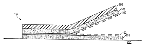
Figure 1 is a schematic illustration of the general
design of a tamper indicating RFID label according to an
embodiment of the invention. Figure 1 shows schematically a
-6-
CA 02417616 2003-O1-28
WO 02/11094 PCT/USO1/23639
pressure sensitive (i.e. self-adhesive) label 100 in cross
sectional view. The label 100 may include four functionally
distinct layers.
The RFID layer 101 may be a layer, which includes RFID
components, for example, an RFID memory chip. The label 100
may in some embodiments provide an "active" RFID capability,
in which case the layer 101 can also include a battery or
other power source.
The second layer 102 may include one or more thin
electrically conducting tracks which should be coupled to
the RFID components in the layer 101. The tracks are known
herein as "tamper tracks" since they provide a means to
detect tampering with or removal of the label 100 from a
surface to which it has been applied.
The layer 101 and the layer 102 may together provide an
RFID capability. On the other hand, in some embodiments the
layer 101 can provide an RFID capability in its own right,
while the tamper tracks 102 can modify the RFID performance.
of the layer 101 depending on whether said tamper tracks 102
are damaged or not.
The RFID capability provided by the layer 101, or the
layers 101 and 102 together, usually includes the ability to
store information in the RFID memory chip in the layer 101,
and the ability to read and modify said stored information
from a distance. Additional capabilities, such as the
ability to encrypt stored information or control access to
the stored information, may also be provided.
The third layer 103 may be an adhesive layer, which in
some embodiments is a pressure sensitive adhesive.
The fourth layer 104 is a top-coat layer applied over
the top of the RFID layer 101. The top-coat may be applied
to protect the RFID layer and to provide a top surface to
CA 02417616 2003-O1-28
WO 02/11094 PCT/USO1/23639
accept a printing process. The top-coat layer 104 is not
essential and in some embodiments may not be included. The
finished construction is the adhesive label 100.
The tamper tracks 102 should be destructible. When
the label 100 is applied to a surface and subsequently
tampered or removed, the pressure sensitive adhesive 103
damages the tamper tracks 102 - for example, by tearing
all or part of them from the underside of the layer 101
which in turn affects the RFID performance of the label
100. Since the tamper tracks 102 are electrically
connected to the RFID components in the label 100, and may
form part of the RFID components of the label 100, the
RFID function of the label 100 is modified if the label is
applied to a surface and subsequently tampered or removed.
In this way tampering with or removal of the label 100 can
be detected at a distance via the change in the RFID
characteristics and response of the label 100.
The terms "tampering" and "tampered" as used herein
refer to complete or partial removal of a tamper indicating.
label, such as the label 100, from a surface to which it has
been applied.
In this document the term "destructible" is used in
relation to the tamper tracks 102 in figure 1 and in
relation to other tamper tracks throughout the document.
In this context the term destructible means that the
tamper tracks are designed to be damaged or broken in
regions of the label which are tampered.
The term "conductive track" is defined herein as any
circuit feature conducting electricity. Tamper tracks,
destructible electronics, antennae and through hole
interconnects are all forms of conductive tracks.
_g_
CA 02417616 2003-O1-28
WO 02/11094 PCT/USO1/23639
The tamper tracks 102 may be produced in one of a
number of different ways. In one preferred embodiment, the
tamper tracks may be produced by printing electrically
conducting ink (such as a carbon/graphite based conductive
ink or a precious metal ink). In another preferred
embodiment the tamper tracks 102 may be produced using
electrically conductive adhesive. Tn another embodiment
the tamper tracks may be metallic tracks made of Aluminum,
Copper or some other suitable metal.
In general the tamper tracks 102 should be made from
a material, such as an electrically conducting ink, which
has appropriate electrical properties but which does not
have high intrinsic physical strength. In this way the
tamper tracks 102 can be more easily disrupted or damaged
as the label 100 is partially or completely removed from a
surface to which it has been applied.
In some preferred embodiments the destructibility of
the tamper tracks 102 may be enhanced by including a thin
layer of a suitable adhesion modifying coating on the
underside of the layer 101 either between the layer 101
and the tamper tracks 102, or between the tamper tracks
102 and the, adhesive 103. At least a part of the tamper
tracks should contact the adhesive 103. The layer of
adhesion modifying coating may be applied as a uniform
layer, or in a specified pattern, or in some other manner
such that the properties of the adhesion modifying coating
vary across the layer 101. In some embodiments multiple
layers of adhesion modifying coating may be applied to
"fine tune" the properties of the final composite adhesion
modifying coating.
Inclusion of a adhesion modifying coating between the
RFID layer 101 and the tamper tracks 102 results in the
-9-
CA 02417616 2003-O1-28
WO 02/11094 PCT/USO1/23639
adhesion of the layers to each other being greater or less
in a particular region according to whether the adhesion
modifying coating is present or absent in that region.
Similarly, inclusion of an adhesion modifying coating
between the tamper tracks 102 and the adhesive layer 103
results in the adhesion of the layers to each other being
greater or less in a particular region according to
whether the adhesion modifying coating is absent or
present in that region. Usually, but not necessarily, the
adhesion modifying coating reduces the adhesion of two
layers, which it separates, so that the two layers can be
more easily separated.
The relative adhesion between the layer 101, adhesion
modifying coating, tamper tracks 102 and adhesive layer
103 can be adjusted so that when the label 100 is applied:
to a surface and subsequently tampered or removed, the
tamper tracks 102 are damaged in a pattern corresponding
to the pattern of the adhesion modifying coating. In some
embodiments the tamper tracks 102 may be physically
separated in a pattern corresponding to the pattern of the'
adhesion modifying coating, with some of the tamper tracks
102 remaining on the layer 101 and the remainder of the
tamper tracks 102 remaining on the adhesive layer 103.
This damage to the tamper tracks 102 may affect the RFID
performance of the label 100.
The adhesion modifying coating may be a layer of
lacquer, or a layer of tamper indicating varnish (for
example, similar to that used in some visual tamper
indicating label constructions), or a layer of some other
suitable material formulation.
The tampering indicating characteristics of one
preferred embodiment of the label 100 are illustrated in
-10-
CA 02417616 2003-O1-28
WO 02/11094 PCT/USO1/23639
figure 2, which shows the label 100 in cross section view
before and after removal from a surface 201. Figure 2
illustrates in particular the physical disruption of the
tamper tracks 102 during tampering or removal of the label
100. In figure 2A the label 100 is shown before removal
from the surface 201. Here the tamper tracks 102 are
intact and the label 100 exhibits its normal RFID
operation. In figure 2B the label 100 has been partially
removed from the surface 201. As the label 100 is removed,
portions of the tamper tracks 102 remain with the top
layer 101, and complementary portions of the tamper tracks
102 remain with the adhesive layer 103. The differential
separation of the tamper tracks 102 may in some
embodiments be enhanced or achieved through the inclusion
of an adhesion modifying coating (as described above) in a
specified pattern at the interface between the layer 101.
and the tamper tracks 102, such that the tamper tracks 102
bond less strongly to the layer 101 where the adhesion:
modifying coating has been applied and therefore in such
regions the tamper tracks 102 remain with the adhesive
layer 103 when the label 100 is removed from the surface
201. As the label 100 is removed from the surface 201, the
tamper tracks 102 are damaged, and their electrical
properties are thereby affected. This in turn affects the
RFID properties of the label 100, since the tamper tracks
102 are electrically connected to the layer 101 which
includes RFID components. In figure 2 the separation of
(i.e. damage to) the tamper tracks 102 during tampering of
the label 100 is shown to form a regular repeating
pattern. It should be appreciated that the pattern of the
separation may instead be irregular and may be on a larger
or smaller scale relative to the size of the label 100 or
-11-
CA 02417616 2003-O1-28
WO 02/11094 PCT/USO1/23639
the RFID components in the label 100 than shown in figure
2.
A preferred embodiment of the tamper tracks 102 will
now be described with reference to figure 3, which shows an
embodiment of the RFID label 100 in cross sectional view
(figure 3A) and looking from below through the adhesive
layer 103 at the tamper tracks 102 (figure 3B). In figure 3
the RFID layer 101 has two "through-connect" electrical
connection points, 301 and 302, where the electrical
circuitry in the RFID layer l01 is connected to the
underside of the layer 101. In this embodiment the
electrical connection between the points 301 and 302 by
means of the tamper track 102 should be intact in order to
maintain normal RFID operation of the label 100.
Preferably the tamper track 102 may be disrupted even
if only a portion of the label 100 is tampered. In figure 3
the tamper track 102 runs around the perimeter of the
underside of the layer 101 between points 301 and 302. The.;
configuration for the tamper track 102 illustrated in figure
3 ensures that tampering of even a small portion of the
label 100 will result in a break in the tamper track 102 and
therefore a break in the electrical connection between the
points 301 and 302, which in turn modifies the RFID behavior
of the label 100.
It should be appreciated that other configurations of
the tamper track 102 could also be employed. For example, in
some embodiments the tamper track 102 may form all or part
of an antenna, in which case the points 301 and 302 may not
be electrically connected to each other via a single tamper
track 102.
An RFID label will generally include an electronic
memory chip connected to either an induction loop or an
-12-
CA 02417616 2003-O1-28
WO 02/11094 PCT/USO1/23639
antenna. The induction loop or antenna may enable
communication and data exchange with a remote reading
device. (It should be appreciated that different types of
antenna design may be employed.) Other electrical or
electronic components may also be included in an RFID label.
An active RFID label will include an on-board power source
such as a battery.
Preferred embodiments of ways in which the tamper
tracks 102 can be configured on the underside of the RFID
layer 101 and coupled to the RFID layer 101 will be now be
described by way of non-limiting example. It should be
appreciated that in some embodiments the tamper tracks 102
may be designed to be destructible in some regions and
durable in other regions. For example, the tamper tracks
102 may include some sections, which are durable and
rugged, joined by sections which are destructible.
The .tamper tracks 102 may be connected in one of
several different ways to the RFID layer 101, depending on
the design and operation of the RFID layer 101. Several non-
limiting examples are listed below.
1. The tamper tracks 102 may be connected in series
with an induction loop or antenna in the layer 101.
2. The tamper tracks 102 may constitute all or part of
the induction loop or antenna of the label 100.
3. The tamper tracks 102 may be part of a tamper-
sensing electrical circuit in the label 100, which is
separate from the induction loop or antenna of the label
100.
Figures 4 to 7 are schematic illustrations of further
preferred embodiments of the tamper indicating RFID label
100, showing both a cross sectional view and a view looking
-13-
CA 02417616 2003-O1-28
WO 02/11094 PCT/USO1/23639
from below through the adhesive layer 103 at the tamper
tracks 102.
Figure 4 is a schematic illustration of a preferred
embodiment in which the tamper track 102 connects the points
301 and 302 and is in series with an induction loop 401 in
the RFID layer 101. The RFID layer 101 may include the
induction loop 401 and other components 402, which may be
passive or active. For example, the components 402 in one
embodiment may be a capacitor which, with the induction loop
401, forms a resonant electrical circuit. Alternatively, the
components 402 may include a passive electronic memory chip
for storing data. The tamper track 102 should be intact for
the RFID label 100 of figure 4 to be operational. When the
label 100 is tampered, the tamper track 102 is broken and
the RFID function of the label 100 can be disabled or
modified. In this way it can be determined whether or not'
the label 100 has been tampered. An adhesion modifying
coating may be included, as described above, to enhance
destructibility of the tamper track 102.
Figure 5 is a schematic illustration of another
preferred embodiment in which the tamper track 102 forms an
induction loop 501 for the RFID label 100. In figure 5 .the
through-connect points 301 and 302 are connected to the RFID
components 402 in the layer 101. In connecting the points
301 and 302, the tamper track 102 forms a number of loops,
with the overall layout of the tamper track 102 acting as an
induction loop. Tampering or removing the label 100 results
in a break in the tamper track 102, thereby disabling or
modifying the RFID function of the label 100. In this way it
can be determined whether or not the label 100 has been
tampered. An adhesion modifying coating may be included, as
-14-
CA 02417616 2003-O1-28
WO 02/11094 PCT/USO1/23639
described above, to enhance destructibility of the tamper
tracks 102.
Figure 6 is a schematic illustration of another
preferred embodiment, which is a variation on the embodiment
of figure 5. In figure 6 the tamper tracks 102 form an
antenna, whereas in figure 5 the tamper track 102 forms an
induction loop. The principal difference is that in figure 6
the points 301 and 302 are not connected together by a
single tamper track 102. Instead there are two tamper tracks
102, one starting at point 301 and the other starting at the
point 302. The two tamper tracks 102 form an antenna. In
figure 6 a so-called meander antenna is illustrated,
although it should be appreciated that other forms of
antenna may also be employed. In some antenna designs the
points 301 and 302 may be connected to each other by the
tamper track 102. In figure 6 the through-connect points 301.
and 302 are connected to the RFID components 402. Tampering
the label 100 should result in damage to at least one of the'
tamper tracks 102, thereby affecting the characteristics of
the antenna and modifying or disabling the RFID function of
the label 100. In this way it can be determined whether or
not the label 100 has been tampered. An adhesion modifying
coating may be included, as described above, to enhance
destructibility of the tamper tracks 102.
Figure ~7 is a schematic illustration of another
preferred embodiment, based on the embodiments of figures 5
and 6. The principal difference between the designs
illustrated in figures 5 and 6, and the design illustrated
in figure 7 is that in the design of figure 7 the RFID
components 402 are on the underside of the layer 101. In
some embodiments the RFID components 402 may comprise only
an RFID memory chip, in which case in the design of figure
-15-
CA 02417616 2003-O1-28
WO 02/11094 PCT/USO1/23639
7, both the RFID memory chip 402 and the tamper tracks 102
are on the underside of the layer 101. The tamper tracks are
designed to be destructible, as described herein. An
advantage of the design of figure 7 compared with the
designs of figures 5 and 6 is that in the design of figure 7
there is no need for through-connects to the bottom side of
the layer 101, since the RFID memory chip is on the bottom
side of the layer 101. In the design of figure 7 the tamper
tracks 102 may form an induction loop, as in the design of
10. figure 5, or may form an antenna, as in the design of figure
6. In figure 7 an antenna is shown. An adhesion modifying
coating may be included, as described above, to enhance
destructibility of the tamper tracks 102.
In order to provide an additional indicator of
tampering, the label 100 may be designed to show visual.
evidence of tampering if the label is removed from a surface
to which it has been applied. Visual tamper indication can
be achieved in several ways. In one embodiment a thin
colored layer is applied to the underside of the RFID layer
101. A pattern of adhesion-modifying layer may be applied to
the underside of the colored layer. The adhesion-modifying
layer may be the same layer or a layer in addition to the
adhesion modifying coating described above. The presence of
the adhesion-modifying layer modifies the adhesion of the
colored layer to the adhesive layer 103 such that when the
label 100 is removed from a surface to which it has been
applied, the colored layer breaks up. Areas of color may
adhere to the adhesive layer 103 and other complementary
areas of color may adhere to the RFID layer 101. An
alternative to this embodiment is to apply a pattern of said
adhesion modifying layer directly to the underside of the
RFID layer 101 and apply said thin colored layer to the
-16-
CA 02417616 2003-O1-28
WO 02/11094 PCT/USO1/23639
underside of said adhesion modifying layer. In another
embodiment, the adhesion modifying coating may be applied
directly to the underside of the RFID layer 101 and a
colored adhesive can be used as the adhesive layer 103. In
this case, when the label is removed from a surface to which
it has been applied, the colored adhesive 103 should break
up and areas of the colored adhesive may adhere to the RFID
layer 101 and complementary areas of the colored adhesive
103 may adhere to the surface. It should be appreciated that
other methods may be used to produce a visual tamper
indicating effect.
When using a visual tamper indicating effect, a portion
of the RFID layer 101 and top coat 104 (if a top coat 104 is
present) should be transparent so the visual effect can be
seen by looking through the RFID layer 101 and top coat 104.
This enables easy inspection of the visual tamper indicating
feature without having to remove the label. The RFID
components in the RFID layer 101, such as a memory chip, may
not be transparent, but should only occupy a small portion
of the surface area.
Tamper Indicating RFID Label with Tracking Capability
Figure 8 is a schematic illustration of another
preferred embodiment in which the tamper track 102 forms
part of a separate tamper indicating electrical circuit. As
shown in figure 8 the RFID layer 101 may contain an
induction loop or antenna 801 and other electronic
components 402, including an electronic memory chip, to
provide an RFID capability. The RFID layer 101 should be
capable of interacting with an RFID reading device to allow
reading of or modification to data stored in the electronic
-17-
CA 02417616 2003-O1-28
WO 02/11094 PCT/USO1/23639
memory chip. The through-connect points 301 and 302 are
connected to the components 402 in the layer 101, and to
each other via the tamper track 102. The components 402
should be configured to respond differently to a signal from
an RFID reader depending on whether or not the points 301
and 302 are connected to each other via the tamper track 102
or not. If the tamper track 102 is intact, the label 100
will respond in a specified manner to an RFID reader. On the
other hand, if the label 100 is tampered, so that the tamper
track 102 is damaged and the points 301 and 302 are no
longer connected to each other via the tamper track 102, the
label 100 should still respond to an RFID reader but in a
different manner, thereby indicating that the label 100 has
been tampered. In this way the label 100 of figure 8 can
provide an RFID means to (i) determine whether the label 100
is present, (ii) read data from the label 100 and modify
data stored in the label 100, and (iii) determine whether
the label 100 has been tampered. In one preferred embodiment
the components 402 may consist only of a passive RFID
electronic memory chip, and the tamper track 102 forms a
connection, which may be separate from the induction loop or
antenna 801, between two contact points on the memory chip.
An adhesion modifying coating may be applied between the
RFID layer 101 and the adhesive layer 103, in a manner as
described in relation to figures 1 to 7.
In a variation on the embodiments described above,
the components 402 may undergo an irreversible change if
the label 100 is tampered and the tamper track 102 is
damaged, so that even if the tamper track 102 is
subsequently restored, the label 100 will still respond to
an RFID reader with a signal indicating it has been
tampered. In one preferred embodiment the RFID components
-18-
CA 02417616 2003-O1-28
WO 02/11094 PCT/USO1/23639
402 is "active" (i.e. powered) and is configured to test
the integrity of the tamper track 102 either continuously
or at specified intervals. In this embodiment if the RFID
components 402 detect that the tamper track 102 has been
disrupted they may then preferably be configured to record
data to this effect in the electronic memory chip within
the components 402, preferably in a manner which is
permanent and irreversible. Preferably, if the components
402 are active, they may also include a clock. In this
case, the date and time of any tampering of the tamper
track 102 or label 100 may also preferably be recorded
permanently and irreversibly in the electronic memory chip
within the RFID components 402.
A preferred embodiment of the tamper indicating RFID
label configuration of figure 8 will now be described by way
of non-limiting example with reference to the schemati c
illustrations shown in figure 9.
It should be appreciated that the term antenna as used'
below may refer to a conventional antenna or to an induction
loop (which is used as an antenna at some RFID operating
frequencies).
Figure 9 is a schematic illustration of a tamper
indicating RFID label 900 shown in top view (figure 9A),
cross sectional side view (figure 9B), and bottom view
(figure 9C) .
The label 900 may include a substrate layer 901 made
of, for example, polyester or some other suitable material.
On top of the substrate layer 901,electronics to form an
RFID transponder, which provides an RFID function, may be
applied. The electronics may include an RFID electronic
memory chip 902 and an antenna 903. (In figure 9 an antenna
903 in the form of an induction loop is shown.)
-19-
CA 02417616 2003-O1-28
WO 02/11094 PCT/USO1/23639
Figure 9D is a more detailed schematic illustration of
an example of the electrical connections to the electronic
chip 902.
The chip 902 and antenna 903 should provide an RFID
capability, which may include the ability to store
information in the chip 902, the ability to read information
from the chip 902 at a distance using a suitable RFID
device, and the ability to modify information in the chip
902 from a distance using a suitable RFID device.
The chip 902 may include two contact points, or contact
pads, connected to the antenna 903, as illustrated in figure
9D.
Two contact pads on the chip 902 can be connected via
electrical "through-connects" 904 to the underside of the
substrate layer 901. One or both or neither of these two
contact pads may be the same as the contact pads used to
connect the chip 902 to the antenna 903. Figure 9D shows the
through-connects 904 directly beneath the chip 902. It
should be appreciated that other configurations may instead
be used for the through-connects 904. In another preferred.
embodiment, the through-connects 904 are positioned away
from the contact pads on the chip 902, and electrical tracks
on the top surface of the substrate layer 901 connect the
contact pads on the chip 902 to the tops of the through
connects 904.
The two through-connect points 904 on the underside of
the substrate layer 901 are connected to each other by means
of a tamper track 905 which is positioned on the underside
of the substrate layer 901.
A layer of adhesive 906 may also be applied to the
underside of the substrate layer 901 and tamper track 905.
-20-
CA 02417616 2004-07-16
Preferably said adhesive 906 is a pressure sensitive adhesive.
A top layer 907 may be applied over the top of the substrate 901, chip 902
and antenna 903. The top layer 907 can provide protection for these components
and can also provide a surtace to accept printing - for example printing of a
number, a barcode, a logo, or other image.
It should be appreciated that in figure 9 the top view (figure 9A) is a view
looking through the top layer 907, the side view (figure 9B) is a cross
sectional
side view, and the bottom view (figure 9C) is a view looking though the
adhesive
layer 906.
The tamper track 905 is preferably applied to the underside of the
substrate layer 901, along with one or more layers of adhesion modifying
coating
to enhance the destructibility of the tamper track 905. Consequently, if the
label
900 is applied to a surtace and subsequently removed, the tamper track 905
should be broken or disrupted so as to interrupt the electrical connection
between the through-connect points 904 on the underside of the substrate layer
901. Application of the tamper track 905 and any other adhesion modifying
coatings to the underside of the substrate 901 to enhance the destructible
nature
of the tamper track 905 may preferably be carried out as described herein.
The tamper track 905 may be laid out in a number of different
ways on the underside of the substrate layer 901. In the preferred embodiment
illustrated in figure 9, the tamper track runs from one through-connect
point 904 almost all the way around the perimeter of the underside of the
substrate layer 901 and then back to the other through-
-21 -
CA 02417616 2003-O1-28
WO 02/11094 PCT/USO1/23639
connect point, with the outward and return paths of the
tamper track 905 very close together in order to avoid any
electrical induction effects which may interfere with the
antenna 903 positioned above on the upper surface of the
substrate layer 901. The width and thickness of the tamper
track 905 can be adjusted to provide the correct properties
in terms of electrical resistance and physical
destructibility. The path made by the tamper track 905 may
run inside, or outside, or directly beneath the antenna 903,
which in figure 9 is an induction loop. In one preferred
embodiment the tamper track 905 forms a path which is
outside the outer perimeter of the induction loop 903,
thereby ensuring that any disturbance around the perimeter
of the label 900 will cause the tamper track 905 to be
disrupted.
When the label 900 is applied to a surface, the tamper
track 905 is intact and the corresponding contact pads one
the chip 902 are electrically connected to each other. When-
the label 900 is removed or substantially tampered with, the'
tamper track 905 should be broken or disrupted and there
will then be an open circuit between the corresponding
contact pads on the chip 902. When such an open circuit
occurs, the function of the RFID chip 902 or the information
stored in the chip 902 will be modified in a way which can
be detected by an RFID reader.
If the label 900 is passive (i.e. without an on-board
battery or other power source), the~modified chip function
or information can be detected during the first read
operation of the label after the label 900 is removed or
tampered, and the reader (if it has a write capability) can
be programmed to write data back to the chip 902 to indicate
that the label 900 has been removed or tampered. Said data
-22-
CA 02417616 2003-O1-28
WO 02/11094 PCT/USO1/23639
which is written back to the chip 902 to indicate removal or
tampering of the label 900 is preferably permanent and
irreversible, to prevent the memory contents of the chip
being altered back to the original state to disguise the
fact that the label has been moved or tampered. There is
therefore disclosed herein an RFID read/write device capable
of detecting the change in RFID performance of the label 900
when the label 900 is tampered, and writing data back to the
chip 902 within the label 900 to indicate such tampering has
occurred, said data preferably being written into the chip
902 so as to be permanent and irreversible.
If the label 900 is active (i.e. has an on-board battery
or other power source), it can be configured such that any
disruption to the tamper track 905 can be detected
internally within the label 900 without requiring an RFID
read operation. When such disruption to the tamper track 905
is detected internally, the chip 902 can be programmed to
modify its own memory contents to indicate that the label
900 has been removed or tampered. Said modification to the'
memory contents of the chip 902 to indicate removal or
tampering of the label 900 should preferably be permanent
and irreversible, to prevent the memory contents of the chip
being altered back to the original state to disguise the
fact that the label has been moved or tampered.
Hence the label 900 may function as a normal RFID label
when it is first applied to a surface. After is the label is
moved or tampered, the RFID function of the label 900 may be
maintained and information can be read from and written to
the RFID chip 902, while the label also provides an RFID
means to determine that it has been moved or tampered,
-23-
CA 02417616 2003-O1-28
WO 02/11094 PCT/USO1/23639
Achieving Desired Adhesion Characteristics via Adhesion
Modifying Coating Pattern
Controlling the relative adhesion between the layers of
the transponder construction is critical to achieving the
desired performance of the above-described tamper indicating
device. The reasons for this and the methodologies to
achieve are presented by means of a non-limiting example of
a particular preferred embodiment. It is appreciated that
the same concepts presented here apply to other embodiments
as well.
Figure 10 is a schematic illustration of a tamper
indicating RFID label 900 as shown in figure 9. Figure 10A
illustrates a top view of the antenna layer 903 and the RFID
device 902, and figure 10C illustrates a bottom view of the
tamper track layer 905 and the through connects 904. Figure
10B illustrates a side view with the adhesion modifying
layer 1001 specifically shown. In this embodiment, the"~
adhesion modifying layer 1001 is applied to the bottom of
substrate 901, between the substrate 901 and tamper track
905. Additionally, a release liner layer 1002 is shown on
the bottom side of adhesive layer 906. This release liner
layer is typically applied during the fabrication of the
tamper indicating RFID label 900 and subsequently removed
when the said label is applied to an object. The purpose of
the release liner is to carry the RFID label 900 and prevent
the adhesive layer 906 from inadvertently adhering to any
surface prior to the label 900 being applied to a surface or
object.
In the configuration shown in figure 10, the adhesion
modifying layer 1001 is designed such that its adhesion to
the substrate 901 is weaker than that of tamper track. The
-24-
CA 02417616 2003-O1-28
WO 02/11094 PCT/USO1/23639
tamper track will preferably have substantially strong
adhesion to the substrate 901 and to the adhesion modifying
layer 1001. The adhesion of the tamper track 905 to the
substrate 901 will preferably be stronger than the adhesion
of the adhesive layer 906 to the tamper track 905. Hence
when the transponder construction 900 is attached to a
surface and subsequently removed, the adhesion modifying
layer 1001 will fail (i.e., separate) at the interface to
the substrate 901, thereby transferring the adhesion
modifying coating 1001 and portions of the tamper track 905
in contact with the adhesion modifying coating 1001 to the
adhesive layer 906. Where there is no adhesion modifying
coating 1001, the adhesive layer 906 will separate from the
tamper track 905, leaving those regions of the tamper track
905 in contact with the substrate 901.
It is also appreciated that the adhesion of the
adhesion modifying layer 1001 to the substrate 901 must be
sufficiently strong to prevent delamination or separation
between the said layers during the transponder manufacturing
processes, subsequent handling, removal of the release liner
layer 1002 and application to the intended surface. During
the various manufacturing processes, the tamper indicating
transponder 900 is subjected to thermal, mechanical and
other stresses. Examples of these include, but are not
limited to the following: application of subsequent layers,
thermal or radiation exposure, mechanical assembly, die
cutting, splicing, hole formation, slitting, unwinding ,
rewinding. The transponder may also be subjected to thermal
and mechanical stresses during handling and shipping. When
the release liner layer 1002 is removed from adhesive layer
906, a stress is applied to the adhesion modifying coating
layer 1001, the tamper track layer 905 and adhesive layer
-25-
CA 02417616 2003-O1-28
WO 02/11094 PCT/USO1/23639
906. The relative adhesion between these said layers must
be sufficiently strong as to prevent delamination between
any of them during the removal of the release liner layer
1002.
The adhesion of the adhesion modifying layer 1001 to
the substrate 901 can be controlled by the formulation of
the adhesion modifying material, as will be discussed in a
following section of this patent, as well as by the features
of the release coating layer 1001 pattern. Examples of
these features include, but are not limited to the
following: regions containing geometric shapes of solid
areas of adhesion modifying coating, regions containing
geometric shapes completely absent of adhesion modifying
coating, and regions containing an alternating pattern of
geometric features with and without adhesion modifying
material.
Figure 10D illustrates an example of a preferred
embodiment of the adhesion modifying layer 1001 pattern as
viewed from the bottom of the tamper indicating RFID label
900 through the adhesive layer 906 (not shown) and release
liner layer 1002 (not shown).
It can be seen from figure 10D that the adhesion
modifying layer 1001 , pattern contains the following
features: a grid pattern comprised of lines and spaces, a
solid border at the perimeter of the substrate layer 901,
relatively large regions absent of any adhesion modifying
coating. Each of these features is now discussed in further
detail.
In the referenced example, the grid pattern is
comprised of lines and spaces, oriented at an angle relative
to the perimeter of the substrate layer 901. It is
appreciated that there are many angles at which the pattern
-2 6-
CA 02417616 2003-O1-28
WO 02/11094 PCT/USO1/23639
may be oriented relative to the perimeter and/or the tamper
track. Angles of 90°, 45 ° and 22.5 ° are examples. The
angle affects the printing of the adhesion modifying layer
during manufacturing as well as the release (destruction)
characteristics during application. The width of the lines
and spaces can be varied to adjust the dimensions of the
area of substrate 901 covered by the adhesion modifying
coating layer 1001 versus the dimensions of the area of
substrate 901 in direct contact with the tamper track layer
905. A relatively large area of substrate 901 in direct
contact with the tamper tack layer 905 (low adhesion
modifying coating density) will produce a relatively strong
adhesion between these two layers and therefore generate an
overall construction more resistant to inadvertent
delamination while simultaneously less susceptible to
destruction of the tamper track layer 905 in the
application. Conversely, a relatively large area of~
substrat a 901 covered by adhesion modifying coating layer.
1001 (high adhesion modifying coating density) will generate
an overall construction more susceptible to inadvertent
delamination but also more likely to result in the intended
destruction of tamper track layer 905 in the application.
In addition to a grid, other adhesion modifying coating
patterns can employed, including but not limited to patterns
of lines, dots, and other geometric shapes with the adhesion
modifying coating, with the same or different shapes in the
regions with adhesion modifying coating. It is appreciated
that the dimensions of the regions with material may be
different from those without material. Patterns of lines,
circles and triangles have been tested. The table below
provides a non-limiting example of grid patterns, which have
been evaluated:
-27-
CA 02417616 2003-O1-28
WO 02/11094 PCT/USO1/23639
Line Width Gap Width Orientation of grid
(inches) (inches) to tamper track
0.020 0.020 Orthogonal (90/0
)
0.020 0.030 Orthogonal (90/0
)
0.020 0.040 Orthogonal (90/0
)
0.020 0.020 Angled (22.5)
0.020 0.030 Angled (22.5)
0.020 0.040 ~ Angled (22.5)
The destructibility of layers 1001 and 905, and the
level of adhesion between the label 900 and the surface to
which it is applied, can also be varied across the label 900
by varying the pattern of the adhesion modifying coating
layer 1001, and more specifically by varying the density of
the pattern of the said adhesion modifying coating.
Increasing the density of the adhesion modifying coating
pattern decreases the overall adhesion strength between the ,
label 100 and the surface to which it is applied. For
example, in one preferred embodiment it may be desirable to
have weaker adhesion at the perimeter of the label than at
the center, in which case a higher adhesion modifying
coating density will be employed at the perimeter. In some
instances, the increased density may result in large regions
of solid release coating, such as the solid border of layer
1001 illustrated in figure 10D. Conversely larger areas
without adhesion modifying coating can be employed.
In some preferred embodiments, the adhesion modifying
layer 1001 is applied to the substrate 901 already in the
format of its final dimensions, in that the perimeter of
substrate 901 is the same size as the final product label
900. In another preferred embodiment, the adhesion
modifying layer is applied to the substrate layer 901 having
dimensions larger than the final size of label 900, from
which the label 900 is created via by cutting the substrate
-28-
CA 02417616 2003-O1-28
WO 02/11094 PCT/USO1/23639
901 to the final perimeter dimensions using any one of a
variety of cutting processes (e. g., die cutting, laser
cutting, etc.). In the latter example, the adhesion
modifying coating layer 1001 may be printed larger than
final perimeter dimensions, and the cutting process
therefore cuts through layer 1001 in addition to the
substrate layer 901, thus producing a label 900 with
adhesion modifying coating extending to the perimeter.
Controlling the Fracture Plane via Adhesion Modifyin
Coating Pattern
If the label 900 is applied to a surface which itself
is destructible (for instance, cardboard), the surface can
delaminate resulting in the complete removal of the tamper
indicating label 900 without destruction of the tamper track
layer 906. The destruction properties of the label 900 can
be further enhanced to prevent this situation by adjusting
the pattern of the adhesion modifying layer pattern. Figure
10D depicts relatively large oval shaped regions in layer
1001 absent of adhesion modifying coating. These regions
are positioned diagonally at the four corners and
orthogonally on two sides. It is appreciated that other
shapes, positions and orientations could be employed. If,
for example, the label 900 is applied to a cardboard surface
and later removed, it is possible that the cardboard will
begin to delaminate, with a portion of the cardboard in
contact with the adhesive layer 906. The oval regions in
layer 1001 absent of adhesion modifying coating will
transfer the plane of fracture from within the cardboard to
the intended plane between the adhesion modifying layer 1001
and substrate 901.
-29-
CA 02417616 2003-O1-28
WO 02/11094 PCT/USO1/23639
The use of the adhesion modifying layer pattern to
control adhesion and destruction patterns has been
illustrated using the particular construction of figure 10
wherein the tamper track is located on the opposite side of
substrate 901 from the antenna 903 and the adhesion
modifying layer is applied between the substrate layer 901
and the tamper track 905. It is appreciated that the same
principles apply to the other previously presented
embodiments involving different tamper indicating label
transponder constructions. These include, but are not
limited to, constructions where the tamper track is on the
same side of the substrate as the antenna, the tamper track
may be integral to the antenna, or the release coating is
applied between the tamper track and the adhesive.
Constructions Employing a Transfer Lamination
In one preferred embodiment, the destructible
electronics may be applied to the substrate layer 901 using
a transfer lamination technique. In this method, the
destructible pattern or tamper track layer 905 is created
separately and then transfer laminated to the underside of
the substrate layer 901. A bonding adhesive layer may be
applied uniformly or selectively between substrate layer 901
and tamper track layer 905 to secure the said tamper track
layer to the substrate. The adhesion modifying layer 1001
pattern is preferably applied immediately adjacent to the
destructible electronics tamper track layer 905, either
before or after the application of the tamper track layer
905 to the bonding adhesive. The resulting construction
will produce differential separation of the destructible
electronics upon tampering of the label 900.
-30-
CA 02417616 2003-O1-28
WO 02/11094 PCT/USO1/23639
In one preferred embodiment, the transfer laminated
destructible electronics may be an etched or stamped piece
of continuous metal (e. g., copper, aluminum). In another
preferred embodiment, the transfer laminated destructible
electronics may be a printed electrically conductive
material that may or may not include a polymer binder.
In another preferred embodiment, the bonding adhesive
may be selectively applied in a pattern to the underside of
the substrate 901 such that, after transfer lamination of
the tamper track layer 905, portions of the destructible
layer are not attached by said bonding adhesive to the
substrate 901. In this embodiment, the unattached regions
of the destructible electronics lead to selective failure of
the destructible electronics when the label construction 900
is tampered. In this embodiment, it may not be necessary to
use an adhesion modifying coating.
In another preferred embodiment, the bonding adhesive
is applied uniformly to the bottom side of substrate 901.
In this embodiment, the adhesion modifying layer 1001 is
required.
In another preferred embodiment, the bonding adhesive
layer is applied to the bottom side of layer 901, onto which
the tamper track layer 905 is applied. The adhesion
modifying coating layer is applied between the tamper track
layer and the adhesive layer 906. When applied after
transfer lamination of the destructible electronics, the
adhesion modifying coating inhibits local delamination of
the destructible electronics by the adhesive layer 906 when
the label construction 900 is tampered, since in this
configuration said adhesive modifying coating weakens the
adhesion between the destructible electronics and the
adhesive layer 906.
-31-
CA 02417616 2003-O1-28
WO 02/11094 PCT/USO1/23639
Constructions Involving Multiple RFID Transponders
The Dual-Transponder Tamper Indicating RFID Zabel
Figure 11 is a schematic illustration of the general
design of a dual-transponder tamper indicating RFID label
construction 1100. This second tamper indicating RFID label
is designed such that when tampered it remains operational
in an RFID sense, but provides information, via RFID means,
to indicate that it has been tampered.
Figure 11 shows said second tamper indicating RFID
label 1100 schematically in. cross sectional view.
The label 1100 includes a first RFID layer 1101, which
is a tamper indicating RFID construction of the type
described in relation to figure 1, so that the underside of
the first RFID layer 1101 includes destructible electronics.
A second RFID layer 1102 is bonded in a permanent
manner to the top surface of the first RFID layer 1101. The
layer 1102 includes components to provide an RFID
capability. Said second RFID layer 1102 is preferably
designed to be strong and durable rather than destructible.
The second RFID layer 1102 may be designed to provide a
read-only RFID capability, or a read-write RFID capability,
or some other RFID capability.
To the underside of the first RFID layer 1101 is
applied a layer of adhesive 1103. Preferably the adhesive
layer 1103 will be a pressure sensitive adhesive, although
it should be appreciated that other types of adhesive layer
could be used instead.
Preferably, but not necessarily, a top layer 1104 will
be applied over the top of the second RFID layer 1102. The
-32-
CA 02417616 2003-O1-28
WO 02/11094 PCT/USO1/23639
layer 1104 is included to provide physical protection for
the second RFID layer 1102 and to provide a surface to
accept printing processes (where appropriate).
Due to the properties of the first (bottom) RFID layer
1101, the combined construction of the figure 11 is tamper
indicating, so that an attempt, using methods such as those
described above in relation to figure 1, to partially or
completely remove the label 1100 from a surface to which it
has been applied will result either in a break in the
destructible electronics of the first RFID layer 1101, or
distortion to the destructible electronics, or a disruption
to the connection between the destructible electronics and
the RFID chip in the first RFID layer 1101, or other
modification to the first RFID layer 1101 to the extent that
~ the RFID function of the first RFID layer 1101 is modified
in a manner detectable by an RFID reader or read/write
device. The RFID function of the second RFID layer 1102 will
preferably be~ unaltered by tampering of the label 1100,
since damage due to tampering will usually be confirmed to
the region of the bottom surface of the first RFID layer
1101 and the adhesive layer 1103.
Combining the First and Second RFID payers of the Second
Tamper Indicatinct RFID Zabel.
Figure 12 illustrates schematically ways in which the
first RFID layer 1101 and second RFID layer 1102 of figure
11 can be configured.
Usually the layers 1101 and 1102 of figure 11 will each
include an electronic chip. Typically the chip will be
significantly thicker than the rest of the layer. In the
-33-
CA 02417616 2003-O1-28
WO 02/11094 PCT/USO1/23639
embodiments illustrated in figure 12 the layer 1101 includes
the electronic chip 1201, and the layer 1102 includes the
electronic chip 1202 which is positioned on the top surface
of the layer 1102.
Figure 12A illustrates schematically two cross
sectional views of preferred embodiments of the tamper
indicating RFID label 1100 in which the RFID chip 1201 is on
the top surface of the layer 1101.
In figure 12A(1), the layer 1101 is longer than the
layer 1102, and the chip 1201 is positioned to the side of,
rather than underneath, the layer 1102 so as to allow the
layer 1101 to be bonded evenly to the layer 1102 across the
entire bottom surface of the layer 1102.
In figure 12A(2), the layer 1102 includes a hole and
the layer 1101 is positioned under the layer 1102 such that
the chip 1201 is in said hole, thereby enabling the layer
1101 to be bonded evenly to the layer 1102 across the entire
bottom surface of the layer 1102. The benefit of the designv
of figure 12A(2) is that it provides a more uniform top
surface to the layer 1102, on which top surface a top layer
may be applied.
An adhesive layer 1103 is applied to the bottom surface
of the first RFID layer 1101. Preferably the adhesive layer
1103 is a pressure sensitive adhesive, although it should be
appreciated that other types of adhesive layer could be used
Preferably (but not necessarily) a top layer 1104 may
be applied to the top surface of the second RFID layer 1102.
The top layer 1104 may be applied in order to protect the
layer 1102 and also in order to provide a surface to accept
printing.
Figure 12B illustrates schematically a cross sectional
view of a preferred embodiment of the tamper indicating RFID
-34-
CA 02417616 2003-O1-28
WO 02/11094 PCT/USO1/23639
label 1100 in which the RFID chip 1201 is on the bottom
surface of the layer 1101. Hence the mating surfaces of the
RFID layers 1101 and 1102 are both flat and even, and the
layers 1101 and 1102 can be bonded together across the
entire mating surface of the layers without difficulty.
An adhesive layer 1103 is applied to the bottom surface
of the layer 1101 such that the chip 1201 and destructible
electronics on the bottom surface of the layer 1101 are
sandwiched between the layer 1101 and the adhesive 1103.
Preferably the adhesive layer 1103 is a pressure sensitive
adhesive, although it should be appreciated that other types
of adhesive layer could be used.
Preferably (but not necessarily) a top layer 1104 is
applied to the top surface of the layer 1102. The top layer
1104 may be applied to protect the layer 1102 and also to
provide a surface to accept a printing process.
Transponder Interference
In some circumstances the performance of the RFID layer
1101 and 1102 may be adversely affected by the proximity of
the other layer. This can occur especially when the antennas
or induction loops in the layers 1101 and 1102 are in close
proximity. In order to avoid such effects the antenna or
induction loop in the tamper indicating RFID layer 1101 may
in some preferred embodiments be separated laterally from
the antenna or induction loop in the RFID layer 1102, rather
than being placed directly beneath the antenna or induction
loop in the layer 1102. This is illustrated schematically in
figure 12B, where the antenna or induction loop of the layer
1102 is positioned in the region 1204, while the antenna or
induction loop 1101 is positioned mainly in the region 1203,
-35-
CA 02417616 2003-O1-28
WO 02/11094 PCT/USO1/23639
with some preferred embodiments also including a portion of
the destructible electronics on the bottom surface of the
layer 1101 extending into the region 1204 in order to
provide the tamper indicating function of the layer 1101
across all portions of the label construction 1100.
Use of a Single Substrate Construction
In a variation on the preferred embodiment of figure
12B, the two substrates 1101 and 1102 may be replaced by a
single substrate.
In one embodiment using a single substrate, the durable
transponder may be fabricated directly on the top surface of
said substrate and the destructible transponder may be
fabricated directly on the bottom surface of said substrate.
The destructible transponder may be constructed using any of
the methodologies described herein.
There are manufacturing benefits which result from
having the two electronic chips in said dual-transponder
tamper indicating RFID label on the same side of the single '
substrate layer. This can be achieved as shown in figure 13,
which is schematic illustration of said second tamper
indicating RFID label in which both electronic chips are
positioned on the top side of the single substrate layer. In
figure 13 the electronic chip 1302 of said destructible
transponder is on the top side 1303 of the substrate 1301
and the destructible electronics of said destructible
transponder are on the underside 1304 of the substrate 1301,
with one or more through-connects 1305 connecting the top
and bottom layers 1303 and 1304 of the substrate 1301. A
durable transponder is applied to the top surface 1303 of
the substrate 1301, so that the electronic chip 1306 of the
-36-
CA 02417616 2003-O1-28
WO 02/11094 PCT/USO1/23639
durable transponder is also on the top surface 1303 of the
substrate 1301. An adhesive layer 1307 is applied to the
underside of the substrate layer 1301.
Preferably a top layer 1308 may be applied to the top
surface of the substrate 1301, such that the electronic
chips 1302 and 1306 and any other electronics on the top
surface 1303 of the substrate 1301 are covered over and
protected. Preferably said top layer 1308 may be a layer
designed to accept a printing process.
Preferably, but not necessarily, the two transponders
in the construction illustrated in figure 13 may be
displaced laterally to avoid transponder interference, as
described above.
Mixed Conductor Technology
In a preferred embodiment of the durable transponder
configuration described in relation to figures 11, 12 and
13, the durable transponder and destructible transponder may
be fabricated using two different electrical conductor
technologies. For instance, the durable transponder may be
fabricated using etched metal (e. g., copper or aluminum)
electrical conductors, and the destructible transponder
could be conducted using any of the conductor technologies
described herein.
The Use of Different Transponder Frequencies and Protocols
In a preferred embodiment of the dual transponder
configuration described in relation to figures 11,12 and 13,
the durable transponder and destructible transponder may
operate at different frequencies or use different RFID
-37-
CA 02417616 2003-O1-28
WO 02/11094 PCT/USO1/23639
protocols, or both. Operating the two transponders at
different frequencies offers several potential advantages.
As discussed above, when two transponders operating at the
same frequency are placed in close proximity, the two
antenna coils or induction loops have a de-tuning effect on
each other which can result in the read distance for each
transponder being reduced from the normal operating range.
The magnitude of this effect will depend on the operating
frequency, antenna geometry and position of one transponder
relative to the other. For instance, when two similar
transponders are placed directly on top of each other, the
read distance for each may be substantially reduced. Two
transponders operating at two different frequencies usually
have a lesser de-tuning effect on each other than two
transponders operating at the same frequency. For instance,.
it can be demonstrated that placing a 2.45GHz transponder in
the center of a 13.56MHz transponder coil will have minimal.
effect on the performance of either transponder.
Another potential benefit of using different'
frequencies for the two transponders is reduced label size.
For instance, even when placed adjacent to each other
(rather than on top of each other or one within the other),
a combination of a 2.45GHz transponder and a 13.56MHz
transponder will be smaller than two adjacent 13.56MHz
transponders, simply due to the smaller size of the 2.45GHz
transponder.
The use of two different RFID chip types (with
different RFID protocols) in the dual transponder
construction may also provide certain benefits. In one
preferred embodiment, one chip could be an industry standard
chip while the other could be a custom chip, said custom
chip incorporating enhanced features, functionally or
-38-
CA 02417616 2003-O1-28
WO 02/11094 PCT/USO1/23639
security and being visible (in an RFID sense) only to
especially configured RFID readers. In this case the dual
transponder construction would "look" like a standard single
transponder construction to a standard RFID reader.
The embodiments illustrated and discussed in this
specification are intended only to teach those skilled in
the art the best way known to the inventors to make and
use the invention. Nothing in this specification should be
considered as limiting the scope of the present invention.
The above-described embodiments of the invention may be
modified or varied, and elements added or omitted, without
departing from the invention, as appreciated by those
skilled in the art in light of the above teachings . It is
therefore to be understood that, within the scope of the
claims and their equivalents, the invention may be
practiced otherwise than as specifically described.
Composition of the adhesion modifying coating
The adhesion modifying layer 1001 is comprised of an
adhesion modifying material applied according to the
previously described methodologies. The formulation of the
said material affects the relative adhesion strengths
between the different layers and therefore affects the
performance of the tamper indicating RFID label.
A typical formulation of said adhesion modifying
coating is as follows.
Weight o
Component Range Preferred
Polymer resin or oligomer 5-97 15-65
Diluent 0-80 25-80
Catalyst 0-10 0-7
Filler 0-30 0-20
-39-
CA 02417616 2003-O1-28
WO 02/11094 PCT/USO1/23639
Colorant 0-1.0 0.1-1.0
Flow control additive 0.0-2.0 0.05-1.5
Defoamer 0.01-1.0 0.05-0.5
It should be noted that not all of the above components are
necessarily present in every formulation.
In the above formulation, numerous chemicals may be
utilized for each component. They are selected based on
their adhesion modifying properties for the selected
substrate. Examples of substrate films that can be used
are polyester, polyimide, polyetherimide, polyurethane,
vinyl and paper. Polyethylene terephtalate (PET) films in
varying thickness are preferred. Different types of
resins will have varying levels of adhesion on a
particular substrate. This can be exploited to adjust the
adhesion to the desired level by using blends of polymer
resins or co-polymers whose component parts possess
different adhesion characteristics. For example, the
polymer resin can be a thermoplastic resin such as a
phenoxy resin (for example, PaphenOO PKHC manufactured by
Phenoxy Specialties). Other possible resins include
thermoplastic acrylic, vinyl, polystyrene co-polymers and
polyurethane resins. Thermally cured thermosetting resin
compositions may also be employed. For example, isocyanate
or amino resin crosslinked epoxy, phenoxy, polyester and
vinyl resins, anhydride or amine crosslinked epoxy resins.
In addition to the above, radiation cured formulations
(ultraviolet/visible light or electron beam) can be used,
such as free radical initiated acrylate or methacrylate
systems based on acrylated or methacrylated oligomers. For
example, acrylated or methacrylated epoxy, urethane and
polyester oligomers or cationic initiated systems based on
-40-
CA 02417616 2003-O1-28
WO 02/11094 PCT/USO1/23639
vinyl ethers, epoxies, cycloaliphatic epoxies, epoxidized
oils and rubbers may be used.
The diluent, which is selected based on compatibility
with the chosen resin, the viscosity of the solution, speed
of drying and ease of printing, can be water and/or an
organic solvent. For example, glycol ethers or glycol ether
acetates such as di(ethylene glycol) butyl ether (butyl
carbitol) and di(ethylene glycol) ethyl ether acetate
(carbitol acetate), dibasic esters such as dimethyl adipate,
dimethyl succinate or dimethyl glutarate, gamma
butyrolactone, n-methyl pyrrolidinone, aromatics such as
toluene and xylene, ketones such as methyl ethyl ketone and
isophorone or mixtures thereof, may be used. In the
thermosetting and cationic formulations, the diluent may
include reactive diluents in addition to or in place of the
water or organic solvent, such as low viscosity glycols (for
example, diethylene, triethylene, dipropylene or
tripropylene glycol), polyglycols (for example,
polyethylene, polytetramethylene or polypropylene glycol)
and polyester polyols (for example, Tone~ polyols available
from Union Carbide) . In the case of free radical initiated
formulations low viscosity acrylate or methacrylate monomers
are used. In some instances when using a low viscosity resin
or oligomer the diluent may be omitted entirely.
The thermosetting and radiation cured formulas also
employ a catalyst. In the amino resin cross linked formulas
the catalyst can be a blocked organic or inorganic acid,
such as Nacure~ 2530 manufactured by King Industries.
Epoxy formulations employ catalysts or hardeners such
as anhydrides (for example, Methylhexahydrophthaliic
anhydride), tertiary amine or imidazole catalysts (for
example, Imicure0 AMI-2 manufactured by Air Products and
-41-
CA 02417616 2003-O1-28
WO 02/11094 PCT/USO1/23639
Chemicals), dicyandiamide and amine, amidoamine or modified
amine hardeners (for example, ANCAMINEO 23375 manufactured
by Air Products and Chemicals).
The Ultraviolet/visible light formulas are cured
using free radical or cationic photoinitiators, such as
Irgacure~ 184 manufactured by Ciba specialty chemicals or
Cyracure~ UVI 6992 manufactured by Union Carbide. Electron
beam cured formulasdo not require a catalyst.
Fillers are used alone or in combination to control the
viscosity and rheology of the coating for ease of
application. Inert fillers such as talc, silica, kaolin,
calcium carbonate or barium sulfate may be added.
Thixotropic fillers such as synthetic silica can also be
used (for example, Aerosil~ R-202 manufactured by Degussa).
Flow control additives typically include materials
such as surfactants and leveling agents. These ingredients
contribute to the wetting of the substrate and the quality
of the coating surface.
Typical Flow control additives are modified silicone
oils such as BYK Chemie's BYK~ 323 or non-silicone leveling
agents such as Modaflow~ manufactured by Solutia. Typical
surfactants are fluorocarbons such as FC430 manufactured by
3M or silicone materials such as BYK~ 307. In some cases,
one ingredient (e.g., a surfactant) may provide several of
the effects attributed to the leveling agent, surfactant.
In addition, one or more of the major ingredients (e. g.,
diluent or polymer) might provide the performance attribute
normally provided by these minor ingredients.
Defoamers are chemicals added to control the formation
of foam during mixing and application of the coating. A
typical defoamer is BYK~ 075. In some cases silicone or
-42-
CA 02417616 2003-O1-28
WO 02/11094 PCT/USO1/23639
non silicone leveling agents may provide the performance
attributes of a defoamer or air release agent.
Optionally, colorants such as dyes (e.g organic dyes),
inorganic, organic or organometallic pigments or mixtures,
solutions or dispersions thereof may also be added. For
example, Polytrend~ colorant dispersions manufactured by
Creanova.
The following examples are presented to illustrate, not
limit the invention.
Example 1: Manufacture of the coating
A coating was prepared using the following
ingredients.
Table 2
-Approx.
Component Weight o
Resin
Phenoxy Resin (Paphen~ PKHC) 25.4
Diluent
(Di(ethylene glycol) ethyl ether acetate) 74.1
Defoamer
(BYK~ 075) 0.1
Colorant
(Phthalocyanine Blue 12o dispersion) 0.4
Polytrend~ 850-7240
The phenoxy resin is dissolved in the solvent with
stirring and heating to 50-60 °C. The mixture is cooled to
-43-
CA 02417616 2003-O1-28
WO 02/11094 PCT/USO1/23639
25°C and the defoamer and colorant added. The solution is
further mixed to combine the ingredients.
Example 2. Application of the coating
The coating of example 1 was applied to 0.05mm thick
untreated polyethylene terephthalate film through a
patterned 300 mesh stainless steel screen using standard
screen printing technology.
The screen mesh was selected to produce a dry ink film
thickness (DIET) of between 3 and 7 microns, 4-5 microns
being the typical DIET. Stainless steel or polymer mesh
screens are acceptable. The applied coating was cured in a
conveyor oven at 120° C for 60 seconds.
Alternatively, in the case of a radiation cured formula
a subtractive technique can be used . These formulas are
commonly referred to as photo imagable wherein the coating
is applied as a solid continuous layer. This layer is then .
exposed to the radiation through a mask or phototool
containing the desired pattern. The areas of the coating
where the radiation is not blocked by the mask are cured and
remain intact. The areas of the coating where the radiation
is blocked remain uncured and are subsequently removed by a
developer. Developers are typically organic solvents, water
or aqueous solutions of an inorganic base (for example,
Sodium Carbonate).
It should be apparent to one having ordinary skill in
the art that variations are possible without departing
from the spirit and scope of the invention.
-44-
CA 02417616 2003-O1-28
WO 02/11094 PCT/USO1/23639
Methods to Manufacture of Tamper Indicating RFID Zabel
A preferred method of manufacture of a preferred
embodiment of the invention are illustrated by way of a non-
limiting example using the construction of tamper indicating
label 900 as depicted in figures 10A, 10B, 10C, and 10D. It
is appreciated that the methods described herein are typical
approaches and other methods familiar to those practiced in
the art may also be employed.
Each layer of the transponder design is step and
repeated to create a multi-up layout on large area, such as
18 by 24 inches, in order to economically manufacture
multiple pieces on each sheet of material processed. It is
appreciated that multiple pieces will be processed for each
step described below. It is also appreciated that typical
manufacturing practices will process multiple sheets
sequentially at each process step.
The substrate layer 901 is comprised of Polyethylene
terephtalate (PET) film. The PET film is heat stabilized to
relieve mechanical stresses and reduce dimension instability
as a function of temperature exposure. The holes for the
through connects 904 are then formed by laser, drilling or
punching.
The antenna layer 903 is applied to the top surface of
the substrate 901 by screen printing a conductive polymer
thick film ink (e. g. silver filled ink). The polymer thick
film ink is then thermally cured.
A layer of insulting dielectric is then screen printed
over the antenna layer 903 and UV cured to form the
insulating cross-over layer. . A second layer may be applied
in a similar fashion. A layer of conductive polymer thick
film ink (e.g., silver filled ink) is screen printed on top
-45-
CA 02417616 2003-O1-28
WO 02/11094 PCT/USO1/23639
of the insulating cross-over layer to form the conductive
portion of the cross-over, and then thermally cured. The
filling of the through connect holes 904 may be accomplished
at the same process step or by an addition printing and
curing step. The cross-over layer is consider to be a part
of antenna layer 903.
The adhesion modifying layer 1001 is then applied to
the bottom surface of substrate 901 by screen printing and
thermally curing the adhesion modifying material. The
tamper track 905 is then formed by screen printing and
thermally curing a conductive polymer thick film ink (e. g.,
silver filled ink).
The RFID memory device (usually referred to as an RFID
"chip") 902 is applied to the top surface of the substrate
901 by applying an anisotropic conductive adhesive paste to
the chip location, placing the chip into said paste, and
curing said paste via thermal compression bonding to form
both a mechanical and electrical connection between the chip
902, substrate 901 and antenna 903.
The assembled construction may be tested for
functionality, after which the sheet is cut into strips
which are then spliced together to form a roll of
transponders. The adhesive layer 906 and release liner
layer 1002 are then applied to the bottom of the substrate
901, adhesion modifying layer 1001 and tamper track layer
905. The top layer is then applied to the top of the
substrate 901, over the chip 902 and antenna 903.
It is appreciated that alternative approaches may be
employed at each of the aforementioned process steps and
that entirely different process flow charts and materials
may be employed to obtain a similar end product.
-46-
CA 02417616 2003-O1-28
WO 02/11094 PCT/USO1/23639
It is also appreciated that a tamper indicating
transponder label can be created using an active or passive
RF device. Furthermore, it is appreciated that the
materials, methods and constructions described herein may be
utilized to create tamper indicating circuitry containing
non-RF devices or no discrete electronic devices at all.
-47-