Note: Descriptions are shown in the official language in which they were submitted.
CA 02418674 2003-02-07
TRANMISSION LINES AND COMPONENTS WITH WAVELENGTH REDUCTION AND
SHIELDING
FIELD OF THE INVENTION
[0001] The present invention relates in general to transmission lines and
transmission line
components, in particular novel electric shielding of transmission lines and
components
constructed therefrom.
BACKGROUND OF THE INVENTION
[0002] Faster, silicon-based technologies are driving new applications such as
wireless LAN,
point-to-multipoint distribution, and broadband data services such as gigabit
per second (Gb/s)
fibre-based systems. Shrinking transistor dimensions on-chip has increased
gain-bandwidth
frequencies beyond 200GHz, however, it is widely recognized that passive
components now
limit the speed and frequency range of circuits at RF and higher operating
frequencies. Energy
coupled to the semiconducting substrate in silicon technologies via passive
components is
quickly dissipated. This constrains the gain and bandwidth of monolithic
circuits. Also, at
freqeuncies where wavelengths are shorter than 10mm (i.e., millimeter-wave or
above 12GHz
for signals on a silicon chip) the signal delay over interconnections must be
factored into a
typical integrated circuit design.
[0003] High performance transmission lines and components thereof are
desirable for
interconnections, impedance matching, resonant and distributed circuits, and
for implementing
devices such as signal splitters, hybrid couplers, inductors, arnd balun
transformers.
[0004] One exemplary prior art device is shown in Figure 1, a perspective view
of a portion of
a microstrip transmission line fabricated in silicon technology indicated
generally by the numeral
15. A single top conductor 16 is disposed on an insulator 17 (typicallly
silicon dioxide), a
semiconductor 18 (silicon substrate) and a metal ground plane 19. This forms a
metal-insulator-
semiconductor-metal (MISM) sandwich of insulating dielectric and silicon
layers between the
backside and top-conductor metal 16. While this transmission line is simple,
it suffers from high
energy dissipation into the semiconducting silicon material resulting in pulse
dispersion and
attenuation of the signal being transferred that increases with increasing
frequency.
[0005] Another exemplary prior art device is shown in Figure 2, a perspective
view of a
CA 02418674 2003-02-07
portion of a coplanar waveguide (CPW) on-chip transmission line indicated
generally by the
numeral 20. (As will be described, Figures 1, 2 and 3 are directed to the
prior art and are so
labeled). The coplanar waveguide 20 includes 3 coplanar conductors, a center
conductor 22
with two adjacent ground strips (conductors) 24, 26 in the same plane as the
center conductor
22, all disposed on a silicon substrate 28. The coplanar conductors 22, 24, 26
tend to confine
the electric field to the gap between conductors 22, 24, 26. However, current
crowding along
the conductor edges 22, 24, 26, at higher frequencies causes higher
dissipation than for
microstrip lines.
(0006] A third exemplary prior art device is shown in Figure 3, a perspective
view of a portion
of a simple microstrip transmission line (MIM) indicated generally by the
numeral 30. The
microstrip line includes a strip conductor 32 disposed over an intermetal
dielectric 33 and a
ground sheet 34, followed by an underlying substrate 35.
[0007] The microstrip line 30 includes two layers of metal and therefore has a
relatively large
capacitance per unit length since the intermetal dielectric is generally a few
microns thick. Also,
the ground sheet must be slotted to relieve stress between the metal film and
dielectric for metal
areas larger than about 30x30um2 in typical VLSI (very large scale
integration) interconnect
metal schemes. Leakage of the electromagnetic fields via the slots to the
underlying
semiconductor, and dissipation due to current flow in the metals cause losses
resulting in
decreased performance. These losses are, however, substantially lower than for
the MISM or
CPW transmission lines.
SUMMARY OF THE INVENTION
[0008] In one aspect of the present invention a slow-wave transmission line
component is
provided. The component has at least two conductors, a substrate material
disposed beneath
at least one of the at least two conductors, and a plurality of metal strips
disposed between at
least one conductor of the at least two conductors and the substrate material,
the metal strips
being closely spaced apart such that an electric field from the conductors is
inhibited from
passing the metal strips to the substrate material.
[0009] In another aspect of the present invention a slow-w<~ve inductor is
provided. The
slow-wave inductor has at least one inductor coil layer comprising a metal
strip, a substrate
disposed beneath the inductor coil layer, and a plurality of metal strips
disposed between the at
2
CA 02418674 2003-02-07
least one inductor coil layer and the substrate material, for shielding the
substrate material from
the inductor coil layer.
[0010] In another aspect, there is provided a slow-wave transmission line
component having
a slow-wave structure. The slow-wave structure includes a floating shield
employing one of
electric and magnetic induction to set a potential on floating strips of said
floating shield to about
0, thereby reducing losses caused by electric coupling to a substrate.
[0011] Advantageously, the present invention provides novel transmission lines
with
reduced energy loss to the substrate and reduced chip area for interconnect
structures with a
given wavelength on-chip, compared to conventional microstrip and coplanar
waveguide
transmission lines. In one particular transmission line according to an aspect
of the present
invention, wavelength reduction achieves a Q-factor > 20 frorr~ 20 to 40GHz,
or about three
times higher than conventional transmission lines implemented with the same
technology. An
approximate loss of 0.3dBlmm results, with the wavelength reduced by about a
factor of two
compared to a conventional transmission, thereby minimizing the chip area
consumed by on-
chip microwave devices.
BRIEF DESCRIPTION OF THE DRAWINGS
[0012] The present invention will be better understood with reference to the
drawings, in
which:
[0013] Figure 1 is a simplified perspective view of a portion of a microstrip-
on-silicon (MISM)
on-chip transmission line according to the prior art;
[0014] Figure 2 is a simplified perspective view of a portion of a coplanar
waveguide (CPW)
on-chip transmission line according to the prior art;
[0015] Figure 3 is a simplified perspective view of a portion of a simple
microstrip
transmission line (MIM) according to the prior art;
[0016] Figure 4a is a simplified perspective view of a portion of a slow-wave
coplanar
conductor transmission line in accordance with an embodiment of the present
invention;
[001?] Figure 4b is a simplified top view of a portion of the slow-wave
coplanar conductor
transmission line of Figure 4a;
3
CA 02418674 2003-02-07
[0018] Figure 5 is a graph showing a comparison of measured characteristic
impedance of
the slow-wave coplanar transmission line of Figure 4a with transmission lines
of the prior art;
[0019] Figure 6 is a graph showing a comparison of the measured effective
permittivity of the
slow-wave coplanar transmission Vine of Figure 4a with transmission lines of
the prior art;
[0020] Figure 7 is a graph showing a comparison of the measured quality factor
(Q-factor) of
the slow-wave coplanar transmission line of Figure 4a with trsmsmission lines
of the prior art;
[0021] Figure 8 is a graph showing a comparison of measured attenuation of the
slow-wave
coplanar transmission line of Figure 4a with the transmission Ilines of the
prior art;
[0022] Figure 9 is a simplified top view of a portion of a balanced
transmission line in
accordance with an alternate embodiment of the present invention;
(0023] Figure 10 is a simplified top view of a portion of a coupled
transmission line in
accordance with another embodiment of the present invention;
[0024] Figure 11 is a simplified top view of a portion of a single-ended
transmission line in
accordance with yet another embodiment of the present invention;
[0025] Figure 12 is a simplified top view of a slow-wave symmetric inductor in
accordance
with still another embodiment of the present invention;
[0026] Figure 13 is a simplified top view of a symmetric inductor with slow-
wave interconnects
in accordance with another embodiment of the present invention;
(0027] Figure 14a is a simplified top view of a portion of a slow-wave
coplanar transmission
line according to another embodiment of the present invention;
[0028] Figure 14b is a simplified top view of a first shield portion of the
slow-wave coplanar
transmission line of Figure 14a;
[0029] Figure 14b is a simplified top view of a second shield portion of the
slow-wave
coplanar transmission line of Figure 14a;
[0030] Figure 15a is a simplified top view of a portion of a slow-wave
coplanar transmission
Line according to yet another embodiment of the present invention; and
[0031] Figure 15b is a simplified top view of a shield portion of the slow-
wave coplanar
transmission line of Figure 15a.
4
CA 02418674 2003-02-07
DETAILED DESCRIPTION OF THE PREFERRED EMBODIMENTS
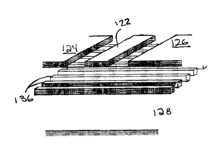
[0032) Reference is made to Figures 4a and 4b to describe a slow-wave coplanar
conductor
transmission line in accordance with an embodiment of the present invention,
and indicated
generally by the numeral 120. ft will occur to those skilled in the art that
the slow-wave coplanar
conductor transmission line 120 has many similarities with the coplanar
conductor 20 of the
prior art, shown in Figure 2. For simplicity, similar parts are denoted by
similar numerals raised
by 100.
[0033] The slow-wave coplanar conductor transmission line 120 (S-CPW) includes
three
coplanar conductors, a center signal conductor 122 with two adjacent ground
strips 124, 126 to
form a coplanar waveguide. A plurality of spaced apart, substantially parallel
metal strips 136
are disposed beneath the signal conductor 122 and the ground strips 124, 126.
Also referred to
as floating strips, the metal strips 136 are not connected to either the
ground strips 124, 126 or
the center conductor 122. These metal strips 136 are very tightly spaced such
that electric field
is inhibited from passing through to the underlying substrate layer. Clearly,
the spacing between
each strip is less than the minimum dimension (width) of the metal strips 136.
The width of
these metal strips is in the direction of the current flow of the signal
conductor 122. In the
present embodiment, the spacing of the of metal strips 136 is .about 1.6
microns. The metal
strips decouple the electric and magnetic field in the vertical dimension from
the conductors, in
the direction of the substrate, to form a slow-wave line. The electric field
is inhibited from
radiating to the semiconducting silicon substrate 128 and the rninimum
dimension (or width) of
the strips 136 is oriented to inhibit current induced via magnetic induction
between the top metal
coplanar conductors 122, 124, 126 and the strips 136.
[0034] It should be noted that although the strip spacing identified in the
present
embodiment is 1.6um, other strip spacings are possible. It is desired to use
as small a spacing
as possible. In future, it is likely that scaling of technologies will allow
much smaller dimesions
(e.g., 0.1 um) to be used. !n the present embodiment, the width of the strips
is chosen as small
as possible, limited by the technology used. It will be understood that for
acceptable
performance, a range of widths could be used with a maximum practical value
for the pitch
between strips of 100 times the spacing between the strips as a guideline.
[0035] A particular implementation of the slow-wave coplanar conductor
transmission line
CA 02418674 2003-02-07
120 will now be described in more detail. This particular implementation is
included for
exemplary purposes only and is not to be construed as limiting the scope of
the present
invention. In the present embodiment, the gap between the center signal
conductor 122 and
each of the ground conductors 124, 126 is relatively wide to achieve a large
line inductance (L).
To maintain the characteristic impedance (Z0) equal to 50 Ohms, the line
capacitance (C) is
increased using a wide center signal conductor 122, and the metal strips 136
are placed
beneath the center signal conductor 122 and the ground conductors 124, 126 to
encourage
capacitive coupling. Since the line inductance L and the line capacitance C
are increased
simultaneously, the speed of a wave travelling along the transmission line is
much lower than
the speed of a wave travelling along a transmission line of they prior art.
This is called a slow-
wave. As a result, the wavelength decreases while the line loss is lowered as
well, and the
energy dissipated per unit length, quantified by the quality factor (Q) of the
transmission line,
improves. The slow-wave coplanar conductor transmission line 120 of the
present embodiment
uses 420 micron tong lower level (LY) shield strips with minimum width
(measured in the same
direction as the current flow along the signal conductors of the top layer),
and spacing between
the strips of about 1.6 microns.
[0036] This novel slow-wave coplanar conductor configuration overcomes many of
the
performance limitations of prior art designs. The physical length of the
transmission lines
required to implement quarter-wavelength microwave devices is reduced as the
electromagnetic
wave velocity is lowered without requiring a change in the dielectric constant
of the surrounding
material. The shorter physical length for implementing quarter-wavelength
microwave couplers
or combiners leads to lower loss and less chip area usage. Also, this
configuration permits a
wider signal line for on-chip 50 Ohm fine implementation to reduce the line
resistance. Further,
the electric field is shielded from the substrate to lower losses at high
frequency.
[0037] Results of testing four transmission line configurations are included
for comparison
purposes. The four transmission tine configurations include the microstrip-on-
silicon (MISM)
transmission line of the prior art, the simple microstrip (MIM) transmission
line of the prior art,
the coplanar waveguide (CPW) transmission line of the prior an, and 'the slow-
wave coplanar
transmission line 120 (S-CPW).
[0038] Characteristic impedance, defined as the ratio of voltage to current at
a given
position, is ideally independent of frequency. All transmission line
configurations tested, except
the MISM line, are designed for a characteristic impedance of 50 Ohms. The
measured
6
CA 02418674 2003-02-07
characteristic impedance ZO for each of the transmission line configurations,
is plotted in Figure
5. As shown, the measured characteristic impedance is close to the design
target with very little
variation with frequency for all transmission lines except the NIISM. The
increase in
characteristic impedance with frequency for the MISM line is related to energy
coupled into the
semiconducting substrate. Within a narrow range of frequencies ZO does not
change
significantly, and power transfer can be maximized by using a load which
matches the
characteristic impedance (i.e., impedance matching). For broader band signals,
such as a non-
return-to-zero binary data stream in a GBit/s fibre-optic system, any changes
in the properties of
the interconnect with frequency causes dispersion and distortion of the
signal. Signal integrity is
improved by shielding the interconnect from the substrate at the cost of
lowering the
characteristic impedance, and therefore both MIM and S-CPV11 lines show
performance
comparable to the reference standard. The reference standard is a commercially
available
CPW line fabricated on an insulating substrate (alumina) using gold metal
conductors. The
losses and Q-factor of the reference standard represent a benchmark for a
transmission line on
a planar substrate.
[0039] Referring now to Figure 6, the wave velocity and wavelength are
inversely
proportional to the effective permittivity (in m/s, where ~r is effective
permittivity) of a
transmission line. The plot of Figure 6 shows effective permittivity as a
function of frequency for
the four transmission lines. Since silicon dioxide is used as the insulator,
the relative permittivity
of the MIM line is approximately 4 over the entire frequency range, as
expected, giving a
wavelength about one-half that of the same signal travelling through air. The
speed of a wave
on an MISM line varies with frequency, decreasing as more energy is coupled
into the substrate.
This causes pulse dispersion, which impairs the risetime in digital circuits.
The S-CPW line
shows much less variation but also an efFective permittivity as high as 20 in
this example,
indicative of wavelength reduction. Note that widening the gap between the
center conductor
122 and the coplanar grounds 124, 126 results in reduced wavelength. A short
wavelength for
a given frequency saves chip area, as the length of transmission line required
to realize a given
phase shift shrinks along with the wavelength. Thus, the S-CP'VV line saves
space resulting in
compact high performance on-chip components.
[0040] As will be understood bar one skilled in the art, the cpality factor (Q-
factor), a
quantifiable quality measurement, is defined as:
Q - Energ s~dJcer c~ ,
7
CA 02418674 2003-02-07
Energy dissipated per cycle
when excited by a sine wave. Energy lost due to dissipation clearly results in
decreased quality
factor.
[0041] The quality (Q) factor for the reference CPW, S-CPW, MIM and MISM lines
are
compared in Figure 7. Dissipation in the reference line (CPU1~~-on-Alumina) is
caused mainly by
ohmic losses in the gold conductors and less by losses in the alumina
substrate and radiation of
the fields. The Q-factor increases almost continually with frequency. Peak Q-
factor values of
40-100 are typical for the CPW transmission line fabricated with gold
conductors on an
insulating substrate (i.e., the reference standard). For the M1;3M line, the Q-
factor initially rises
with frequency, but as more energy is coupled in to the silicon layer, the Q-
factor begins to fall,
reaching a peak of approximately 8 between 3 and 4GHz frequency. This is very
similar to the
behavior of a spiral inductor fabricated on a silicon chip. The MIM structure
almost entirely
blocks energy from the semiconductor layer, but with only a 4 micron
separation between signal
and ground conductors, relatively little energy is stored in the magnetic
field, which limits the Q-
factor. The S-CPW transmission line configuration shields the electric field
and allows the
magnetic field to fill a larger volume, in effect increasing the energy stored
by the transmission
line. This causes a change in wavelength but also a dramatic increase in Q-
factor. The Q-factor
is improved by a factor of 2 compared to the MIM structure fabricated in
copper over most of the
range, and by a factor greater than 3 in the mm-wave range between 30 and
35GHz.
Referring now to Figure 8, a comparison of the measured attenuation per
millimeter length is
provided. The attenuation per millimeter of length is consistent with the Q-
factor data.
[0042] The realization of high-Q components at mm-wave frequencies permits the
realization of higher impedances and therefore higher gain from an amplifier
with a tuned or
narrowband load fabricated using an advanced IC technology. The performance of
the novel
transmission lines implemented on the all copper IC technology compares very
favorably with
the off-chip reference line, which is fabricated using high-quality materials
on an insulating
substrate. The proposed technique of wavelength reduction improves the
quality, lowers the
loss per unit length, and reduces the wavelength of the transmission lines.
This opens the
possibility of compact implementation of microwave couplers and combiners on
semiconducting
silicon substrates for applications such as distributed amplifier:> and power
amplifiers, which are
usually implemented in more expensive technologies that use semi-insulating
substrates (e.g.,
GaAs or InP).
8
CA 02418674 2003-02-07
[0043] It will be appreciated that the present invention may take many forms
and is not
limited to the slow-wave coplanar conductor transmission line 120, as
described in detail above.
[0044] Reference is made to Figure 9 to describe a second embodiment of a
transmission
line of the present invention. Figure 9 shows a top view of a portion of a
balanced or differential
transmission line 220 that includes a pair of coplanar balanced signal
conductors 238, 240 and
a plurality of metal strips disposed beneath the balanced signal conductors
236. It will be
appreciated that the coplanar balanced signal conductors 238, 240 include a
positive phase
signal conductor 238 and a negative phase signal conductor 240. The metal
strips 236 are not
connected to either of the signal conductors 238, 240 and inhibit the electric
field from radiating
to the underlying semiconducting silicon substrate. Again the minimum
dimension (or width, as
measured in the same direction as current flow in the overlying signal
conductors) of the strips
236 is oriented to inhibit current induced via magnetic induction between the
top coplanar
conductors and the strips. It will now be understood that the signal
conductors 238, 240 are
shielded from the semiconducting substrate and the wavelength of this
transmission line is
reduced.
[0045] Reference is now made to Figure 10 to describe a third embodiment of a
transmission
line of the present invention. Figure 10 shows top view of a portion of a
coupled transmission
320 line that includes a first signal fine 342 coupled to a second signal line
344. A plurality of
metal strips 336 are disposed beneath the first signal line 342 and a floating
shield 346 is
disposed beneath the second signal line 344. The plurality of metal strips 336
are not
connected to either the first or the second signal lines 343, 344,
respectively, and inhibit the
electric field from the first signal line 342 from radiating to the
semiconducting silicon substrate.
Similar to the above-described embodiments, the minimum dimension of the
strips 336 is
oriented to inhibit current induced between the first signal line 342 and the
metal strips 336. It
will now be understood that the wavelength of the first signal line 342 is
smaller than the
wavelength of the second signal line 344. Thus, waves travel at different
speeds for in the
different signal lines.
[0046] Reference is made to Figure 17 to describe a fourths embodiment of the
present
invention. Figure 11 shows a top view of a portion of a single ended
transmission line 420 that
is similar to the first described embodiment and includes three coplanar
conductors, a center
signal conductor 422 with two adjacent ground strips 424, 426 to form a
coplanar waveguide. A
plurality of metal strips 436 are disposed beneath the signet conductor and
the ground strips
9
CA 02418674 2003-02-07
436. In the present embodiment, however, the metal strips 436 are connected to
the ground
conductors 424, 426 through electrical vies 448. Thus, in the present
embodiment, the metal
strips 436 are not "floating strips", as in the first-described emk~odiment.
This provides a
transmission line with reduced wavelength.
[0047] Referring now to Figure 12, a fifth embodiment of the present invention
is described.
Figure 12 shows a top view of a symmetric inductor 550 inclucling first and
second terminals
552, 554 designed using a slow-wave transmission line with a plurality of thin
metal strips 536
disposed beneath the top conductor coil and the semiconducting substrate. It
will be
appreciated that the thin metal strips 536 shield the first and second
inductor coils from the
semiconducting substrate, thereby inhibiting losses to the substrate which
contribute to time
average energy loss. This reduction in time average energy loss results in an
increase in the
quality factor (Q-factor) of the inductor.
[0048] Referring to Figure 13, a sixth embodiment of the present invention is
described.
Figure 13 shows a top view of a symmetric inductor with slow-wave
interconnects 650 (or
terminals). The symmetric inductor 650 includes first and second terminals
652, 654 and a
plurality of thin metal strips 636 disposed beneath the first and second
terminals 652, 654. It will
now be understood that the signal terminals are shielded from the
semiconducting substrate,
thereby reducing losses.
[0049] From the fifth and sixth embodiments described herein, it will be
apparent that both
the transmission line interconnects and components constructed from
transmission lines such
as inductor and coupled inductor (i.e., transformer) coils can be shielded.
[0050] Referring now to Figures 14a to 14c, a seventh embodiment of the
present invention
is described. Figure 14a shows a simplified top view of a portion of a slow-
wave coplanar
transmission line including three coplanar conductors, a center signal
conductor 722 with two
adjacent ground strips 724, 726 to form a coplanar waveguide. A first
plurality of spaced apart,
substantially parallel metal strips 736 are disposed beneath the signal
conductor 722 and the
ground strips 724, 726. Also referred to as floating strips, the metal strips
736 are not
connected to either the ground strips 724, 726 or the center conductor 722. A
second plurality
of spaced apart, substantially parallel metal strips 737 are disposed beneath
the first plurality of
metal strips 736. Clearly, the second plurality of metal strips 737 are
laterally offset from the first
plurality of metal strips 736, as showin in Figure 14a. The first plurality of
metal strips 736 are
very tightly spaced such that electric field is inhibited from passing through
to the underlying
CA 02418674 2003-02-07
layer. Similarly, the second plurality of metal strips 737 are very tightly
spaced to inhibit electric
field from passing through to the underlying layer.
[0051] Referring now to Figures 15a and 15b, an eighth embodirnent of the
present
invention is described. Figure 15a shows a simiplified top view of a portion
of a slow-wave
coplanar transmission line (S-CPW) including three coplanar conductors, a
center signal
conductor 822 with two adjacent ground strips 824, 826 to form a coplanar
waveguide. A
plurality of metal strips 836 having a plurality of flanges projecting
therefrom, are disposed
beneath the the signal conductor 822 and the ground strips 824, 826. In the
present
embodiment, the flanges of the metal strips 836 correspond tc~ and fit:
between flanges of an
adjacent one of the metal strips 836. Also referred to as floating strips, the
metal strips 836 are
not connected to either the ground strips 824, 826 or the center conductor
822. The plurality of
metal strips 836 are very tightly spaced such that electric field is inhibited
from passing through
to the underlying layer.
[0052] While the embodiments described herein are direci:ed to particular
implementations
of the present invention, it will be understood that modifications and
variations to these
embodiments are within the scope and sphere of the present invention. For
example, the size
and shape of many of the elements described can vary while :>till performing
the same function.
The present invention is not limited to components fabricated on a silicon
substrate, and other
substrates can be used, such as gallium arsenide, germanium, or the like. The
shield strips can
be made of the same metal as the conductors, or coils, or can be made of
different metals and
have different thicknesses. Also, the present invention is not limited to the
particular component
(e.g., inductor and transformer) shapes described herein. Othier
configurations such as three-
dimensional configurations including three-dimensional coil windings, are
possible as the
present invention is not limited to planar structures. Those skilled in the
art may conceive of still
other variations, all of which are believed to be within the sphere and scope
of the present
invention.
11