Note: Descriptions are shown in the official language in which they were submitted.
CA 02419121 2003-02-14 _,
DARK LAYER FOR AN ELECTROLUMINESCENT DEVICE
PRIORITY CLAIM
[0001 ] This application claims priority from US Provisional Patent
Application
601377,208 filed May 5, 2002, the contents of which are incorporated herein by
reference.
FIELD OF THE INVENTION
[0002] The present invention relates to high contrast electroluminescent
devices
and more specifically relates to high contrast electroluminescent devices with
substantially uniform reflection response of reflected ambieht light over the
spectrum of
visible light and with low heat dissipation.
BACKGROUND OF THE INVENTION
[0003] Display devices have become an important part of human Iife during the
past few decades. Electroluminescent display devices (ELDs) are well known and
are
generally composed of several layers of different materials. They fall into
two main
categories, namely, Inorganic Electroluminescent Devices, often referred to as
TFEL
devices (TFEL) and Organic Electroluminescent Devices (ULED). TFELs are
typically
made from inorganic materials, and OLEDs are made from organic materials.
[0004] These layers essentially consist of a transparent front-electrode
layer, an
electroluminescent layer and a reflecting back-electrode layer. Theyoptionally
consist of
additional layers for current regulation and other functions according to
whether he
device being constructed is based on TFEL or OLED. When a voltage is applied
across
the electrodes, the electroluminescent layer becomes active, converting some
portion of
the electrical energy passing therethrough into light. This light is then
emitted out through
the front-electrode, which is transparent to the emitted light, where it is
visible to a user
of the device.
[0005] Electroluminescent devices have been particularly useful as computer
displays and are generally recognized as high-quality displays for computers
and other
electronic devices used in demanding applications such as military, avionics
and
aerospace where features such as high reliability, low weight, and low power
consumption are important. Electroluminescent displays are also gaining
recognition for
1
CA 02419121 2003-02-14
their qualities in automotive, personal computer and other consumer
industries, as they
can offer certain benefits over other displays such as cathode-ray tubes
("CRT") and
liquid crystal displays ("LCD").
[0006]
However, ambient light poses an undesirable effect on all displays, including
electroluminescent displays. The reflection of ambient light by the display
device screen
can cause low picture contrast, thus reducing the picture quality.
Improvements to the
contrast ratio of an electroluminescent device are generally desirable and
particularly
important in avionics and military applications where poor contrast and glare
can have
serious consequences.
[0007] U.S. Pat. No. 5,049,780 to Dobrowolski teaches a device having such low
reflectance in electroluminescent devices, achieved through the use of
destructive
interference. Dobrowolski includes specific teachings directed to voltage-
driven
inorganic electroluminescent devices, where the electroluminescent layer is
formed of an
inorganic material, and which typically require one or more additional
transparent
dielectric layers to reduce electrical-breakdown of the inorganic
electroluminescent layer.
U.S. Patent 6,411,019 to Hofstra teaches an OLED device having improved
contrast,
which is also achieved through the use of destructive interference. However,
when
making certain embodiments in Dobrowolski and Hofstra, exacting manufacturing
processes can be required to achieve desired results, which can be unsuitable
for certain
current high volume and low costing requirements for some manufacturing
environments.
[0008] WO 00/35028 to Berger et al. and "An organic electroluminescent dot-
matrix display using carbon Layer" Synthetic Metals, May 1997, pages 73-75, by
Gyoutoku et al, teach electroluminescent displays that attempt to reduce
unwanted
ambient light reflections using graphite and carbon layers, respectively.
Since graphite
and carbon are primarily light absorbing materials, these display devices can
have the
undesirable property of over-heating, and overall not provide desired levels
of ambient
light reflection. Another disadvantage of using graphite and carbon is that
these materials
tend to form films that are not mechanically sound; they have a tendency to
rub off.
Further, the thickness of these layers that can be required to achieve desired
levels of
' ambient light reduction can be undesirable when implemented in a
manufacturing
environment.
2
CA 02419121 2003-02-14
[0009] US Patent 6,429,451 to Hung teaches an OI ED device having reduced
ambient light reflection. The OLED structure includes a bi-layer interfacial
structure and
a reflection-reduction layer formed of an n-type semi-conductor having a work
function
greater than 4.0 eV. The reflection-reduction layer recited therein is
typically an
absorbing layer of Zn01_x, which can be difficult to deposit consistently on a
cost-
effective basis in a high-volume manufacturing environment. Furthermore, Hung
lacks
guidance in providing how to control the various layers recited therein to
provide desired
levels of ambient light reduction. In addition, Hung does not provide guidance
how to
influence reflections of ambient light off of the bi-layer structure - i.e.
ambient light
entering the device that never has an opportunity to reach the reflection-
reduction layer.
SUMMARY OF THE INVENTION
[0010] It is therefore an object of the present invention to provide a novel
organic
electroluminescent device that obviates or mitigates at least one of the above-
identified
disadvantages of the prior art.
[0011] In an aspect of the invention there is provided an electroluminescent
device for displaying an image to a viewer in front of the device, comprising:
a front
transparent anode layer and a rear reflecting cathode layer; at least one
organic
electroluminescent layer disposed between the anode layer and the cathode
layer. The
device further comprises at least one dark layer disposed between tl~.e
electroluminescent
layer and the cathode, the dark layer being comprised of a partially
reflective layer, an
absorptive-transmissive layer, and reflective layer.
[0012] In a particular implementation of the first aspect, the device further
comprises a first buffer layer and a hole transport layer disposed between the
anode and
the electroluminescent layer and a second buffer layer disposed between the
electroluminescent layer and the cathode layer.
BRIEF DESCRIPTION OF THE DRAGS
[0013] The present invention will now be described" by way of example only,
with reference to the embodiments shown in the attached Figures in which:
[0014] Figure 1 is a schematic diagram of a cross-section of a bottom emitting
electroluminescent device in accordance with the first embodiment of the
invention; and,
3
CA 02419121 2003-02-14
[0015] Figure 1 a is a schematic diagram of a cross-section of a top emitting
electroluminescent device in accordance with the second embodiment of the
invention.
DETAILED DESCRIPTION OF THE INVENTION
[0016] A bottom emitting electroluminescent device in accordance with the
first
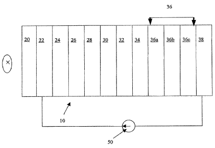
embodiment of the invention is indicated generally at 10 in Figure 1. Device
10
comprises a substrate 20 facing a viewer X, an electroluminescent transmitting
anode 22,
a first buffer layer 24, a hole transport layer 26, an electroluminescent
layer 28, an
electrbn transport layer 30, a second buffer layer 32, a third buffer Layer
34, a dark layer
36 composed of three layers 36a, 36b and 36c, and a reflectir.~g cathode layer
38 disposed
as shown in Figure 1. Device 10 is connected to a current source 50 via anode
22 and
cathode 38 in order to drive a constant current through device 10.
[0017] Substrate 20 is glass, plastic or other transparent material of
suitable
thickness for depositing the layers 22 - 38 using vacuum deposition, spin-
coating or other
means.
[0018] Electroluminescent transmitting anode 22 is any conducting material
which is transparent to at least a portion of emitted electroluminescent
light, such as
indium tin oxide (ITO) or zinc oxide (Zn0). In the present embodiment, anode
22 is a
layer of ITO having a thickness of about twelve-hundred angstroms (1200 A).
Other
suitable materials and appropriate thicknesses can be determined by those
skilled in the
art.
[0019] First buffer layer 24 is made of Cupric Phthalocynine (CuPc) having a
thickness of about two hundred and fifty angstroms (250 A). Other suitable
materials and
appropriate thicknesses can be determined by those skilled in the art. The
function of this
layer is to regulate the hole transportation through the device.
[0020] Hole transport layer 26 is made of N,N'-Di(naphthalen-1-yl}-
N,N'diphenyl-benzidine (NPB; also known as naphthalene diphenyl benzidine),
having a
thickness of about four hundred and fifty angstroms (450 A). Other suitable
materials and
appropriate thicknesses can be determined by those skilled in the art. The
function of this
layer is to facilitate hole transportation through the device.
[0021] Electroluminescent layer 28 and electron transport layer 30 is
typically
deposited as a single layer of an organic electroluminescent material such as
Tris-(8-
4
CA 02419121 2003-02-14
hydroxyquinoline) aluminum) (Alq3) having an appropriate thickness. In the
present
embodiment layer 28 and layer 30 are Alq3 having a combined thickness of about
six
hundred angstroms (600 A) although those of skilled in the art will be able to
determine
other appropriate thicknesses. The function of layer 28 is to emit light,
while the function
of layer 30 is to facilitate hole transport through device 10.
[0022] Second buffer Layer 32 is made from CuPc with an appropriate thickness
as known in the art. In the present embodiment, layer 32. is included to
protect the
elctroluminescent layer during sputter deposition of additional layers of
device 10.
However, where sputter deposition is not used it can be desired to omit layer
32.
[0023] Third buffer layer 34 is made of lithium flour~de (LiF) having a
thickness
of about five to twenty angstroms (5-20 A), but in a presently preferred
embodiment
layer 34 has a thickness of about five angstroms (5 A). Other suitable
materials and
thicknesses can be determined by those of skill in the art. The function of
this layer is to
match the work function of electroluminescent layer 28 and dark layer 36.
[0024] In the present embodiment, dark layer 36 is composed of three layers: a
partially-reflective layer 36a, an absorptive-transmissive layer 36b and a
reflective layer
36c. Layer 36a is made from chromium and is disposed behind buffer layer 34.
Layer 36a
can have a thickness of between about zero to about one hundred angstroms (0-
i00 A).
Layer 36a can also have a thickness of betwveen about zero to about forty
angstroms (0-40
A.). In a presently preferred embodiment, chromium layer 36a has a thickness
of about
twelve angstroms (12 A).
[0025] Layer 36b, disposed behind layer 36a is made from chromium silicon
monoxide preferably having a thickness of between about two hundred to about
eight
hundred angstroms (200-800.A). More preferably, layer 36b can have of
thickness of
between about four hundred to six hundred angstroms (400-600 A). In a
presently
preferred embodiment, layer 36b has thickness of about five hundred angstroms
(500 A).
[0026] Layer 36c, disposed behind layer 36b, is also made from chromium
preferably having a thickness of between about zero to about fifteen-hundred
angstroms
(0 A-1500 A). More preferably, Layer 36c has a thickness of about two hundred
fifty
angstroms (250 A).
[0027] Cathode layer 38 is aluminum (Al) and has a thickness of about fifteen-
hundred angstroms (1500 A), and in the present embodiment it is reflective.
Other
CA 02419121 2003-02-14
suitable materials and appropriate thicknesses can be determined by those
skilled in the
art.
[0028] In a variation of the foregoing embodiment, partially-reflective hyer
36a
is made from aluminum, absorptive-transmissive layer 36b is made from aluminum
silicon monoxide, and reflective layer 36c is made from aluminum. Layer 36a
can have a
thickness of between about zero to about fifty angstroms (0-50 A). Layer 36a
can have a
thickness of between about ten to about thirty-five angstroms (10-35 A). In a
presently
preferred embodiment, aluminum layer 36a has a thickness of about twenty-five
angstroms (25 A). Layer 36b behind layer 36a is made from aluminum silicon
monoxide,
preferably, having a thickness of between about two-hundred-and-fifty to about
five-
hundred angstroms (250-500 A). More preferably, layer 36b is of thickness of
between
about two-hundred-and-seventy-five to about four-hundred-and-fifty angstroms
{275-450
A). More preferably, layer 36b is of thickness of between about three-hundred-
and-
twenty-five to about four-hundred angstroms (325-400 A). In a. presently
preferred
embodiment, layer 36b has thickness of about three-hundred-and-seventy
angstroms (370
A). Layer 36c, disposed behind layer 36b, is another layer of aluminum,
preferably
having a thickness between about 1000 A to about 1500 A. (When layer 36c is
made of
aluminum it is contemplated that cathode layer 38 can be eliminated in favour
of using
layer 36c as the cathode.)
[0029] A wavelength of about five-hundred-and-fifty nanorneters (550 nm), the
centre of the photopic response of the human eye, is the wavelength chosen for
the
purpose of determining appropriate thicknesses and materials of layers 22 to
38, as the
resulting device 10 can have desirable contrast enhancement properties across
the visible
light spectrum. The appropriate thicknesses and materials are chosen to
minimize the
reflection of the device at this wavelength. However, it will occur to those
skilled in the
art that other- wavelengths can be selected, as desired, and the appropriate
material
thickness can be calculated.
[0030] When ambient light is incident upon device 1f7, and passes through
anode
22 and electroluminescent layer 28 towards dark layer 36, at least some of the
ambient
light incident upon dark layer 36 is absorbed thereby and accor~:ingly,
ambient light
reflected back to the viewer X is reduced.
[003 I ] A tap emitting electroluminescent device in accordance with the
second
embodiment of the invention is indicated generally at I Oa in Figure 1 a.
Device 1 Oa
6
CA 02419121 2003-02-14
comprises a substrate 20a (such as glass), a reflecting anode layer 22a, a
dark layer 24a
composed of three layers 24aa, 24ab and 24ac, a first buffer layer 26a, a hole
transport
layer 28a, an electroluminescent layer 30a, an electron transport layer 32a, a
second
buffer layer 34a and electroluminescent transparent cathode 36a as shown in
Figure 1 a.
Device 10a is connected to a current source SOa via cathode 36a anal anode 22a
in order
to drive a constant current through device 10a.
[0032] Electroluminescent transmitting cathode 36a is any transmitting and
conducting material suitable for use in a top emitting OLED device. In a
presently
preferred embodiment, for example, it is contemplated that cathode 36a would
include
three sub-layers consisting of about one-thousand angstroms of ITU, about one-
hundred
angstroms of aluminum and about five angstroms of lithium fluoride. Other
suitable
materials, sub-layers and/or thicknesses can be determined for cathode 36a by
those
skilled in the art.
[0033] Second buffer layer 34a is made from CuPc with an appropriate thickness
as known in the art. The function of this layer is to protect the
elctroluminescent layer
during cathode layer sputter deposition, and could thus be eliminated if other
manufacturing techniques are used.
[0034] Electron transport layer 32a and electroluminescent layer 30a are made
from a single layer of an organic electrolurninescent material. In the present
embodiment
layers 32a and 30a are a single layer of Alq3 preferably having a thickness of
about six
hundred angstroms (600 A) although those of skilled in the art will be able to
determine
other appropriate thicknesses. The function of this single layer is to both
facilitate
electron transport (layer 32a) and to emit light (layer 30a).
[0035] Hole transport layer 28a is made of NPB, preferably having a thickness
of
about four hundred and fifty angstroms (450 A). Other suitable materials and
appropriate
thicknesses can be determined by those skilled in the art. The function of
this layer is to
facilitate hole transportation through the device.
[0036] First buffer layer 26a is made of ITO or Zn0 of an appropriate desired
thickness. Other suitable materials and thicknesses can be determined by those
of skill in
the art. The function of this layer is to work-function match dark layer 24a
with hole
transport layer 28a.
7
CA 02419121 2003-02-14
[0037] Dark layer 24a is composed of three layers: a partially-reflective
layer
24aa, a absorptive-transrnissive layer 24ab and a reflective layer 24ac. Layer
24aa is
made from chromium and is disposed behind buffer layer 26a. Layer 24aa can
have a
thickness of between about zero to about one hundred angstroms (0-100 A). More
preferably, layer preferab24aa can have a thickness of between about zero to
about forty
angstroms (0-40 A). In a presently preferred embodiment, chromium layer 24aa
has a
0
thickness of about twelve angstroms (12 A).
[0038] Layer 24ab, disposed behind, layer 24aa is made from chromium silicon
monoxide preferably having a thiclrness of between about two hundred to about
eight
hundred angstroms (200-800 A.}. More preferably, layer 24ab can have of
thickness of
between about four hundred to six hundred angstroms (400-600 A). In a
presently
preferred embodiment, layer 24ab has thickness of about five hundred angstroms
(500
A).
[0039] Layer 24ac, disposed behind layer 24ab, is also made from chromium
preferably having a thickness of between about zero to about fifteen-hundred
angstroms
(0 -1500 A}. More preferably, layer 24ac has a thickness of about two hundred
fifty
angstroms (250 A).
[0040] Anode layer 22a is aluminum (Al) .and has a thickness of about fifteen-
hundred angstroms (1500 A), and in the present embodiment it is reflective.
Other
suitable materials and appropriate thicknesses can be determined by those
skilled in the
art.
[0041 ] In a variation of the foregoing embodiment, partially reflective layer
24aa
is made from aluminum, absorptive-transmissive layer 24ab is made from
aluminum
silicon monoxide, and reflective layer 24ac is made from aluminum. Layer 24aa
can have
a thickness of between about zero to about fifty angstroms (0-50 A). More
preferably,
layer 24aa has a thickness of between about ten to about thirty-five angstroms
(10-35 A).
Most preferably, aluminum layer 24aa has a thickness of about twenty-five
angstroms (25
A). Layer 24ab behind layer 24aa is made from aluminum silicon monoxide,
preferably,
having a thickness of between about two-hundred-and-fifty to about five-
hundred
angstroms (250-500 A). More preferably, layer 24ab is of thickness of between
about
two-hundred-and-seventy-five to about four-hundred-and-fifty angstroms (275-
450 A).
More preferably, layer 24ab is of thickness of betyveen about three-hundred-
and-twenty
a
five to about four-hundred angstroms (325-400 A). In a presently preferred
embodiment,
8
CA 02419121 2003-02-14
layer 24ab has thickness of about three-hundred-and-seventy angstroms (370 A).
Layer
24ac, disposed behind layer 24ab, is another layer of aluminum, preferably
having a
thickness between about 1000 A to about 1500 A. In this variation, anode layer
22a can
eliminated as layer 24ac can itself act as the anode.
[0042] As known to those skilled in the art, work function matching buffer
layer
26a is not necessary if the dark layer is made of high work function material.
[0043] Those of skilled in the art will now appreciate that the manufacture
and
operation of device 10a is substantially identical to, with appropriate
modifications, the
manufacture and operation of device 10.
[0044] While only specific combinations of the various features and components
of the present invention have been discussed herein, it will be apparent to
those of skill ira
the art that desired sub-sets of the disclosed features and components and/or
alternative
combinations and variations of these features and components can be utilized,
as desired.
Far example, the various buffer layers described herein can be omitted, though
with
commensurate potential for degradation in the operation of the device.
[0045] Other variations will now occur to those of skill in the art, for
example,
substrate 20 could made from a flexible material, such as MylarTM. Where such
flexible
materials are used, it is to be understood that appropriate materials vrill be
chosen for the
other layers in the device - for example, PEI30T from AGFA can be used for the
anode
of the device.
[0046] Furthermore, it is contemplated that other materials can be used for
emitting layer 28 other than AIq3. For example, other types of small-molecule
materials,
other than Alq3 can be used. As an additional example, another type of
emitting material
could be a polymer-based emitting material, such as Polyphenylene vinylene
(PPV). In
such cases it is further contemplated that other materials and. thicknesses
would be used
for the other layers of device 10 to correspond with the features of PPV.
[0047] It is contemplated that certain layers in device 10 that are associated
with
the light emitting functionality of device 10, (i.e. second buffer layer 32,
which can be
used to protect emitting layer 28 during sputtering deposition of other layers
of device
10) can be eliminated and still provide a functional device. In general, it is
to be
understood that the layers of device 10 directed to light ernis:~ion can be
varied and/or be
composed of a different light emitting stack. By the same 'token, the
structure of dark
9
CA 02419121 2003-02-14
layer 36 can be varied to correspond with the particular stack chosen to
effect Light
emlsslon.
[0048] Furthermore, it is to be understood that emitting Layer 28 can be made
doped with different materials, to provide different emitted colours from
layer 28.
[0049] In general, a matrix or (other pattern) of a plurality of devices 10
(or
variations thereof) can be built into a display, whether colour or
monochromatic.
[0050] The devices taught herein can be fabricated using techniques known in
the
art respective to the particular stack of layers and materials that are
chosen. For example,
vacuum-deposited, thermal evaporation or e-beam can be used for non-polymer
materials. Where the device is based on polymer materials such as PPV then
spin-coating
or inkjet printing can be appropriate for the organic materials.
[0051 ] Those of skilled in the art will appreciate the fact that other
mixtures of
metals and ceramics, generally referred to as Cermets, with proper work
function
matching could also be used to fabricate dark layers 36 and 24 in order to
achieve the
desired reflection response. Examples of metals are Al, Cu, Au, Mo, Ni, Pi,
Rh, Ag, W,
Cr, Co, Fe, Ge, Hf, Nb, Pd, Re, V, Si, Se, Ta, Y, and Zr. Examples of oxides
are Al2~3,
5102, Zr02, Hf02, Sc2O3, Tl~2, ITO, La20~, MgO, Ta2~5, T h~2, Y2~3, Ce~2,
Sb2~3, 81203, Nd2~3, Pr6~11, SI~, Zn~, and Gd03.
[0052] Furthermore, it will now be understood by those of skill in the art
that the
dark layer taught herein can be modified to work with inorganic
electroluminescent
structures.
[0053] All documents external to this patent application that are referred to
herein
are hereby incorporated by reference.