Note: Descriptions are shown in the official language in which they were submitted.
CA 02419144 2003-02-06
WO 02/057200 PCT/USO1/41716
TITLE: NANOSCALE MOLECULAR ARRAYER
PRIORITY
This application claims benefit from prior Provisional Application Serial No.
60/225,434, filed August 15, 2000.
FIELD
This invention relates to the generation of solid state molecular arrays. More
specifically, this invention relates to a dedicated apparatus for the creation
of molecular
arrays in a high throughput format with domain sizes as small or smaller than
1 micron in
size.
BACKGROUND
Measuring the binding affinity between materials, molecules, and cells is key
to a
broad spectrum of industries, including material development, semiconductor
production,
bioanalytical assays, biomedical diagnostics, and drug discovery. With the
emergence of
solid state array-based bioanalytical and genetic diagnostic instruments and
related
equipment, new methods for cost effective screening of a large number of
reactions in a
miniaturized solid state form have become increasingly desirable. The favored
approach to
date is to monitor changes in optical properties, usually fluorescence, when a
known,
fluorescently labeled molecule interacts with a known molecular species at a
specific address
in a molecular array. These apparatuses and methods, however, often impose
stereochemical
constraints by the addition of reporter systems to the molecules used to
interrogate the
molecular array. Thus, label free, direct interrogation of molecular binding
events using a
micromechanical reporter is of obvious utility. More sophisticated and robust
instrumentation for the creation of these molecular arrays is therefore
desirable.
CA 02419144 2003-02-06
WO 02/057200 PCT/USO1/41716
One method for the direct detection of molecular interaction events is the
scanning
probe microscope. One type of scanning probe microscope is the atomic force
microscope
("AFM"). In the AFM, a sharp tip is situated at the end of a flexible
cantilever and scanned
over a sample surface. While scanning, the cantilever is deflected by the net
sum of the
attractive and repulsive forces between the tip and sample. If the spring
constant of the
cantilever is known, the net interaction force can be accurately determined
from the
deflection of the cantilever. The deflection of the cantilever is usually
measured by the
reflection of a focused laser beam from the back of the cantilever onto a
split photodiode,
constituting an "optical lever" or "beam deflection" mechanism. Other methods
for the
detection of cantilever deflection include interferometry and piezoelectric
strain gauges.
The first AFMs recorded only the vertical displacements of the cantilever.
More
recent methods involve resonating the tip and allowing only transient contact,
or in some
cases no contact at all, between it and the sample. Plots of tip displacement
or resonance
changes as it traverses a sample surface are used to generate topographic
images. Such
images have revealed the three dimensional structure of a wide vaxiety of
sample types
including material, chemical, and biological specimens. Some examples of the
latter include
DNA, proteins, chromatin, chromosomes, ion channels, and even living cells.
In addition to its imaging capabilities, the AFM can make extremely fine force
measurements. The AFM can directly sense and measure forces in the microNewton
(10-6) to
picoNewton (10-12) range. Thus, the AFM can measure forces between molecular
pairs, and
even within single molecules. Moreover, the AFM can measure a wide variety of
other
forces and phenomena, such as magnetic fields, thermal gradients and
viscoelasticity. This
ability can be exploited to map force fields on a sample surface, and reveal
with high
resolution the location and magnitude of these fields, as in, for example,
localizing complexes
2
CA 02419144 2003-02-06
WO 02/057200 PCT/USO1/41716
of interest located on a specific surface. To make molecular force
measurements, the AFM
probe may be functionalized with a molecule of interest.
Construction of molecular arrays on a solid support for use in an AFM is
typically
carried out by processes that can be divided into two general classes: in situ
and ex situ, the
latter including a mechanical deposition step to actually place the sample on
the deposition
surface. In situ synthesis methods and apparatuses may involve photochemical
synthesis of
nucleic acid or short peptides to define the spatial addresses on a silicon or
a glass surface.
These methods maybe limited by the wavelength of light used for masking and
the synthetic
procedure. Furthermore, this procedure may also be limited by cost. A need
therefore exists
for a dedicated apparatus for the creation of molecular arrays that may create
the array in a
quick and efficient manner.
An example of an ex situ method followed by the mechanical deposition on the
surface may be illustrated by the "dip pen" method. The sample material is
prepared in
advance and then the dip pen is used to place the sample on the deposition
surface. It has
been shown that a dip-pen method may be used to draw a submicron molecular
line or spot
using an alkanethiolate monolayer utilizing a standard AFM to control the dip
pen. Other
prior art instruments may utilize a pin tool which is dipped in a solution
containing the
sample material. The pin tool then has a drop of solution on it, which is then
placed on the
deposition surface. This method, however, does not allow the creation of
extremely small
deposition domains. Up until this time, AFMs have been utilized for drawing
sub-micron
molecular lines or creating the molecular spots. AFMs, however, are not
optimal for creating
arrays because they lack features, such as a sub-micron precision sample stage
under
computer control, precise optical access for sample registration, and
unencumbered access to
the software code used to control the tip motion. Furthermore, commercial AFM
configurations are not amenable to the rapid deposition of large numbers of
different
3
CA 02419144 2003-02-06
WO 02/057200 PCT/USO1/41716
molecular species. Finally, AFMs are designed for multiple tasks, not as a
dedicated sample
deposition instrument, and are therefore more expensive than is required for a
dedicated
arrayer. Still other features may also be desirable in a dedicated deposition
instrument and
not included with an AFM. A need therefore exists for an instrument that is
dedicated to the
creation of arrays comprised of deposition domains.
A need exists for a commercially practical deposition instrument that can be
utilized
to create a molecular deposition array that includes sub-micron deposition
domains. This
instrument may incorporate precise optical features for sample registration
and may be
controlled utilizing a computer control so that user defined array patterns
and sizes may be
created. It may be particularly advantageous if this instrument can operate
autonomously in a
high throughput format.
BRIEF DESCRIPTION OF DRAWINGS
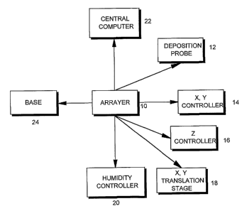
Figure 1 is a block figure representing the various components of the one
embodiment of the present invention.
Figure 2 is a front view of the instrument of one embodiment of the present
invention.
Figure 3a is a perspective view of the X, Y controller of one embodiment of
the
present invention.
Figure 3b is a perspective view of the X, Y translation stage of one
embodiment
of the present invention.
Figure 4 is a perspective view of the deposition probe of one embodiment of
the
present invention.
4
CA 02419144 2003-02-06
WO 02/057200 PCT/USO1/41716
Figure 5 is a block diagram showing the components of the humidity controller
of the present invention.
SUMMARY
An apparatus for creating molecular arrays comprising a base, a Z controller
operably connected to the base wherein the Z controller is selectively
positionable along
a Z axis, a deposition probe removably and operably connected to the Z
controller so
that the deposition probe is selectively positionable along the Z axis by the
Z controller,
an X, Y controller operably connected to the base wherein the X, Y controller
is
selectively positionable along an X axis and a Y axis, the X, Y controller
further
comprising a deposition substrate operably attached thereto and wherein the
movement
of the X, Y controller moves the deposition substrate between a first position
and a
second position, the second position being operably positioned relative to the
deposition
probe, and an X, Y translation stage operably connected to the base wherein
the X, Y
translation stage is selectively positionable along an X axis and a Y axis,
the X, Y
translation stage further comprising a loading substrate operably attached
thereto and
wherein the movement of the X, Y translation stage moves the loading substrate
between a first position and a second position, the second position being
operably
located relative to the deposition probe and the first position being in a
position
accessible by the user.
A method for creating a deposition domain comprising (a) obtaining a loading
substrate, the loading substrate further including a deposition material, (b)
loading the
deposition material onto a deposition probe, and (c) creating a deposition
domain on a
deposition substrate by transferring a desired amount of the deposition
material from
the deposition probe to the deposition substrate.
CA 02419144 2003-02-06
WO 02/057200 PCT/USO1/41716
An apparatus for creating an array comprising, a Z controller, a deposition
probe operably attached to the Z controller, the deposition probe further
comprising a
tip, an X, Y controller operably attached to the Z controller, the X, Y
controller
selectively movable between a first position and a second position, and a
deposition
substrate operably affixed to the X, Y controller wherein when the X, Y
controller
moves the deposition substrate to the second position the deposition substrate
is
operably positioned relative to the deposition probe.
The present invention is a dedicated instrument for the creation of molecular
arrays comprising deposition domains as small or smaller than 1 micron.
Utilizing the
present invention arrayer may limit the use of expensive reagents and test
materials and
may further help to conserve space in large scale combinatorial chemistry
labs. Finally,
the present invention may permit the testing of a large number of samples in a
high
throughput format because of the ease of making custom designed arrays with a
variety
of deposition materials placed thereon.
The present invention apparatus utilizes a deposition technique in which the
sample is transiently hydrated to form a capillary bridge. The capillary
bridge may
transport the deposition material from the loading substrate, to the
deposition probe,
and from the deposition probe to the deposition substrate, to create a
deposition
domain. One or more deposition domains make up the array. The capillary bridge
deposition technique utilized by the present invention apparatus is further
described
herein, and is also described in detail in co-pending U.S. Application
09/574,519, which
is herein incorporated by reference for all that it teaches.
DETAILED DESCRIPTION
6
CA 02419144 2003-02-06
WO 02/057200 PCT/USO1/41716
The specification describes an arrayer 10 that creates arrays comprised of
deposition
domains in a high throughput format. In one embodiment the arrayer is
automatically
controlled, bypassing the need for a user to constantly monitor the formation
of the array. A
general description of the components of the arrayer 10 will be undertaken
followed by a
more specific description of each component.
As illustrated in Figures 1 and 2, one embodiment of the present invention
arrayer 10
may be comprised of a deposition probe 12, an X, Y, controller 14, a Z
controller 16, an X, Y
translation stage 18, a humidity controller 20, a control computer 22, and a
base 24. The
deposition probe 12 may be operably connected to the Z controller 16 which in
turn may be
affixed to the base 24. The X, Y controller 14 may also be affixed to the base
24 on a first
side, of the Z controller 16. The X, Y translation stage 18 may further be
affixed to the base
24 on a second side of the Z controller 16. The humidity controller 20 and the
control
computer 22 may be operably positioned relative to the deposition probe 12,
the X, Y
controller 14, and the X, Y translation stage 18 so that the humidity
controller 20 may
properly perform its respective function, i.e., controlling the humidity. The
computer 22
controls the function of the various components of the present invention
arrayer 10. As may
be appreciated, a number of formations and designs imagined by those skilled
in the art may
be utilized to attach the X, Y controller 14, the Z controller 16, the X, Y
translation stage 18,
etc. to the base 24. Different orientations of the components does not alter
the scope of the
present invention. Furthermore, these components may be attached in a number
of different
ways, including bolting, welding, snapping, etc.
As illustrated in Figure 3a, the X, Y controller 14 further includes a
deposition
substrate 25 movably and removably affixed thereto. The deposition substrate
25 is the
surface upon which the present invention deposits the material. The substrate
is moved by
the X, Y controller 14 into a position underneath the Z controller 16 so that
that deposition
7
CA 02419144 2003-02-06
WO 02/057200 PCT/USO1/41716
probe 12 can be lowered and the deposition material deposited. The substrate
25 may be
affixed to the X, Y controller 14 utilizing snaps, clips, raised contours, or
by other methods
known to those skilled in the art. The details of how the arrayer 10 deposits
the material is
better understood after an explanation of each of the portions of the present
embodiment. In
still further embodiments, one controller may control the movement of the
deposition probe
12 in the X, Y, and Z directions.
The deposition substrate 25 utilized in the present invention apparatus may be
formed
of a variety of materials depending on the nature of the deposited material. A
further
description of such deposition substrates 25 can be found in U.S. Application
09/574,519, but
may be altered or changed without changing the nature or scope of the present
invention
arraying apparatus.
As is further illustrated in Figure 3b, the X, Y translation stage 18 may
further include
a loading substrate 27. The loading substrate 27 may be the surface on which
the deposition
material resides before it is loaded onto the deposition probe 12, and then
onto the deposition
substrate 25, of the arrayer 10. The deposition material may be placed on the
loading
substrate 27 by methods known to those reasonably skilled in the art, such as
by mechanical
deposition, ire situ photochemical synthesis, "ink jet" printing, and
electronically driven
deposition, without changing the nature and scope of the present invention.
In one embodiment, as illustrated in Figure 2, the arrayer 10 may further
comprise a
force feedback monitor 50 and an optical microscope 52. The force feedback
monitor 50
may be operably connected to the deposition probe 12, the Z controller 16, and
the control
computer 22. The force feedback monitor 50 may assist the present invention in
controlling
the height of the deposition probe 12 relative to the deposition substrate 25
and the loading
substrate 27. The optical microscope 52 may be operably attached at a position
below the
base 24 in such a position to aid the user in observing the action of the
arrayer 10.
CA 02419144 2003-02-06
WO 02/057200 PCT/USO1/41716
Each of these separate components of the present invention apparatus will now
be
further described herein.
Base 24
With reference to Figure 2, the base 24 of the present invention will be
herein
described. The base 24 of the present embodiment is physically stable and
provides various
places where the separate portions of the present invention may be mounted.
The base 24 of
the present embodiment may utilize a 12 x 24 inch optical plate supported on
steel posts 26.
The optical plate is a standard platform for building various types of
instrumentation.
One commercially available optical plate 24 that may be well suited for use in
the
present invention arrayer 12 may be available from Newport Corp., P.O. Box
19607, Irvine
CA 92623-9607 as product number SA12. The plate may have 1/a inch holes
drilled on one
inch centers. Steel posts 26 well suited for the present invention may also be
commercially
available from the same manufacturer as product number SP12.
In alternative embodiments, the optical plate may be placed on top of an
optical table.
The optical table can be floated on nitrogen pistons to optimize the
elimination of vibrations,
though in the present embodiment it is not necessary to go to such extremes to
create arrays
with the present invention.
Controller 14
With reference to Figures 2 and 3a, the X, Y controller 14 of the present
invention
will be herein described. As illustrated in Figures 2 and 3a, the X, Y,
control 14 may be
operably attached to the base 24. The X, Y controller 14 should be capable of
microfine and
repeatable movement so that the attached deposition substrate 25 can be
precisely positioned
in a repeatable manner underneath the deposition probe 12. The operative end
of the X, Y
controller 14, as illustrated in Figure 2, may be positioned in such a manner
that the controller
will move the deposition substrate 25 underneath the deposition probe 12 with
micron
9
CA 02419144 2003-02-06
WO 02/057200 PCT/USO1/41716
precision and will also be able to move the substrate 25 out of the way to
allow the X, Y
translation stage 18 to move the loading substrate 27 under the probe 12.
One X, Y controller 14 may be a piezo driven inchworm precision mechanical
stage.
The inchworm mechanism may have a significant range of motion while
maintaining the
microfine precision desirable for the present invention. Such a stage may have
approximately
20 nm spatial resolution in the X and Y planes and may further utilize
encoders to ensure
repeatability. The stage may be fitted with a plate designed by those skilled
in the art to hold
the sample deposition substrate 25. One inch worm stage that may be useful is
commercially
available from Burleigh Instruments, Burleigh Park, P.O. Box E, Fishers, N.Y.
14453-0755.
In an alternative embodiment, a piezo driven flexure stage may also be
utilized as the
X, Y controller 14. A piezo driven flexure may have essentially the same
precision as the
inchworm stage. In still a further embodiment, a linear piezo ratchet
mechanism, such as is
available from NanoMotion, Israel, may be utilized. Figure 2 illustrates an X,
Y controller 14
with a separate motor for the X and Y direction, although various designs may
be utilized.
X, Y Translation Stage 18
With reference to Figures 2 and 3b, the translation stage 18 may be further
herein
described. The X,Y translation stage 18 is operably attached to the base 24 in
a position
relative to the Z controller 16 and the deposition probe 12 such that it
operably interacts with
the same. In the present embodiment, the operative end of the X, Y translation
stage 18 is
fitted with a loading substrate 27 pre-constructed with one or more deposition
materials
placed thereon. The loading substrate 27 may be operably affixed to the X, Y
translation
stage 18 in much the same manner as the deposition substrate 25 is attached to
the X, Y
controller 14. As illustrated in Figures 2 and 3b, the X, Y translation stage
may be positioned
such that the loading substrate 27 can be moved into an operable position
underneath the
deposition probe 12.
CA 02419144 2003-02-06
WO 02/057200 PCT/USO1/41716
In one embodiment, the X, Y translation stage 18 may utilize the same type of
X, Y
positionable inchworm or piezo device as the X, Y controller 14. In
alternative embodiments
the X, Y translation stage 18 may not require such microfine control since the
deposition
material may be placed in a much larger, and therefore easily accessible,
domain on the
loading substrate 27 compound with the domain created on the deposition
substrate 25. As
illustrated in Figure 2, the present embodiment X, Y translation stage 18 may
have much the
same design as the X, Y controller 14.
In further embodiments, the X, Y translation stage 18 may have such a range of
motion that the loading substrate 27 can be loaded in a first position and
then transported into
a second position underneath the deposition probe 12. In this manner, the
loading substrate
27 may be cleaned and reloaded with a second deposition material after the
first deposition
material is loaded onto the probe, all in an automatic fashion.
Z Controller 16
With reference to Figure 2, the Z controller 16 of the present invention will
be herein
further described. The Z controller 16 may be operably attached to the base 24
where it can
operably interact with the X, Y controller 14 and the X, Y translation stage
18. The Z
controller 16 may freely move in the vertical (Z) direction. The Z controller
16 of the present
invention preferably has an accuracy of 200 nm or less in the Z direction so
that the arrayer
may be able to accomplish repeatable and consistent deposition domains in a
high
throughput format. It may also be preferable for the Z controller 16 to have
lateral
repeatability of one micron or less so that the present invention can create
high density arrays
with as little as 1 to 2 microns, or less, of space between each spot on the
array, i.e., the pitch.
In one embodiment, the Z controller 16 may be commercially available from
Newport
Corporation, P.O. Box 19607, Irvine, CA 929623-9607, product number TSV 150.
In this
present embodiment, the Z controller 16 stays relatively stationary in the X,
Y direction,
11
CA 02419144 2003-02-06
WO 02/057200 PCT/USO1/41716
allowing the X, Y controller 14 and the X, Y translation stage 18 to move the
substrates 25,
27 into position. In alternative embodiments, the Z controller 16 may have X,
Y mobility
without changing the nature and scope of the present invention.
Deposition Probe 12
As illustrated in Figures 2 (fixed to the end of the Z controller 16, but not
visible in
Figure 2) and 4 the present invention deposition probe 12 may be further
described herein.
The deposition probe 12 is preferably 100 to 200 microns long and has a tip 13
of roughly 1-
20 microns in height. The radius of curvature of the tip 13 may be
approximately 10-50 nm.
In one embodiment the probe is modified with a 5-10 micron diameter sphere
mounted on the
end of the cantilever. The manner in which the sphere can facilitate loading
of the probe 12
and deposition of the deposition material may be further described in the
above referenced
patent application. Furthermore, the operative attachment of such a probe 12
to a Z controller
16 is well known to share in the art and need not be described here.
A commercially available probe may be utilized as the deposition probe 12 of
the
present invention. Such a probe may be a standard silicon nitride AFM probe
available from
Digital Instruments/Veeco, 112 Robin Hill Road, Santa Barbara, CA.
Humidity Controller 20
As illustrated in Figures 2 and 5, the humidity controller 20 of the present
invention
will be herein described. As illustrated in Figure 2, the controller 20 may be
operably affixed
to the base 24. As illustrated in Figure 5, the humidity controller 20 may
further comprise a
humidity source 30, a gas flow monitoring and control apparatus 32 (not shown)
a gas source
38, a first solenoid valve 40, a second solenoid valve 42, and interconnective
tubing 44. The
humidity source 30 may be operably positioned to effectively and accurately
control the
humidity around the deposition probe 12 during the loading and deposition of
the deposition
material. The monitoring system 32 may be positioned between the humidity
source 30 and
12
CA 02419144 2003-02-06
WO 02/057200 PCT/USO1/41716
the deposition probe 12 and controlled by the computer 22. The gas source 38
may be
operably connected to the first solenoid 40 and the humidity source 30 by the
tubing 44. The
gas source may be further connected to the second solenoid 42 by tubing 44
bypassing the
humidity source. Furthermore, as shown in Figure 2, tubing 44 may channel the
gas to the
probe 12. The humidity controller 20 of the present invention may allow for
the reproducible
deposition of samples in sub-micron and nanometer domains.
The humidity source 30 of the present embodiment utilizes a wetted piece of
filter
paper or a sponge in a plastic cartridge. A dry inert gas, such as argon, is
placed into the
cartridge from the gas source 38 and kept under a positive pressure though the
use of the
solenoid valve 40 controlled by the control system. As illustrated in Figure
5, the gas is
discharged by the humidity controller 20, through the solenoid valve 40 and
the humidity
source 30, past the monitoring and control approaches 32 to flow over the
deposition probe
12 and to increase the relative humidity around the probe 12 in such a manner
as to effectuate
the loading or deposition of the deposition material.
As illustrated in Figure 5, the second solenoid 42 may also draw gas from the
gas
source 38, but route the gas through tubing 44 that goes around the plastic
cartridge 36 and
then to the monitoring and control apparatus 32. In this manner, dry gas may
be delivered to
the deposition probe 12. The solenoid 42 is controlled by the computer 22 and
the
monitoring apparatus 32 in such a manner that dry gas is mixed with humid gas
to achieve
the desired humidity level before reaching the probe 12. Furthermore, after
the deposition
material is placed on the deposition probe 12, or the deposition substrate 25,
the dry gas
solenoid 42 may be used to blast dry gas over the deposition probe to dry the
deposition
material on the probe 12 or on the deposition substrate 25. As may be
appreciated, the output
from the solenoids 40, 42 may be routed through the monitoring apparatus 32
attached to the
monitoring system 32 so to improve repeatability and optimal deposition
conditions for
13
CA 02419144 2003-02-06
WO 02/057200 PCT/USO1/41716
various deposition materials. A numerical value may be assigned to each flow
rate;
monitoring and variations of this numerical value may aid in achieving the
desired humidity
levels.
In alternative embodiments, a more sophisticated humidity generator may be
utilized
so that the present invention can further increase the precision and
repeatability of the relative
humidity surrounding the sample. In yet another embodiment, the dry air may be
continuously blown over the deposition probe 12, briefly stopped during the
wet gas blast,
and then immediately turned on again to minimize sample diffusion on the
surface.
In still another embodiment, a constant, humid environment may be adequate for
sample loading and deposition. For this embodiment, the present invention may
include a
plastic chamber or room that envelopes the deposition probe 12, the operative
ends of the X,
Y controller 14, and the X, Y translation stage 18, or the entire instrument.
The chamber or
room may be filled with a gas of the desired humidity for the duration of the
loading and
deposition program.
Control Computer 22
With reference to Figures 1 and 2, the control computer 22 will be herein
described.
The control computer may be a standard computer utilizing a Pentium, Athlon,
or other
computer chip with a standard operating environment that includes a monitor,
hard drive, etc.
The present embodiment may utilize a standard data acquisition computer board
commercially available from National Instruments, 11500 Mopac Expressway,
Austin, TX
78759-3504, product number PCI-6025e. Such an acquisition board may compile
the
necessary data to control the humidity, the height of the deposition probe 12,
the relative
positions of the Z controller 16, the X, Y controller 14, the X, Y translation
stage 18, and
may also monitor the positions that the deposition material is placed on the
deposition
substrate 25. Standard or customized software may be loaded onto the computer
22 and may
14
CA 02419144 2003-02-06
WO 02/057200 PCT/USO1/41716
control the operation of the data acquisition board. Customizable software of
particular use
may be available from LabView.
In addition to the computer controller 22, a stepper motor controller card (A-
100 from
Mill-Shaf Technologies, Inc.) may be utilized to control the fine action of
the N, Y controller
14, the Z controller 16, and the X, Y translation stage 18. The stepper motor
controller card
of the present embodiment may also be controlled by the LabView (National
Instruments)
software or other software written by those skilled in the art.
Force Feed Back Monitor 50
With reference to Figure 2, the force feed back monitor 50 may be further
described
herein. As previously noted, the force feed back monitor 50 may be operably
attached to the
Z controller 16 and the control computer 22. The force feed back monitor 50
may be able,
along with the control computer 22, to accurately recognize when the
deposition probe 12
and the loading substrate 27, or the deposition probe 12 and the deposition
substrate 25 touch.
Knowing the exact moment of contact between and probe 12 and the substrate 25,
27 may
more accurately allow transferal of the deposition material from the loading
substrate 27 to
the deposition probe 12 and from the deposition probe 12 to the deposition
substrate 25. A
force feed back monitor 50 coupled with the control computer 22 may be known
to those in
the art for achieving such a result.
In alternative embodiments, the force feed back monitor 50 may only be used to
determine the initial relationship of the substrates 25, 27 and the probe 12.
Utilizing the present invention arrayer 10 the probe 12 may be brought into
contact
with the substrate 25, 27 and then drawn back up to 1 mm or more before being
exposed to
the humid gas which causes the capillary bridge to form, thus loading or
depositing the
deposition material. Once the position of the substrate 25, 27 is determined
relative to the
probe 12, the computer 22 may simply bring the probe 12 to the desired level
above the
CA 02419144 2003-02-06
WO 02/057200 PCT/USO1/41716
substrate 25, 27 for the subsequent depositions without having to touch the
surface of the
substrate 25, 27.
Various types of force feed back monitors 50 useful for the above may be known
to
those skilled in the art.
One commercially available force feed back monitor may be an AFM head from a
Dimension 3100 series scanning probe microscope available from Digital
Instruments. Other
force feed back monitors may be utilized by those of reasonable skill in the
art without
changing the nature and scope of the present invention. In the present
embodiment, the read-
out of the monitor 50 may be read through a standard break-out box and fed
directly into
LabView. In operation, a deflection value may be established as the threshold
value at which
LabView will stop the Z controller 14. Thus, once the surface is "found," the
instrument of
the present invention may be programmed to move the Z controller 14 to within
200nm of the
same position repeatedly. In this manner, the instrument may approach and
retract from the
surface rapidly without the necessity of slowing and carefully counting steps
until contact is
made on each deposition cycle.
Optical Microscope 52
With reference to Figure 2, the optical microscope 52 may be further herein
described. As illustrated in Figure 2, the optical microscope 52 is mounted
underneath the
optical plate in an inverted position. The optical microscope 52 allows the
user to visualize
the loading and deposition steps from below the deposition probe 12. Such
monitoring may
be within the resolution limits of the far field optics of a standard
microscope that includes
10X, 20x, 40x, and 60x magnification options with a lOx eyepiece. In still
further
embodiments, such a microscope may be fitted with a camera for image output to
the
computer 22, to a separate monitor or to a recording device. As may be
appreciated by those
16
CA 02419144 2003-02-06
WO 02/057200 PCT/USO1/41716
skilled in the art, the microscope may be excluded from the present invention
arrayer 10
without changing the nature and scope of the invention.
Although the deposition domains may be smaller than the wavelength of the
light
being used, they are separated by distances on the order of 2 microns,
allowing them to be
separately observed by virtue of their optical characteristics. This is
analogous to far field
optical observation of sub-wavelength objects such as individual DNA molecules
and
manometer scale colloidal metals by virtue of light collected from
intercalated fiuorophores
or reflected photons, respectively. This, optical monitoring may be a useful
method for
preliminary evaluation of the deposition event as performed by the present
invention.
Method of LTse
The method of use of the present embodiment will now be herein described. The
Z
controller 16 is used to bring the probe 12 into contact, or near contact,
with the loading
substrate 27. Contact force is regulated by monitoring the cantilever
deflection signal in
LabView through the force feed back monitor 50. A blast of humid gas is then
utilized to
create a capillary bridge between the probe 12 and the loading substrate 27.
This capillary
bridge transfers some amount of the deposition material to the probe 12. The
deposition
probe 12 is then withdrawn using the Z controller 16. The loading substrate 27
is then moved
by the X, Y translation stage 18 out of position beneath the probe 12. The X,
Y controller 14
then moves the deposition substrate 25 into position underneath the probe 12.
The probe 12
is then brought down into position by the Z controller 12 and the humidity
cycle repeated to
deposit the deposition material on the deposition substrate 25.
As may be appreciated, this process may be earned out many times before the
deposition probe 12 is significantly depleted of deposition material. Thus,
one to several
deposition domains for each array can be constructed after loading the probe
12 just one time.
17
CA 02419144 2003-02-06
WO 02/057200 PCT/USO1/41716
Each time a new deposition material is deposited, the deposition probe 12 is
cleaned. In one
embodiment, the probe 12 may be cleaned with UV or ozone burst before loading
a second
deposition material.
In one embodiment, a sample of protein at a concentration of about 0.1 mg/ml
in PBS
(a buffered saline solution) may be deposited as a microdrop on a clean glass
surface and
dried to serve as the deposition materials/loading substrate. The deposition
tool may be
allowed to contact the dried microdrop and the humidity controlled to allow
adsorption of
protein to the deposition probe tip 13. This process typically results in
loading of the
deposition tool with sufficient material fox 10 to 100 deposition events. The
loaded
deposition probe 12 is then utilized to deposit the PBS onto a freshly
prepared gold or
gold/alkanethiolate surface.
Each cycle of loading the probe and making one domain on the deposition
substrate
may take as little as 1 minute. In addition, the actual deposition event is
relatively short, so
the difference between making one and several spots with a single source
material is only a
few seconds at most. Thus, to build one, or many 10 x 10 molecular arrays of
100 different
molecular species may take approximately 1 hour and 40 minutes. In alternative
embodiments, this process may be further streamlined and scaled up to allow
construction of
much more complex arrays (hundreds to thousands of molecular species), and
larger numbers
of arrays in a similar time frame, without changing the nature and scope of
the present
invention. All of these steps may be coordinated through LabView utilizing the
computer 22.
In still further embodiments, there may be several X, Y translation stages 18
to bring
loading substrates 27 into an operable position underneath the deposition
probe 12. In this
manner multiple deposition materials can be accessed on the multiple loading
substrates 27,
allowing for the creation of an extremely diverse array.
18
CA 02419144 2003-02-06
WO 02/057200 PCT/USO1/41716
In yet another alternative embodiment, the optical microscope 52 may be
utilized to
locate registration marks for sample deposition in defined physical locations.
In another embodiment, the probe may be washed using a microfabricated well
with a
simple fluidic feed. The washing solution (e.g., water) may be fed into the
device, forming a
protruding bubble held in place by surface tension. The deposition tool may
then be washed
in the bubble by piezo driven oscillation of the bubble in the probeiz.
As will be appreciated by those skilled in the art, spot size will be a
function of the
radius of curvature of the deposition tool, tool and surface
hydrophobicity/hydrophilicity, and
the control of humidity during the deposition event. The present invention may
allow spot
sizes in the 200 nm diameter range (tool radius is typically 40 nm)
reproducibly when the
appropriate parameters are carefully monitored. It is noteworthy that spots
quite a bit smaller
than this may be possible depending on the sample material and the purposes
envisioned for
the deposition domain.
The information and examples described herein are for illustrative purposes
and are
not meant to exclude any derivations or alternative methods that are within
the conceptual
context of the invention. It is contemplated that various deviations can be
made to this
embodiment without deviating from the scope of the present invention.
Accordingly, it is
intended that the scope of the present invention be dictated by the appended
claims rather
than by the foregoing description of this embodiment.
19