Note: Descriptions are shown in the official language in which they were submitted.
CA 02419570 2005-07-25
'7 9212-4
1
POWER CIRCUIT AND METHOD FOR CONTROLLING SAME
BACKGROUND OF THE INVENTION
1. Field of the Invention
The present invention relates to a power circuit and a method
for controlling the power circuit being capable of making a peak
value of a source current adapted to supply source power to a load
in which its power consumption changes periodically and of allowing
an amount of a current drain to exceed an upper limit value within
a set period of time.
2. Description of the Related Art
In recent years, as terminals of portable devices become
multifunctional to achieve connections or access to the Internet,
distribution of moving pictures, or a like, both a transmission
speed and an amount of data communications tend to increase.
Moreover, it is essential that these terminals of portable devices
be made not only multifunctional but also smaller and more
lightweight from a viewpoint of convenience for use.
On the other hand, as terminals of portable devices become
multifunctional, an amount of power being consumed tends to
increase and therefore it is required that a cell being used as
a power source has a large capacity. However, such a large capacity
CA 02419570 2003-02-19
2
of a cell serving as a power source leads to a larger scale of
and a larger weight of terminals of portable devices, which become
contradictory to a demand for being made smaller and lightweight
being required for terminals of portable devices to improve
performance.
To satisfy such demands being contradictory to each other
in terminals of portable devices, a cell having higher energy
density or having lower internal impedance is being developed,
however, such presently available contrivance does not achieve
a satisfactory result. Moreover, development of technology to
enhance discharge efficiency of a cell is being subject to review.
In the case of terminals of portable devices, in many cases,
performance of a cell is evaluated by using operating time of
portable devices as a specified value. Here, the operating time
refers to elapsed time during which portable devices can be operated
normally and is defined as time being elapsed before a voltage
of the cell reaches a lowest value of a voltage that can drive
portable devices.
To improve discharge efficiency of a cell, matching between
a lowest voltage that can drive the above portable devices and
a voltage that terminates discharge of the cell is effective and
therefore methods which enable portable devices to be operated
at a low voltage by using a DC-DC (direct current to direct current)
converter circuit or a like as a power source and which enable
calibration of a discharge terminating voltage of a cell by
optimizing a number of serial cells are conventionally employed.
However, in the case of such portable devices in which their
loads vary with time which is specific to digital devices prevailing
in recent years as devices operating according to a TDMA (Time
CA 02419570 2005-07-25
79212-4
3
Division Multiple Access) method, digital data transfer
systems, or likes, since their cell voltage changes over
time, matching between the lowest driving voltage and the
discharge terminating voltage becomes difficult and
therefore a conventional power source circuit has a problem
in that it cannot operate a cell fully effectively.
Moreover, in the case of devices being supplied
with source power from a personal computer or a like serving
as a host according to a USB (Universal Serial Bus) being
specifications for the Internet, there is a problem in that,
since an upper limit is imposed on a current that can be
employed in the USB, devices that consume a current
exceeding the upper limit can not be used.
Thus, a conventional power circuit presents a
problem in that effective use of a cell serving as a power
source is impossible and devices consuming a current
exceeding such a limit value cannot be used.
SUMMARY OF THE INVENTION
In view of the above, it is an object of the
present invention to provide a power circuit and a method
for controlling the power circuit that enables effective use
of a cell serving as a source power and that is capable of
using devices consuming a current exceeding a limit value.
According to a first aspect of the present
invention, there is provided a power circuit for feeding a
load current to a load in which said load current repeats
periodically and alternately a burst flow in a burst period
and a non-burst flow in a non-burst period comprising: a
power source section made up of a direct current power
source whose one terminal is connected to a negative
polarity; a source power controlling section to control a
7 9212-4
CA 02419570 2005-07-25
4
current fed from said power source section being connected
to an input terminal and to feed said current to a load
being connected to an output terminal; an energy storing
section having a storage capacitor being connected between
said output terminal and a negative polarity; and wherein
said source power controlling section is provided with a
current controlling circuit to control a resistance value of
a detecting resistor whose one terminal is connected to said
negative polarity according to a result of detection of a
voltage input from said power source section and a switching
circuit which has a circuit part made up of a switching
device being connected between an input terminal and an
output terminal and a capacitor being connected between said
output terminal and a negative polarity and which controls a
flowing period of an output current by exerting control on
said switching device according to a control signal being
produced by detecting a change in an input power voltage
using a voltage value occurring at another terminal of said
detecting resistor.
According to a second aspect of the present
invention, there is provided a power circuit for feeding a
load current to a load in which said load current repeats
periodically and alternately a burst flow in a burst period
and a non-burst flow in a non-burst period comprising: a
power source section made up of a direct current power
source whose one terminal is connected to a negative
polarity; a source power controlling section to control a
current fed from said power source section being connected
to an input terminal and to feed said current to a load
being connected to an output terminal; an energy storing
section having a storage capacitor being connected between
said output terminal and a negative polarity; and wherein
said source power controlling section is provided with a
CA 02419570 2005-07-25
79212-4
current controlling circuit to control a resistance value of
a detecting resistor whose one terminal is connected to said
negative polarity according to a result of detection of a
voltage input from said power source section and a switching
5 circuit which has a step-up DC-DC (direct current to direct
current) converter circuit made up of a voltage detecting
circuit to detect a voltage of an output terminal, a coil
and diode being connected in series between an input
terminal and said output terminal, a capacitor being
connected between said output terminal and a negative
polarity and a switching device being connected between a
connecting point between said coil and said diode and
another terminal of said detecting resistor and which
controls a flowing period of an output current by exerting
control on said switching device according to a control
signal being produced by a signal having detected a change
in a current of said switching device using a voltage value
at said other terminal of said detecting resistor and by a
signal having detected a voltage at said output terminal.
According to a third aspect of the present
invention, there is provided a power circuit for feeding a
load current to a load in which said load current repeats
periodically and alternately a burst flow in a burst period
and a non-burst flow in a non-burst period comprising: a
power source section made up of a direct current power
source whose one terminal is connected to a negative
polarity; a source power controlling section to control a
current fed from said power source section being connected
to an input terminal and to feed said current to a load
being connected to an output terminal; an energy storing
section having a storage capacitor being connected between
said output terminal and a negative polarity; and wherein
said source power controlling section is provided with a
CA 02419570 2005-07-25
79212-4
6
current controlling circuit to control a resistance value of
a detecting resistor whose one terminal is connected to an
input terminal according to a result of detection of a
voltage input from said power source section and a switching
circuit which has a step-down DC-DC converter circuit made
up of a voltage detecting circuit to detect a voltage of an
output terminal, a switching device and a coil being
connected in series between another terminal of said
detecting resistor and said output terminal, a capacitor
being connected between the output terminal and said
negative polarity and a diode being connected between said
negative polarity and a connecting point between said
switching device and said coil, and which controls a flowing
period of an output current by exerting control on said
switching device according to a control signal being
produced by a signal having detected a change in an input
current based on a voltage across said detecting resistor
and by a signal having detected a voltage at said output
terminal.
In the foregoing, a preferable mode is one wherein
a circuit constant of the source power controlling section,
electro-static
CA 02419570 2003-02-19
7
capacity and internal resistance of the storage capacitor are
determined by following equations:
Tl + T2 ~ Tload
where "T1 + T2" denotes a flowing period (Sec) of a power current
and "Tload" denotes a load period (Sec).
Vo / 2 ? IC x ~Rc + (Tload x Don) / (C x 100)} - Vo3
where "VO" denotes a voltage (V) of the storage capacitor occurring
at time of no load, "IC" denotes a current (A) of the storage
capacitor, "RC" denotes an internal resistance ( Sa ) of the storage
capacitor, "Don" denotes a duty ratio ( o) of a load, "C°' denotes
a capacity (F) of a storage capacitor, and "Vo3" denotes an amount
of a voltage drop (V) of a storage capacitor voltage occurring
during a burst period.
Also, a preferable mode is one wherein the power source
section is made up of a secondary cell being connected between
an output terminal and the negative polarity and being connected
to a charging power source through a charging circuit, and of a
primary cell being connected to the output terminal and the negative
polarity through a charging preventing circuit used to prevent
charging caused by an output from the charging power source.
Also, a preferable mode is one wherein the power source
section is made up of a secondary cell being connected between
an output of a charging circuit and the negative polarity and being
connected to an output terminal through a charging preventing
switch and of a primary cell being connected between the output
terminal and the negative polarity.
CA 02419570 2005-07-25
79212-4
8
Also, a preferable mode is one wherein the power
source section is made up of a fuel tank, a fuel cell to
generate power using fuel fed from the fuel tank, and a
direct current smoothing controlling section to stabilize a
voltage output from the fuel cell and to feed it to an
output terminal.
Also, a preferable mode is one wherein the power
source section is made up of a current setting resistor to
set a value of an output current, an operational amplifier
to amplify a detected voltage of the current setting
resistor, and a switching circuit to control a power current
according to an output of the operational amplifier.
Also, a preferable mode is one wherein a storage
capacitor in the energy storing section is made up of an
electric double layer capacitor.
Furthermore, a preferable mode is one wherein the
storage capacitor has a capacitor discharging circuit used
to cause a charge of the storage capacitor has a capacitor
to be shorted through a discharging resistor when a
predetermined relation is formed by comparing a terminal
voltage of the storage capacitor with a power voltage.
According to a fourth aspect of the present
invention, there is provided a method for controlling a
power circuit to feed a load current to a load in which said
load current repeats periodically and alternately a burst
flow in a burst period and a non-burst flow in a non-burst
period which has a power source section made up of a direct
current power source whose one terminal is connected to a
negative polarity, a source power controlling section to
control a current fed from said power source section being
connected to an input terminal and to feed said current to a
load being connected to an output terminal, and an energy
CA 02419570 2005-07-25
79212-4
9
storing section having a storage capacitor being connected
between said output terminal and a negative polarity, said
method comprising: a step of controlling a resistance value
of a detecting resistor whose one terminal is connected to
said negative polarity according to a result of detection of
a voltage input from said power source section; and a step
of controlling a flowing period of an output current by
exerting control on a switching device in response to a
control signal being produced by detecting a change in an
input power voltage using a voltage value occurring at
another terminal of said detecting resistor, in a circuit
part being made up of a switching device being connected
between an input terminal and an output terminal and a
capacitor being connected between said output terminal and a
negative polarity.
According to a fifth aspect of the present
invention, there is provided a method for controlling a
power circuit to feed a load current to a load in which said
load current repeats periodically and alternately a burst
flow in a burst period and a non-burst flow in a non-burst
period which has a power source section made up of a direct
current power source whose one terminal is connected to a
negative polarity, a source power controlling section to
control a current fed from said power source section being
connected to an input terminal and to feed said current to a
load being connected to an output terminal, and an energy
storing section having a storage capacitor being connected
between said output terminal and a negative polarity, said
method comprising: a step of controlling a resistance value
of a detecting resistor whose one terminal is connected to
said negative polarity according to a result of detection of
a voltage input from said power source section; and a step
of controlling a flowing period of an output current by
CA 02419570 2005-07-25
79212-4
exerting control on said switching device according to a
control signal being produced by a signal having detected a
change in a current of said switching device using a voltage
value at another terminal of said detecting resistor and by
5 a signal having detected a voltage at said output terminal
in a step-up DC-DC converter circuit made up of a coil and
diode being connected in series between an input terminal
and an output terminal, a capacitor being connected between
said output terminal and a negative polarity and a switching
10 device being connected between a connecting point between
said coil and said diode and said other terminal of said
detecting resistor.
According to a sixth aspect of the present
invention, there is provided a method for controlling a
power circuit to feed a load current to a load in which said
load current repeats periodically and alternately a burst
flow in a burst period and a non-burst flow in a non-burst
period which has a power source section made up of a direct
current power source whose one terminal is connected to a
negative polarity, a source power controlling section to
control a current fed from said power source section being
connected to an input terminal and to feed said current to a
load being connected to an output terminal, and an energy
storing section having a storage capacitor being connected
between said output terminal and said negative polarity,
said method comprising: a step of controlling a resistance
value of a detecting resistor whose one terminal is
connected to an input terminal according to a result of
detection of a voltage input from said power source section;
and a step of controlling a flowing period of an output
current by exerting control on said switching device
according to a control signal being produced by a signal
having detected a change in an input current based on a
CA 02419570 2005-07-25
79212-4
11
voltage across said detecting resistor and by a signal
having detected a voltage at said output terminal in a step-
down DC-DC converter circuit made up of a switching device
and a coil being connected in series between another
terminal of said detecting resistor and an output terminal,
a capacitor being connected between the output terminal and
said negative polarity, and a diode being connected between
a connecting point between said switching device and said
coil and said negative polarity.
With the above configurations, in the power
circuit having a direct current power source as a power
source, by placing an energy storing section on an output
side of the current limiting section adapted to exert output
current control and output voltage control in order to
accommodate a change in the load current, even in the case
of a load in which its current flows periodically and
alternately in a burst-period and a non-burst period, a peak
value of a power current can be made smaller. By making a
peak value of a power current, in the case where the power
source section is a cell, discharging life of the cell can
be extended. Moreover, even in the case of a power source
whose output current has an upper limit value, in the case
of a load in which, though power consumption exceeds an
upper limit value only during a burst period, average power
consumption is less than power supplied from the power
source, the power circuit can be driven. Moreover, in the
case where the load, though consuming a constant power in an
ordinary manner, provides a current pattern in which a burst
period and a non-burst period occur alternately and
periodically, since an
CA 02419570 2003-02-19
z2
upper limit value of a set current can be changed automatically
according to a power voltage, even if the load consumes constant
power, so long as it is a periodical pulse, the effect described
above can be obtained.
Thus, the present invention is related to the power circuit
and the method for controlling the power circuit which can be
suitably employed in a case in which a chemical cell or a power
source whose output current has its upper limit value is used when
a load such as a TDMA-type portable cellular phone is to be driven
in which power consumption changes periodically. The TDMA
communication method includes a PDC (Personal Digital Cellular)
method, a GSM (Global System for Mobile Communication), a GPRS
(General Packet Ratio Service) or a like.
In the TDMA-type portable cellular phone, power consumption
changes periodically in synchronization with driving of a power
amplifier for generating a transmitting wave . Generally, as a power
source for the TDMA-type portable cellular phone, a chemical cell
using an electrochemical reaction or a direct current power source
in which an upper limit value is imposed on its output current
is used. Here, the periodical change in the power consumption
represents that a load current flows in a burst period and in a
non-burst period periodically and alternately.
In the case of using a chemical cell as a power source, when
a load current flows during a burst period, a voltage of the chemical
cell drops due to a voltage drop caused by an internal impedance
in the chemical cell. However, when the load current flows during
the non-burst period, an amount of the voltage drop decreases which
causes a cell voltage to be restored. Such the periodical operation
causes a cell voltage to be changed in a vibration manner. In a
CA 02419570 2003-02-19
13
general device, if a voltage value during the burst period becomes
less than a minimum driving voltage of a device, driving of the
device is made impossible.
The chemical cell includes a primary cell such as a manganese
dry cell, an alkaline dry cell, a lithium battery, or a like, and
a secondary cell such as a lead storage battery, a Ni-Cd alkaline
battery, a nickel-hydrogen cell, a lithium ion cell, or a like,
and further a fuel cell or a like having a mechanism in which power
is generated by causing chemical reaction of oxygen and hydrogen
being fed from an outside.
In the case of a power source whose output current has an
upper limit value, if a burst current value of a load current exceeds
the upper limit value of a permissible current that the power source
provides, an output is not generated by the power source and, as
a result, a device cannot be driven. The power source whose output
current has its upper limit value includes a direct current
stabilizing powersource having an output current limiting function
such as a linear-regulator-type power source, switching-
regulator-type power source, or a like, and a power source whose
maximum current is limited due to current-carrying performance
of an electrical wire which is required for carrying power since
a direct-current power source including a chemical cell is located
in a place being physically apart from the load.
According to the present invention, when a load is driven
in which power consumption is periodically changed, in the case
of using a chemical cell as a power source, it is made possible
to lengthen operation time by improving discharging efficiency
of a cell or, in the case of using a power source whose most upper
output current is limited, even if power consumption of a device
CA 02419570 2003-02-19
14
exceeds an upper limit value within a set period of time, driving
of a device is made possible.
Also; according to the present invention, the above effect
can be improved using a method in which setting of an upper limit
value of a power current is changed.
Moreover, in the case of using a chemical cell as a power
source, a primary cel:L or a secondary cell is used. In this case,
by introducing a charging preventing device to prevent a primary
cell from being erroneously charged, safety required for using
the primary cell can be improved. Two types of units having functions
of controlling a power source can be used in the power circuit
of the present invention, one functioning singly as an output
current limiting device and another functioning as both an output
current limiting device and an output voltage limiting device,
which has improved versatility so as to be able to meet types or
natures of a load.
Furthermore, by introducing a capacitor discharging circuit
adapted to discharge accumulated electric charges in the storage
capacitor to remove residual electric chargesexisting after power
is turned OFF.
BRIEF DESCRIPTION OF THE DRAWINGS
The above and other objects, advantages, and features of
the present invention will be more apparent from the following
description taken in conjunction with the accompanying drawings
in which:
Fig. 1 is a diagram showing a first basic configuration of
a power circuit according to the present invention;
CA 02419570 2003-02-19
Fig. 2 is a circuit diagram for showing a concrete
configuration of the power circuit according to a first embodiment
of the present invention;
Fig. 3 is a time chart illustrating operations of the power
5 circuit according to the first embodiment of the present invention;
Fig. 4 is a diagram explaining an effect of an extension
of a life of a cell in the power circuit according to the first
embodiment of the present invention;
Fig. 5 is a diagram showing a secand basic configuration
10 of a power circuit according to the present invention;
Fig. 6 is a circuit diagram for showing a concrete
configuration of a power circuit according to a second embodiment
of the present invention;
Fig. 7 is a circuit diagram for showing a concrete
15 configuration of a power circuit according to a third embodiment
of the present invention;
Fig. 8 is a circuit diagram for showing a concrete
configuration of a power source section in a power circuit according
to a fourth embodiment of the present invention;
Fig. 9 is a circuit diagram for showing a concrete
configuration of a power source section in a power circuit according
to a fifth embodiment of the present invention; and
Fig. 10 is a circuit diagram for showing a concrete
configuration of a power source section in a power circuit according
to a sixth embodiment of the present invention;
DETAILED DESCRIPTION OF THE PREFERRED EMBODIMENTS
Best modes of.carrying out the present invention will be
CA 02419570 2003-02-19
16
described in further detail using various embodiments with
reference to the accompanying drawings.
First Basic Configuration
A power circuit of the present invention has two basic
configurations. Figure 1 is a diagram showing a first basic
configuration of a power circuit according to the present invention.
The power circuit having the first configuration of the present
invention; as shown in Fig. l, chiefly includes a power source
section 1, a power controlling section 2, and an energy storing
section 3. The power controlling section 2 is made up of a current
controlling circuit 4 and a control switching device 5. The power
source section 1 is made up of a direct current power source . The
power controlling section 2 is used to control a current output
from the power source section 1 and includes a current controlling
circuit 4 adapted to produce a control signal to be used for
controlling a current output from the power source section 1 arid
a control switching device 5 adapted to control a current output
from the power source section 1 according to a control signal fed
from the current controlling circuit 4 . The energy storing section
3 stores part of electric energy fed from the power source section
1, which is obtained after having undergone current control by
the power controlling section 2 and supplies power to a load 6.
First Embodiment
Next, detailed configurations of the power circuit having
the first basic configuration are further described.
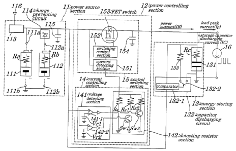
Figure 2 is a circuit diagram for showing a concrete
CA 02419570 2003-02-19
17
configuration of the power circuit of the first embodiment . Figure
3 is a time chart illustrating operations of the power circuit
of the first embodiment. Figure 4 is a diagram explaining an effect
of an extension of a life of a cell in the power circuit of the
first embodiment.
The power circuit of the first embodiment, as shown in Fig.
2, chiefly includes a power source section 11, a power controlling
section 12, and an energy storing section 13 . The power controlling
section 12 is made up of a current controlling section 14 and a
control switching section 15.
The power source section 11 is a direct current power source
using a chemical cell and makes up a cell holder that can house
a secondary cell 111 or a primary cell 112 . The power source section
11 further includes a secondary cell charging circuit 113, a charge
preventing circuit 114, and a capacitor 115. A positive polarity
terminal 111a being connected to a positive polarity of the
secondary cell 111 is connected to an output side of the secondary
cell charging circuit 113 . A negative polarity terminal 111b being
connected to a negative polarity of the secondary cell 111 is
connected to a negative polarity side of the power source section
11. A positive polarity terminal 112a being connected to a positive
polarity of the primary cell 112 is connected through a charge
preventing circuit 124 to an output side of the secondary cell
charging circuit 113. A negative polarity terminal 112b being
connected to a negative polarity of the primary cell 112 is connected
to a negative side of the power source section 11.
The secondary cell charging circuit 113 is connected between
a charging power source 116 and the positive polarity terminal
111a of the secondary cell 11 and is configured so as to supply
CA 02419570 2003-02-19
18
a charging current to the secondary cell 111. The charge preventing
circuit 114 is made up of a voltage regulation diode and is connected
between an output terminal of the secondary cell charging circuit
113 and a positive polarity terminal 112a of the primary c-ell 112
and is configured so as to prevent charging of the primary cell
112. The capacitor 115 is connected between an output side of the
power source section 11, that is, between the output of the cell
holder and a ground.
The power controlling section 12 is made up of the current
controlling section 14 and the control switching section 15. The
current controlling section 14 is made up of a voltage detecting
section 141 and a detecting resistor section 142. The control
switching section 15 includes a current detecting section 151,
a switching control section 152, an FET (Field Effect Transistor)
switch 153, and a capacitor 154.
In the current controlling section 14, the voltage detecting
section 141 is provided with detectors 141-1 and 141-2 used to
compare a voltage output from the power source section 11 with
each of reference voltages Vr1 and Vr2 being different from each
other. The detecting resistor section 142 has a resistor Rs one
terminal of which is connected to a negative polarity, a resistor
Rs1 one terminal of which is connected through a switch Sw1 to
a negative polarity, and a resistor Rs2 one terminal of which is
connected through a switch Sw2 to a negative polarity. One terminal
of each of the resistors Rs, Rsl, and Rs2 is connected to a negative
polarity and another terminal of each of the resistors Rs, Rsl,
and Rs2 is connected to the current detecting section 151. In the
control switching section 15, the current detecting section 151
receives power input from the power source section 11 and from
CA 02419570 2003-02-19
19
the detecting resistor section 142 and outputs the power to the
switching control section 152 . A output terminal of the switching
control section 152 is connected to a gate electrode of the FET
switch 153. A source of the FET switch 153 is connected to an input
terminal of source power and a drain of the FET switch 153 is
connected to an output terminal of the source power. Between a
drain of the FET switch 153 and a negative polarity is connected
the capacitor 154.
The energy storing section 13 is made up of a storage capacitor
131, a capacitor discharging circuit 132, and a discharge resistor
133. The storage capacitor 131 is made up of an electric double
layer capacitor having large capacity and including an internal
resistor having a low resistance, to one terminal of which an output
terminal of power controlling section 12 is connected and to another
terminal of which a negative polarity is connected. A capacitor
discharging circuit 132 has a comparator 132-1 used to compare
a charging voltage of the storage capacitor 131 with an output
voltage of the power source section 11 and a switch 132-2 operated
to cause the storage capacitor 131 to short or not to short through
a discharging resistor 133 according to a result from comparison
in the comparator 132-1.
Next, operations of the power circuit of the embodiment are
described by referring to Fig. 2. When the secondary cell 111 is
to be connected to the power source section 11, the power source
section 11 outputs a cell voltage of the secondary cell 111 having
an internal resistor Ra. When a discharged amount in the secondary
cell 111 decreases, the charging power source 116 placed in an
outside charges the secondary cell 111 through the secondary cell
charging circuit 113. The secondary cell charging circuit 113
CA 02419570 2003-02-19
controls a charging current fed from the charging power source
116 to the secondary cell 111. Moreover, to smooth changes in the
source power caused by insertion and withdrawal of a cell or by
its charging operations, the capacitor 115 and the secondary cell
5 111 are also connected, in parallel, between the output of the
secondary cell charging circuit 113 and the ground. When the primary
cell 112 is to be connected to the power source section 11, the
power source section 11 outputs a cell voltage of the primary cell
112 having an internal resistor Rb. Even if operations of charging
10 the primary cell 112 are started due to erroneous operations of
the secondary cell charging circuit 113, since backflow of a current
is prevented by the charge preventing circuit 114, there is no
fear of being charged erroneously. Moreover, to smooth changes
in the source power caused by insertion and withdrawal of the cell
15 or by its charging operations, the primary cell 112 and the capacitor
115 are also connected, in parallel, between the output of the
secondary cell charging circuit 113 and the ground. In the case
of using a chemical cell, either of the secondary cell 111 or primary
cell 112 is employed. Moreover, there is no case where both the
20 secondary cell 111 and primary cell 112 are used simultaneously.
The load 16 provides a current pattern in which a burst period
and a non-burst period occur alternately and periodically. In the
first embodiment, a period of the current pattern is less than
one second. In the embodiment, it is presumed that a load current
being supplied during the burst period is larger than a current
value that can be set in the current controlling section 14 and
a load current being supplied during the non-burst period is 0
A. However, even the load current is superimposed on a do current,
same effects obtained in the first embodiment can be achieved.
CA 02419570 2003-02-19
21
Operations of the power controlling Section 12 and the energy
storing section 13 being performed when the power source section
11 supplies the above-mentioned DC current to drive the load 16
will be described below. The power controlling section 12 controls
a resistance of a resistor one terminal of which is connected to
a negative polarity in the detecting resistor section 142 according
to a result of detection of a voltage input from the power source
section 11 in the voltage detecting section 141 of the current
controlling section 14. Then, the control switching section 15
controls a period during which an output current flows by
controlling the FET switch 153 being connected between an input
terminal and an output terminal according to a control signal
produced by detection of changes of an input power voltage by a
voltage value occurring at another terminal of the resistor for
detection. At this point, the capacitor 154 being connected between
the output terminal and the negative polarity operates as a bypass
capacitor to remove a component of an alternating current of an
output current occurring throughswitching~operations. The energy
storing section 13 operates to make smaller a peak value of a current
fed from the power source section 11 by causing the storage capacitor
131 having a large capacitor to store part of a load current during
a burst period.
Next, operations of the power circuit of the embodiment are
described by dividing a load period into periods including TO to
T3 by referring to a time chart shown in Fig. 3. Here, let it be
assumed that the secondary cell 111 is used in the power source
section 11 at an initial state and that each of circuit blocks
of the power source section 11, the power controlling section 12,
and the energy storing section 13 have been already driven.
CA 02419570 2003-02-19
22
During a period T0, when the load 16 is in a non-burst state,
a current value of the power source section 11 (power current)
is OA and a voltage of the power source section 11 (power voltage)
is VB. Since the load 16 is in a non-burst state, the load current
is OA and the load voltage (same voltage as storage capacitor
voltage) is Vo. Moreover, there is no inputting and outputting
of a current to and from the storage capacitor 131. At this point,
the load voltage Vo is same as the power voltage VB.
At a time t0, when the load 16 is in a state where the burst
period has begun, an upper limit value IB of a current flows which
is set, as a power current, by control of the control switching
section 15 in the current controlling section 14. The internal
resistor Ra in the secondary cell 111 causes the power voltage
VB to drop and an amount of the voltage drop becomes VBl . The amount
of the voltage drop VB1 is approximately represented by a following
equation:
VB1 (V) - IB (A) x Ra (S~) "' (1)
Since the load current value is larger than the upper limit value
IB, in order for a discharging current IC of the storage capacitor
131 to make up the shortage, the load voltage Vo is caused to drop
by the internal resistor Rc and an amount of its voltage drop becomes
Vol. The amount of the voltage drop Vo1 can be approximately
represented by a following equation:
Vo1 (V) - IC (A) x RC ( SZ ) "' (2)
During a period T1, when the load 16 is in a burst period,
CA 02419570 2003-02-19
23
a current of the upper limit value IB set, as a power current,
by the current controlling section 14 flows continuously by control
of the control switching section 15. Since a load period of the
load 16 is less than one second and a voltage drop caused by an
amount of capacity in the secondary cell 111 is very small, an
amount of a voltage drop of a power voltage is almost equal to
VB1. Since the load current is larger than IB, a shortage is
discharged by the storage capacitor 131 . Since a discharge current
IC of the storage capacitor 131 flows continuously during the
discharge period, a load voltage Vo contains a voltage drop Vo2
caused by discharge of the storage capacitor 131 in addition to
a voltage drop Vo1 at time t1. Since a discharge current of the
storage capacitor is constant at IC during the discharge period,
the voltage drop Vo2 can be approximately represented, when an
electrostatic capacity of the storage capacitor 131 is C, by a
following equation:
Vo2 (V) - IC (A) x T1 (sec) / C(F) w (3)
Therefore, a final amount of the voltage drop Vo3 during
this period can be approximately represented by a following
equation:
Vo3 (V) - Vol (V) + Vo2 (V) "' (4)
At a final point in this period, the power voltage becomes
VB' and the load voltage becomes Vo'.
At a time t1, when the load 16 is in a state where the burst
period ends, since a state of no-load occurs, discharge of the
CA 02419570 2003-02-19
24
storage capacitor 131 occurs and the load voltage Vo' starts to
rise so that the power voltage VB' becomes equal to the load voltage
Vo' . Since the storage capacitor 131 is in a state of low impedance,
charging starts at an upper limit value IB set by the control
switching section 15 in the current controlling section 14. Since
a power current at this time remains IB being the same as in the
period T1, the power voltage holds the same state as in the period
Tl.
During a period T2, since the load 16 is in a state of no-load,
charging of the storage capacitor 131 occurs so that the power
voltage VB' becomes equal to the load voltage Vo'.
Since the storage capacitor 131 remains in a low impedance
state during this period, charging occurs in a continuous manner
at an upper limit value IB of a current set by the control switching
section 15 in the current controlling section 14. Since a power
current at this time remains IB being the same as in the period
T1, the power voltage holds the same state as in the period T1.
At time t2, since the load 16 is in a state of no-load, charging
of the storage capacitor 131 occurs so that the power voltage VB'
becomes equal to the load voltage Vo'.
At this time, since a rise of the storage capacitor 131 causes
the load voltage Vo' to increase, a difference between the power
voltage VB' and the load voltage Vo' becomes small and therefore
the charge current becomes smaller than the upper limit value IB
set by the current controlling section 14 . Since the power current
IB at this time becomes smaller than IB, the power voltage starts
to rise.
During a period T3, since the load 16 is in a state of no-load,
charging of the storage capacitor 131 occurs so that the power
CA 02419570 2003-02-19
voltage VB' becomes equal to the load voltage Vo'.
In the charging of the storage capacitor 131 during this
period, a difference between the power voltage VB' and the load
voltage Vo' becomes smaller gradually and therefore the charging
5 current gradually becomes smaller than the upper limit value IB
of a current set by the current controlling section 14. nuring
this period, a charging current to be finally fed to the storage
capacitor 131 becomes zero and a state is restored where the power
voltage VB' becomes equal to the load voltage Vo'.
10 At time t3, since the load 16 is in a state of no-load and
charging of the storage capacitor 131 is in a state where charging
has been completed, the power current is OA and the power voltage
is VB. Moreover, the load current is OA and the load voltage (same
voltage as that of the storage capacitor 131) becomes Vo. There
15 is no inputting or outputting of a current into and from the storage
capacitor 131. At this time, the power voltage VB becomes equal
to the load voltage Vo.
Then, the operation proceeds to a state occurring during
the period T0. The same operations as were performed previously
20 are repeated as below:
Operations during the period TO --> Operations at the time
t0 -~ Operations during the period T1 -~ Operations at the time
t1 -~ Operations during the period T2 -> Ope,rations at the time
25 t2 -> Operations during the period T3 --> Operations at the time
t3 --~ Operations during the period TO -~ ~ ~ .
With respect to a series of the above-mentioned operations,
in the power circuit according to the first embodiment, respective
CA 02419570 2003-02-19
26
circuit constants of the power controlling section 12 and the energy
storing section 13 are set so that conditions described below can
be satisfied.
First, let it be assumed that, when a circuit constant is
to be set, a current pattern in which the burst period and the
non-burst period occur alternately is employed and that, under
a loading condition that a peak current Ip flowing during the burst
period is larger than an upper limit value IB of the power current,
a total time of a period T1 and a period T2 is equal to or shorter
than one period "Tload" of this load. That is,
T1 (Sec) + T2 (Sec) ~ Tload (Sec) w (5)
Moreover, a circuit constant is set so as to be satisfied
a condition that the upper limit value TB of the power current
is equal to or larger than a product of a peak current Ip when
the load 16 is in a burst period and a duty ratio Don.
IB (A) > Ip (A) x Don ( o) / 100 (however, IB < Ip) w (6)
When a voltage value being equivalent to Vo3 is to be obtained,
a circuit constant is selected so that two constants including
an internal resistor Rc and an electrostatic capacitor C satisfy
a following equation:
Vo / 2 (V) ~ IC (A) x {Rc ( S2 ) +
(Tload (Sec) x Don (%) ) / (C (F) x 100) } - Vo3 (V) w (7)
where "Vo" denotes a load voltage at time of no load, "Tload"
CA 02419570 2003-02-19
27
denotes one period of a load, "IC" denotes a discharging current
of the storage capacitor 131, "Don" denotes a duty ratio, and "IB"
denotes an upper limit value of the power current. However, let
it be also assumed that, in the case of a load upon which a direct
current component is imposed, a calculation is performed by
subtracting the direct current component.
The power circuit according to the first embodiment has a
control function also in the following case. First, a control
function in the case of the load 16 being a constant power load
is described. When the load 16 is a constant power load, in the
load 16, a current pattern is shown in which a flow of a load current
repeats alternately one pattern occurring during the burst period
and another pattern occurring during the non-burst period. In this
example, the load period is less than one second. In addition to
loading conditions described above, there is another condition
in which, in the case of a load consuming a constant power, a change
in a power voltage operates in synchronization with a change in
a load current including such a case where, the lower the source
power becomes, the larger the load current becomes.
In the case of such the constant power load, by changing
a value set for limiting the power current according to a power
voltage, an effect of configuration according to the first
embodiment can be maintained.
In the current controlling section 14, a power voltage is
monitored by the voltage detecting section 141. When the power
voltage reaches a predetermined value, the voltage detecting
section 141 causes a control voltage to occur in the detecting
resistorsection142 which changesautomatically a threshold value
for detecting a current . Even if a power circuit is driven according
CA 02419570 2003-02-19
28
to such operations as described above, an upper limit value IB
of the current set by the current controlling section 14 can be
automatically changed and therefore the power circuit can be
applied to a load having constant power.
Next, in the power circuit according to the first embodiment,
a control function to be performed when the power source section
11 is shorted during operation will be described. Since, during
operations of the power circuit, a storage capacitor 131 in the
energy storing section 13 is in a state of charging and has its
accumulated charge, if the power source section 11 is shorted,
backflow of a current caused by discharging of the storage capacitor
131 occurs which produces a risk of destroying the power controlling
section 12.
To avoid such the risk, while the power circuit is being
driven, a power voltage of the power source section 11 and a charging
voltage of the storage capacitor 131 are monitored by the capacitor
discharging circuit 132 at all the time . The comparator 132-1 of
the capacitor discharging circuit 132, when detecting a state in
which a charging voltage of the storage capacitor 131 becomes higher
than a power voltage of the power source section 12, turns ON the
switch 132-2 and therefore the storage capacitor 131 discharges
at a limited current value through a discharging resistor 133 which
causes electric charges of the storage capacitor 131 to flow back
to the power source section 11 through the power controlling section
12 and, as a result, a breakage of the power source section 12
can be prevented.
Thus, according to the power circuit and the method for
controlling the power circuit according to the first embodiment,
in the power circuit having a direct current power source as a
CA 02419570 2003-02-19
29
power source, since an energy storing section is placed on an output
side of the power controlling section adapted to perform a control
to limit an output current and a control of an output voltage in
order to absorb a change in a load current, even in the case of
a pulse load whose load current changes repeatedly between in the
burst period and in the non-burst period, a peak current value
of a power current can be made smaller.
By making smaller a peak value of a power current, when a
cell is used as a power source, its discharging life can be extended.
Figure 4 is a diagram explaining an effect of an extension of a
discharging life of a cell in the power circuit according to the
first embodiment of the present invention. In the case of the power
circuit of the embodiment, since a peak current value of a power
current becomes smaller, discharging characteristics change when
compared with direct driving of a load by using the cell and,
therefore, in the case of a same terminating voltage, a discharging
life can be clearly extended longer when compared with a life
provided by direct driving of the load by using the cell.
Moreover, even in the case of a power source whose output
current has its upper limit value, though power consumption of
a load exceeds an upper limit value only during the burst period,
if an amount of its average power consumption is less than an amount
of supply power, the power circuit can be driven. Furthermore,
in the case where a load consumes a constant amount of power and
it provides a current pattern in which it flows in a burst period
and a non-burst period alternately and periodically, since an upper
limit value of a set current can be automatically changed according
to a power voltage, even if a load is a constant power or a periodical
pulse, an effect of configuration according to the first embodiment
CA 02419570 2003-02-19
can be maintained.
Second Basic Configuration
5 Next, a second basic configuration of the present invention
is described. The power circuit having the second basic
configuration according to the present invention, as shown in Fig.
5, chiefly includes a power source section l, a power controlling
section 2A, and an energy storing section 3 . Of them, configurations
10 of the power source section 1 and the energy storing section 3
are same as those employed in the power circuit having the first
basic configuration shown in Fig. 1. The power controlling section
2A produces a control signal used to control a current and a voltage
output from the power source section 1. The power controlling
15 section 2A is made up of a current controlling circuit 4A adapted
to produce a control signal to control a current output from the
power source section 1, a voltage controlling section 7 adapted
to produce a control signal to control a voltage output from the
power source section 1, and a control switching device 5A adapted
20 to control a current and a voltage output from the power source
section 1 according to a control signal fed from the current
controlling circuit 4A and the voltage controlling section 7.
Next, detailed configurations of an embodiment of tine power
circuit having the second basic configuration are described.
Second Embodiment
Figure 6 is a circuit diagram showing a concrete
configuration of a power circuit according to a second embodiment
CA 02419570 2003-02-19
3I
of the present invention.
The power circuit of the embodiment, as shown in Fig. 6,
chiefly includes a power source section 11, a power controlling
section 12A, and an energy storing section 13. Of them,
configurations of the power source section 1 and the energy storing
section 3 are same as those employed in the power circuit having
the first basic configuration shown in Fig. 2.
The power controlling section 12A is made up of a current
controlling section 14A adapted to produce a control signal to
control a current output from the power source section 11 and a
control switching section 15A adapted to control a current
according to a control signal fed from the current controlling
section 14A and to control a voltage output to the load 16. The
current controlling section 14A is made up of a voltage detecting
circuit 143 having a plurality of detectors 143-I and 143-2 used
to compare a voltage output from the power source section 11 with
a plurality of reference voltages Vr1 and Vr2 being different from
each other and a detecting resistor section 144 having a plurality
of resistors Rsl, Rs2, and Rs3 used to set a plurality of currents
and having switches Sw1 and Sw2 used to connect resistors Rsl,
Rs2, and Rs3 in parallel according to an output from detectors
143-1 and 143-2.
The control switching section 15A has a switching-type
step-up DC-DC converter circuit made up of an FET switch 153A,
a condenser 154A, a coil 155, and a diode 156, a voltage detecting
circuit 151A adapted to detect a voltage produced by a detecting
resistor section 144 in the current controlling section 14A, a
voltage detecting circuit 172 adapted to detect a voltage at an
output terminal through an output voltage set resistor 171, and
CA 02419570 2003-02-19
32
a switching control section 152A adapted to input a control signal
to turn ON and OFF an FET switch 153A by a detecting signal of
the current detecting section 151A and a detecting signal of the
voltage detecting circuit 172 into a gate of the FET switch 153A.
Next, operations of the power circuit of the embodiment are
described by referring to Fig. 6. In this case, operations of the
power source section 11 and the load 16 axe same as those shown
in Fig. 2. Operations of the power controlling section 12A and
the energy storing section 13 are described which are performed
when the power source section 11 supplies direct current source
power which flows through the power controlling section 12A to
drive the load 16. Moreover, at this point, an operation time chart
of the power circuit is almost the same as that shown in Fig. 3.
The power controlling section 12A performs operations of
a switching-type step-up DC-DC converter having a current
controlling circuit . The energy storing section 13 is connected
to an output side of the step-up DC-DC converter and, discharges
accumulated charges of the storage capacitor 131 when the load
16 is in a burst period, discharges accumulated charges of the
storage capacitor 131 to drive the load 16. The power circuit
according to the second embodiment is provided with the step-up
DC-DC converter, and accordingly differs from those of the first
embodiment in that a load voltage occurring at time of no-load
is higher than the power voltage.
Moreover, in operations of the step-up DC-DC converter, as
an upper limit value of a power current, there exist two amounts
of currents, one amount of a current flowing out of the power source
section 21 and another amount of a current flowing out of the power
controlling section 12A. The amount of the current flowing out
CA 02419570 2003-02-19
33
of the power source section 11 is numerically different from that
flowing out of the power controlling section 12A. Now, if the amount
of the current flowing out of the power source section 11 is IBX
and the amount of the current flowing out of the power controlling
section 12A is IBY, an expression of IBX > IBY can be obtained.
In the time chart shown in Fig . 3, since a voltage drop occurred
due to an internal resistor Ra in the secondary cell 111 is caused
by an amount of a current IBX flowing from the power source section
11, an amount of the voltage drop VB1 is represented by a following
equation:
VB1 (V) - IBX (A) x Ra (S2) w (8)
On the other hand, since a current IB to determine a circuit
constant of the power circuit of the embodiment is an amount of
a current IBY flowing out of the power controlling section 12A,
a following equation is formed.
IBY (A) ~ Ip (A) x Don (o) / 100 ... (~)
However, in the above equation, IBY < Ip.
Since the step-up DC-DC converter is so configured that a
load voltage becomes stable, a source current increases as a source
voltage drops and, therefore, from the viewpoint of the power source
section 11, the load 16 is regarded as a load consuming a constant
power. Thus, the effect of configuration according to the second
embodiment can be maintained that, in the case of such the constant
power load, by changing a set value for.a limit on the source current
depending on the power voltage, even if a power voltage changes,
CA 02419570 2003-02-19
34
in the case of the pulse load whose load current changes repeatedly
between in the burst period and in the non-burst period, a
discharging life is made longer by making smaller a peak current
value of the source current.
In the current controlling section 14A, a power voltage is
monitored by the voltage detecting circuit 143 and, when the power
voltage reaches a predetermined value, a control signal is output
from the voltage detecting circuit 143 to the detecting resistor
section 144 and, based on the control signal, the detecting resistor
section 144 operates to change a value of a resistor for detection,
which automatically changes a threshold value for detection of
a current in the current detecting section 151A. Since such
operations enable an automatic change of an upper limit value of
a current set by the current controlling section 14A, even when
the step-up DC-DC converter having the configuration described
above is employed, the same effect as achieved in the first
embodiment. In this case, conditional equations (5) and (7)
described above can be applied as in the case of the first embodiment .
In the power circuit of the embodiment, if the power source
section 11 is shorted during operations, since the storage
capacitor 131 in the energy storing section 13 is in a state of
charging and has accumulated electric charges, shorting in the
power source section 11 causes backflow of a current due to
discharging of the storage capacitor 131, which produces a risk
of destroying the power controlling section 12A. In order to avoid
such risks as described above, while the power circuit is being
operated, a power voltage of the power source section 11 and a
charging voltage of the storage capacitor 131 are monitored by
the capacitor discharging circuit 132 at all the time . Since the
CA 02419570 2003-02-19
comparator 132-l, when having detected a state in which a charging
voltage of the storage capacitor 131 is in a predetermined relation
with the power voltage of the power source section 11, performs
an operation to turn ON the switch 132-2 of the capacitor discharging
5 circuit 132, such the flowback of the current can be avoided by
causing the storage capacitor 231 to discharge by using a current
limited by the discharging resistor 133.
Thus, in the power circuit according to the second embodiment,
since the power controlling section 12A is provided with a current
10 limiting function of changing automatically an upper limit value
of an output current, even in the case where the step-up DC-DC
converter performs switching-type operations, same effects as in
the first embodiment can be obtained.
15 Third Embodiment
Next, configurations of the power circuit based on the second
basic configurations of the present invention will be described
in detail.
20 Apower circuit according to a third embodiment of the present
invention, as shown in Fig. 7, chiefly includes a power source
section 11, a power controlling section 12B, and an energy storing
section 13. Of them, configurations of the power source section
11 and the energy storing section 13 are the same as in the case
25 of the first embodiment as shown in Fig. 2.
The power controlling section 12B is made up of a current
controlling section 14B adapted to produce a control signal to
control a current output from the power source section 11 and a
control switch section 15B adapted to control a current according
CA 02419570 2003-02-19
36
to a control signal fed from the current controlling section 148
and to control a voltage output to the load 16.
The current controlling section 148 is made up of a voltage
detecting circuit 145 having a plurality of detectors 145-1 and
145-2 used to compare a voltage output from the power source section
11 withapluralityof referencevoltages Vrl andVr2 being different
from each other and a detecting resistor section 146 being provided
with a plurality of resistors Rsll, Rsl2, and Rsl3 used to perform
a plural setting of currents and switches Swl1 and Swl2 being
operated according to an output from the detectors 144-1 and 144-2
to connect resistors Rsll, Rsl2, and Rsl3 in parallel .
The control switch section 158 has a switching-type step-down
DC-DC converter circuit made up of an FET switch 1538, a condenser
1548, a coil 1558, and a diode 156B and also includes a current
detecting section 1518 adapted to detect a voltage produced by
the detecting resistor section 146 in the current controlling
section 148, a voltage detecting circuit 1728 adapted to detect
a voltage occurring at an output terminal through an output voltage
setting resistor 171B and a switching control section 1528 adapted
to input a control signal used to perform ON/OFF control of the
FET switch 153B according to a signal detected by the current
detecting section 2518 and a signal detected by the voltage
detecting circuit 1728 into a gate of the FET switch 1538
Next, operations of the power circuit of the embodiment are
described by referring to Fig. 7. In this case, operations of the
power source section 11 and the load 16 are the same as in the
case of the second embodiment shown in Fig. 6. Operations of the
power controlling section 12B and the energy storing section 13
are described below which are performed when the power source
CA 02419570 2003-02-19
37
section 11 supplies direct current source power which flows through
the power controlling section 12B to drive the load 16. Moreover,
an operating time chart of the power circuit used in the embodiment
is almost the same as shown in Fig. 3.
The power controlling section 12B performs switching
operations of the step-down DC-DC converter having a current
limitation function. The energy storing section 13 is connected
to an output side of the step-down DC-DC converter, discharges
accumulated charges of the storage capacitor 131 when the load
16 is in a burst period and drives the load 16.
The power circuit of the embodiment differs from that
employed in the first embodiment in that, since it has the step-down
DC-DC converter, a load voltage occurring at time of no-load is
lower than a power voltage.
Moreover, in the operations of the step-down DC-DC converter,
as an upper limit value of the power current, there are two kinds
of amounts of currents, one flowing out of the source power section
11 and another flowing out of the power controlling section 12B.
Such the amount of the current flowing out of the power source
section 11 differs from that of the current flowing out of the
power controlling section 12B. Now, if it is presumed that an amount
of a current flowing out of the power source section 11 is IBV
and an amount of a current flowing out of the power controlling
section 12B is IBW, a relation that IBV < IBW is formed.
At a time t0 in the time chart shown in Fig. 3, since a voltage
drop caused by an internal resistor Ra of the secondary cell 111
is equal to a voltage drop caused by the amount of the current
IBV flowing out of the power source section 11, the amount of the
voltage drop VB1 is approximately represented by a following
CA 02419570 2003-02-19
38
equation:
VB1 (V) - IBV (A) x Ra ( SZ ) -" (10)
On the other hand, an amount of a current IB used to determine
a circuit constant of the power circuit of the embodiment is an
amount of the current IBW flowing out from the power controlling
section 12B, a following relation is formed.
IBW (A) ~ Ip (A} x Don ( ~ } / 100 (however, IBW < Ip) -w ( 11 )
Since the step--down DC-DC converter is so configured that
a load voltage becomes constant and, as a power voltage drops,
a power current increases and, therefore, from the viewpoint of
the power source section 11, the load 16 is regarded as a load
consuming a constant power.
Thus, the effect of configuration according to the third
embodiment can be also maintained that, in the case of such the
constant power load, by changing a set value for a limit on the
source current depending on the power voltage, even if power voltage
changes, in the case of the pulse load whose load current changes
repeatedly between in the burst period and in the non-burst period,
a discharging life is made longer by making smaller a peak current
value of the source current.
In the current controlling section 14B, a power voltage is
monitored by the voltage detecting circuit 144 and, when the power
voltage reaches a predetermined value, a control signal is output
from the voltage detecting circuit 145 to the detecting resistor
section 146 and, based on the control signal, a threshold value
CA 02419570 2003-02-19
39
for detection of a current in the detecting resistor section 146
is automatically changed. By such the operations as described above,
an upper limit value of the current set by the current controlling
section 14B can be automatically changed and, therefore, by
employing the configurations of the step-down DC-DC converter,
the same effects as obtained in the first embodiment can be achieved.
In this case, conditional equations (5) and (7) described above
can be applied as in the case of the first embodiment.
In the power circuit of the embodiment, if the power source
IO section 11 is shorted during its operations, since the storage
capacitor 131 in the energy storing section 13 is in a state of
charging and has accumulated charges, the shorting in the power
source section 11 causes backflow of a current due to discharging
of the storage capacitor 131 which produces a risk of destroying
the power controlling section 12B. To avoid such the risk, while
the power circuit is being driven, a power voltage of the power
source section 11 and a charging voltage of the storage capacitor
132 are monitored by the capacitor discharging circuit 132 at all
the time . The comparator 132-1, when detecting a state in which
a charging voltage of the storage capacitor 131 is in apredetermined
relation with a power voltage of the power source section 11, turns
ON a switch 132-2 in the capacitor discharging circuit 132 and,
therefore,by dischargingelectric chargesof thestoragecapacitor
131 using a current limited by a discharging resistor 133, it is
possible to avoid a risk of such the backflow.
Thus, in the power circuit of the embodiment, since the power
controlling section 12B has a current limiting function of
automatically changing an upper limit value of an output current,
even in the case of performing the operations of the switching-type
CA 02419570 2003-02-19
step-down DC-DC converter, the same effects as in the case of the
first embodiment can be achieved.
Fourth Embodiment
5
Next, configurations of the power circuit having a power
source section being different from those in the case of the second
and third embodiments of the present invention. Moreover, i.n this
case, since configurations of a power controlling section and an
10 energy storing section can be either of those employed in the above
embodiments, descriptions of them are omitted.
Figure 8 is a circuit diagram showing configurations of a
power source section in the power circuit according to a fourth
embodiment of the present invention. A power source section 11A
15 in the power circuit of the embodiment is a direct current source
power using a chemical cell and makes up a cell holder that can
house a secondary cell 111 or a primary cell 112. The power source
section 11A includes a secondary cell charging circuit 113, a
capacitor 115, and a charging preventing switch 117.
20 The secondary cell 111 has an internal resistor Ra . An output
terminal of the secondary cell charging circuit 113 is connected
to a positive polarity terminal 111a being connected to a positive
polarity of the secondary cell 111. A negative polarity terminal
111b being connected to a negative polarity of the secondary cell
25 111 is connected to a negative polarity side of the power source
section 11A. The primary cell 222 has an internal resistor Rb.
A positive polarity terminal 112a being connected to a positive
polarity of the primary cell 212 is connected through a charging
preventing switch 117 to an output side of the secondary cell
CA 02419570 2003-02-19
41
charging circuit 113. A negative polarity terminal 112b being
connected to a negative polarity of the primary cell 112 is connected
to a negative side of the power source section 11A.
The secondary cell charging circuit 113 is connected between
a charging power source 116 and a positive polarity terminal 111a
of the secondary cell 111 and, when a voltage of the secondary
cell 111 drops, a charging current is fed from the charging power
source 116 to the secondary cell 111. The capacitor 115 is connected
to an output side of the power source section 11A, that is, between
an output terminal of the cell holder and a ground, which performs
to smooth a change in the power voltage at time of insertion and
withdrawal of a cell or at time of charging . The charging preventing
switch 117, when the primary cell 112 is inserted into the cell
holder, is mechanically turned OFF. The power source section 11A,
when being connected to the primary cell 112, outputs a cell voltage
of the primary cell 112 to a side of the power controlling section.
The charging preventing switch 117, when the primary cell 112 is
inserted into the cell holder, is turned OFF to disconnect tYie
primary cell 112 from the secondary cell charging circuit 113 and
therefore there is no fear that the primary cell 112 is charged.
Thus, in the power source section in the power circuit
according to the fourth embodiment of the prevent invention, when
only the secondary cell 111 is used, while the secondary cell
charging circuit 113 is charging the secondary cell 111, an output
of the secondary cell can be fed to the power controlling section
and, when only the primary cell I12 is used, while the charging
preventing switch 117 operates to prevent the primary cell 112
from being charged, an output of the primary cell 112 can be fed
to the power controlling section.
CA 02419570 2003-02-19
42
Fifth Embodiment
Figure 9 is a circuit diagram showing configurations of a
power source section in a power circuit according to a fifth
embodiment of the present invention. The power source section 11B
in the power circuit of the embodiment includes, as shown in Fig.
9, a fuel tank 118, a fuel cell 119, and a direct current smoothing
controlling section 120. The power source section 11B is a direct
current power source using a fuel cell which stores fuel made of
hydrogen or methanol fed from a fuel feeding portion 121 in a fuel
tank 118 and the fuel cell 119 serving as a power generating section
generates power by using a chemical reaction obtained by mixing
fuel fed from the fuel tank 118 with oxygen or air fed from a
taking-port 122 and feeds the generated power through a direct
current smoothing controlling section 120 adapted to stabilize
source power to the power controlling section.
Thus, according to the power source section in the power
circuit of the embodiment, the power circuit can be achieved that
can generate direct current source power by being provided with
the fuel cell system using fuel made of hydrogen, methanol, or
a like and oxygen or air to produce a chemical reaction.
Sixth Embodiment
Figure 10 is a circuit diagram showing configurations of
a power source section in a power circuit according to a sixth
embodiment of the present invention. The power source section 11C
making up the power circuit of the embodiment is provided with
CA 02419570 2003-02-19
43
an output current limiting section 123 is so configured as to receive
a current from a direct current power source 127 and to impose
limitation on an upper limit value of a current output to a power
controlling section. The output current limiting section 123
includes a current setting resistor 124, an operational amplifier
(OP amplifiers 125, and an FET switch 126. In the output current
limiting section 123, the operational amplifier 125 amplifies a
voltage across a current setting resistor 124 based on a current
input from the direct current power source 127, and feeds the
amplified voltage as a control signal to a gate of the FET switch
126 so as to control a current fed from the direct current power
source 127. Thus, the output current limiting section 123 imposes
limitation on a current fed from the direct current power source
127 so that the current is kept within a predetermined upper limit
and outputs the limited current to the power controlling section.
Thus, since the power source in the power circuit of the
embodiment, by having the output current limiting section, can
obtain a current limited within a predetermined upper limit value
from the direct current power source.
It is apparent that the present invention is not limited
to the above embodiments but may be changed and modified without
departing from the scope and spirit of the invention. For example,
the power circuit of the present invention can be applied not only
to a portable cellular phone but also to any kind of portable devices
in which a load current flows periodically and alternately in a
burst-period and a non-burst period. Moreover, in this case, it
is not always necessary that a current flowing in the non-burst
period is 0 A.