Note: Descriptions are shown in the official language in which they were submitted.
CA 02419709 2007-02-26
SEMICONDUCTIVE POLYCRYSTALLINE DIAMOND
BACKGROUND OF THE INVENTION
This invention relates to poiycrystaiiine diamond and more specifically to
semiconductive polycrystalline diamond that exhibits enhanced cuttability,
especially
Electro-Discharge Machining or Electro-Discharge Grinding cuttability.
Polycrystaliine diamond (PCD) materials known in the art are typically formed
from diamond grains or crystals and a ductile metal catalyst/binder, and are
synthesized
by high temperature/high pressure ("HTHP") processes. Such PCD materials are
ultra
hard materials well known for their mechanical property of high wear
resistance, making
them a popular material choice for use in such industrial applications as
cutting tools
for machining, and subterranean mining and drilling, where the mechanical
property of
wear resistance is highly desired. In such applications, conventional PCD
materials
can be provided in the form of a surface coating, e.g., on inserts used with
cutting and
drilling tools, to improve wear resistance of the insert Traditionaliy, PCD
inserts used
in such applications are produced by forming one or more layers of PCD-based
material
over a suitable substrate material. Such inserts, also referred to as cutting
elements,
comprise a substrate, a PCD surface iayer, and optionaliy one or more
transition layers
to improve the bonding between the exposed PCD surface layer and the
underlying
substrate support layer. Substrates used in such insert applications are
commonly
formed from a carbide material such as tungsten carbide, WC, cemented with
cobalt,
Co, and commonly referred to as a cemented tungsten carbide, WC/Co system.
The layer or layers of PCD conventionally may include a metal binder therein.
The metal binder is used to facilitate intercrystalline bonding between
diamond grains,
and acts to bond the layers to each other and to the underlying substrate. The
metal
binder materiai is generally included at a weight percentage of about 10% by
weight.
Metals conventionally employed as the binder are often selected from J& group
- -1-
CA 02419709 2003-02-25
including cobalt, iron, or nickel and/or mixtures or alloys thereof. The
binder material
may also include metals such as manganese, tantalum, chromium and/or mixtures
or
b alloys thereof. The metal binder may be provided in powder form as an
ingredient for
forming the PCD material, or can be drawn into the PCD material from the
substrate
material during HTHP processing also referred to as the "sintering" process.
The amount of binder material that is used to form PCD materials represents a
compromise between the desired material properties of toughness and
hardness/wear
resistance. White a higher metal binder content typically increases the
toughness of
the resulting PCD material, higher metal content also decreases the PCD
material
hardness, wear resistance and thermal stability. Thus, these inversely
affected desired
properties ultimately limit the flexibility of being able to provide PCD
coatings having
desired levels of both wear resistance and toughness to meet the service
demands of
particular applications. Additionally, when the PCD composition is chosen to
increase
the wear resistance of the PCD material, typically brittleness also increases,
thereby
reducing the toughness of the PCD material.
In many instances, after the PCD is formed, it must be cut to desired shapes
for
use in a cutting tool_ Cutting is typically accomplished using Electro-
Discharge
Machining (EDM) or Electro-Discharge Grinding (EDG) operationswhich are well
known
in the art_ However, because of the insulating nature of the diamond skeleton
in
conventional PCD it is essential to have a metallic matrix material present at
the cut to
ensure some conductivity of the PCD, essential to the aforementioned cutting
operations. The metal binder in the PCD forms a metallic matrix and provides
conductivity that supports EDM or EDG cutting. However, cooling fluid or
dielectric fluid
used for cooling during EDM or EDG cutting, may leach out the metal matrix
from the
PCD and significantly increase the resistance of the PCD layer.. Various
cooting/diefectric solutions such as Adcool'"', and other corrosion inhibiting
solutions
and/or deionized water may be used during the EDM or EDG process. The
electrical
arcing produced between the cutting surface and the wire in EDM operations,
and the
grinding wheel in EDG operations, also causes leaching.
If the resistanoe of the PCD increases significantly due to the metal matrix
in the
PCD leaching out, or if areas with relatively little metal matrix are
encountered, very
slow or zero cutting rates may result and breakage of the cutting wire
incorporated in
the EDM process may occur. In some instances extra metai is provided in the
PCD
-2-
CA 02419709 2003-02-25
material to overcome this problem. Adding additional metal results in lower
thermal
stability of the PCD as well as reduced material hardness and a
correspondingly
reduced wear resistance.
Thus, a PCD material is desired that has enhanced EDM and,EDG cuttability
without a reduction in material harbness, wear resistance and thermal
stability.
SUMMARY OF THE INVENTION
The present invention is directed to a polycrystalline diamond (PCD) ultra
hard
material and a method for forming the same. In one embodiment, the
polycrystalline
diamond ultra hard material includes semiconductive diamond crystals therein.
The
semiconductive diamond crystals may be diamond crystals doped with lithium,
beryllium
or aluminum. in anotherexemplary ernbodiment, the polycrystalline diamond
ultra hard
material is formed of conventional diamond crystals, at least some of which
include
semiconductive outer surface layers. According to either of the aforementioned
exemplary embodiments, the polycrystalline diamond ultra hard material is a
semiconductor material.
According to one exemplary method of the present invention, a cutting element
is formed by providing a substrate and forming a polycrystaiiine diamond layer
over the
substrate. The polycrystalline diamond layer is formed over the substrate by
providing
a layer of diamond powder comprising non-conductive diamond grit feedstock and
an
additive, and converting the layer of diamond powder to polycrystalline
diamond that is
a solid semiconductor material. The additive may be chosen from the group
consisting
of lithium, beryllium, boron, and aluminum. Diamond grit feedstock composed of
conventional, insulative diamond crystals, forexampteType I diamond crystals,
may be
used.
According to another exemplary method of the present invention, a cutting
element is formed by providing a layer of diamond grit feedstock including
diamond
crystals doped with at least one of beryllium, lithium and aluminum, then
sintering to
convert the layer of diamond grit feedstock to a semiconductive, solid
polycrystalline
diamond layer.
According to either of the exemplary methods of formation, the ultra hard PCD
layer is formed as a semiconductor material with increased conductivity
compared to
PCD layers formed of conventional insulative diamond crystals, such as Type I
diamond
-3-
CA 02419709 2003-02-25
crystals. Even if all the metal binder materials that may be included in the
PCD layer
are removed by leaching, the cuttability of the semiconductive PCD material of
the
present invention is enhanced, especially EDM and EDG cuttabifity.
BRIEF DESCRIPTION OF THE DRAWINGS
The invention is best understood frorn the following detailed description when
read in conjunction with the accompanying drawings. It is emphasized that,
according
,o to common practice, the various features of the drawing are not to scale.
On the
contrary, the dimensions of the various features may be arbitrarily expanded
or reduced
for clarity. Like numerals denote like features throughout the specification
and
drawings. Included are the following figures:
FIG.9 is a perspective view of a cut'ting element according to an exemplary
embodiment of the present invention;
FIG. 2 is a perspective view of a bit body outftted with exemplary embodiment
cutting elements of the present invention shown in FfG. 1;
FIG. 3 is a graphical representation showing the effects of diamond crystals
having semiconductive surface layers, within PCD material according tQ an
exemplary
embodiment of the invention
FIG. 4 is another graphical representation showing the effects of diamond
crystals having semiconductive surface layers, within PCD material according
to an
exemplary embodiment of the invention; and
FIG_ 5 is a graphical representation showing a cornparison between
conventiorial
PCD material and exemplary semiconductive PCD materials formed according to an
exemplary embodiment of the present invention.
DETAILED DESCRIPTION OF THE INVENTION
A PCD material having enhanced cuttability, especially EDM and EDG cuttability
without comprising its hardness, wear resistance, or thermal stability,
cutting and other
tools incorporating such material, and a method of making such material and
tools, are
provided. An exemplary embodiment PCD material of the present invention has a
substantial percentage of diamond crystais that are semiconductive in nature
or which
include semiconductive outer surface layers. Such diamond crystals contain
small
-4-
__..
CA 02419709 2007-09-21
quantities of interstitial impurities such as lithium (Li), beryllium (Be),
boron (B), and
aluminum (Al) that are sufficient to make them semiconductors.
Semiconductive diamonds are discussed in WentorF, R.H. and Bovenkirk, H.P.,
"Preparation of Semiconducting Diamonds,"J. Chem. Phys. 36, p. 1987 (1962);
Field,
J.E., "The Properties of Diamond,"' Academic Press, 1979; and, Wentorf, R. H.,
"The
formation of Diamond at High Pressure", in Advances in High Pressure Research,
Academic Press, p.249-281 (1974).
On the other hand, PCD formed with conventional diamond
crystals that are electrical insulators, includes a much higher resistance
than the PCD
of the present invention. This is true both for PCD materials which include
metal binder
materials therein, and PCD materials void of such metal binder materials.
An exemplary embodiment PCD of the present invention is formed by using
semiconductive diamond grit feedstock formed of semiconductive diamond
crystals
doped with Li. Be or Al or combinations thereof. In another exemplary
embodiment of
the present fnvention, PCD may be formed by using a combination of
semiconductive
and conventional, non-conductive diamond grit feedstock such as Type I diamond
grit
feedstock_ In yet another exemplary embodiment of the present invention, the
PCD is
formed using conventional undoped diamond grit feedstock (such as Type 1
diamond
grit feedstock) together with a suitable quantity of additives such as B. Li,
Be and AI_
The additives diffuse throughout the diamond lattice so as to cause the
diamond
crystals to transform to diamond crystals that include semiconductive surface
layers.
This diffusion phenomenon takes place during the HTHP sintering process used
to
solidify the PCD material. The PCD material formed according to each of the
aforementioned rnethods, is semiconductive in nature. Hereinafter, both the
PCD
material formed using semiconductive diamond grit feedstock and the PCD
material
formed using conventional diamond grit feedstock and an additive to convert
the
diamond crystals to having semiconductive surface layers, will be collectively
referred
to as semiconductive PCD_
The semiconductive PCD of the present invention is a solid stnictural body
commonly referred to as an ultra-hard material or ultra-hard layer and may be
used as
a cutting layer on cutting tools and cutting elements, or a wear resistant
layer for other
applications. For convenience, cutting elements and cutting tools are referred
to as
"cutting elements" hereinafter. The semiconductive PCD may be a layer formed
over
-5-
CA 02419709 2007-09-21
a substrate to produce a cutting element. In an exemplary embodiment, the
cutting
element may be inserted into a drill bit and used for earth boring. The
semiconductive
PCD of the preserrt invention may be used in various other applications and
industries,
in other exemplary embodiments.
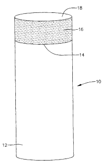
An exemplary cutting element is shown in FIG. 1. FIG. 1 shows cutting element
formed of substrate 12 and ultra hard layer 16 which is also referred to as a
cutting
table and includes top surface 18. Uttra hard layer 16 is formed of
semiconductive PCD
l0 in the present invention. Interface 14 is formed between substrate 12 and
uftra hard
layer 16. According to another exemplary embodiment, one or more transition
layers
(not shown) may be formed between uttra hard layer 16 and substrate 12. The
generally cylindrically-shaped cutting element illustrated in FIG. 1 is
intended to be
exemplary only and according to various other exemplary embodiments, the
cutting
elements and ultra-hard layers may take on any of various other shapes.
In an exemplary embodiment, the cutting element is mounted on a bit such as
the drag bit 26 shown in FIG. 2, and contacts the earthen forma.tion along
edge 28, during
driiling. In the exemplary embodiment shown in FIG. 2, the cutting elements 10
are
joined to pockets or other receiving shapes that extend into drag bit body 24
by brazing
or other means well known in the art. The illustrated arrangement is intended
to be
exemplary only and cutting elements 10 may be used in various other
arrangements in
other exemplary embodiments.
The method for forming the semiconductive PCD material includes providing a
substrate and providing a layer of diamond powder overthe substrate, then
using HTHP
processing to sinter, thereby solidifying the layer of diamond powder and
converting the
same to an ultra-hard layer of PCD, and also bonding the PCD layer to the
substrate
to form a cutting element. The substrate may be a pre-for.med solid substrate,
or it may
be provided in powder form and also solidified during the sintering operation.
The
substrate may be formed of various matrix materials. In an exemplary
embodiment, the
substrate may be formed of cemented tungsten carbide. Cemented tungsten
carbide
generally refers to tungsten carbide particles disbursed in a substrate binder
metal
matrix such as iron, nickel, or cobalt. Other substrate materials may be used
in other
exemplary embodiments. Wear resistant materials suftble for use as the
substrate
may be selected from compounds of carbide and metals selected from Groups IVB,
VB,
VIB, and VIIB of the Periodic Table of the Elements. Examples of other such
carbides
-6-
CA 02419709 2003-02-25
include tantalum carbide and titanium carbide. Substrate binder matrix
materials
suitable for use in embodiments of the invention include the transition metals
of Groups
Vi, VII, and VII of the Periodic Table of the Elements. For example, iron and
nickel are
good substrate binder matrix materials_
The layer of diamond powder used to form a semiconductive PCD material in an
exemplary embodiment of the present invention, includes of a plurality of fine
diamond
crystals. The layer of diamond powder may be provided directly on the
substrate or one
1 or more optional transition layers may be provided between the layer of
diamond
powder and the substrate.
According to one exemplary embodiment, the layer of diamond powder includes
at least some semiconductive diamond grit feedstock consisting of diamond
crystals
doped with Li, Be, or Al. The semiconductive diamond feedstock may be rnixed
with
conventional, undoped diamond feedstock to form the layer of diamond powder.
In
another exemplary embodiment, the diamond crystals of the layer of diamond
powder
may consist substantially only of semiconductive diamond grit feedstock.
According to another exemplary embodiment, the layer of diamond powder may
consist of conventional diamond crystals that are insulators such as, for
exarnple, Type
i diamond crystals. According to this exemplary embodiment, an additive such
as Li,
Be, B or Al is added to the layer of diamond powder. The additives may be in
powder
or granular form and are mixed throughout the layer of diamond powder. In an
exemplary embodiment, the additives may be mixed in uniformly throughout the
diamond powder layer. The additives are chosen to be small enough to diffuse
into the
diamond lattice formed as the layer of diamond powder solidifies to form the
PCD layer.
Because of the small size of the diamond 12ttice in PCD, the lattice can only
accommodate a limited number of impurity species (i.e., additives) for
transforming the
conventional, insulating diamond crystals to semiconductive diamond crystals_
Li, Be,
B and Al are elements that are known to be small enough to diffuse into the
diamond
lattice. Such are intended to be exemplary only and other impurity atoms or
compounds may be used in other exemplary embodiments. Li, Be, B and Al make
the
PCD a P-Type semiconductor.
The quantity of additive included in the layer of diarrtond powder ranges from
0.1
wt*/o to 10.0 wt% in an exemplary embodiment, but other weight percentages may
be
used in other exemplary embodiments. The upper limit of additive weight
percentage
-7-
CA 02419709 2003-02-25
is determined by the amount above which the sintering process is adversely
affected.
An appropriate quantity of suitably small elements or compounds of additives
are
chosen so that the additives diffuse into and throughout the diamond lattice
and cause
the insulating diamond crystals to transform to semiconductive diamond
crystals. It has
been found that a very small amount of the additives can convert the diamond
crystals
and achieve an improvement of increased conductivity. During the
transformation of
the insulating diamond materia) to a semiconductive material, some or ail of
the
diamond crystals are converted to diamond crystals having a semiconductive
surface
due to diffusion of the additive. This diffusion phenomenon takes place during
the
HTHP sintering process used to solidify the PCD, during which the additive
species are
free to diffuse throughout the PCD. It is not necessary to obtain full
conversion of the
entire diamond crystal to a semiconductive diamond crystal in order to realize
a
significant conductivity improvement_ Rather, the transformation of the
surface layer
of the diamond crystals to semiconductive surface layers, improves the
conductivity
and, hence, cuttability of the formed PCD. According to this embodiment,
undoped
diamond crystals, such as Type I diamond crystals, are converted to diamond
crystals
that include semiconductive surface layers.
According to either of the aforementioned exemplary methods of formation, an
ultra-hard material of semiconductive PCD is produced. According to either of
the
exemplary embodiments, sufficient metal binder material may be included in the
layer
of diamond powder to produce a metal binder material within the PCD material
at a
volume percentage of up to about 30%, but other volume percentages of binder
material may- be used in other exemplary embodiments. According to another
exemplary embodiment, the metal binder material may diffuse into the PCD layer
from
the substrate, during the HTHP sintering operation. In an exemplary
embodiment, the
weight percentage for metal binders may range from 8-12 /a by weight and it is
common for a weight percentage of no greater than 15% to be used_ Metals such
as
cobalt, iron, nickel, manganese, tantalum, chromium andlor mixtures or alloys
thereof
may be used as a metal binder material. The metal binder material facilitates
intercrystalline bonding between the diamond grains of the PCD layer, acts to
bond the
PCD layer to other layers or the substrate, and increases the conductivity of
the PCD
layer_ An aspect of the present invention, however, is that because of the
conductive
nature of the diamond skeleton in the semiconductive PCD formed with
semiconductive
-5-
CA 02419709 2003-02-25
diamond crystals or diamond crystals having a semiconductive surface layer, it
is not
necessary to have a metal matrix present to ensure cuttability.
According to the various embodiments of the present invention, the PCD
material
has a conductivity sufficiently high to enable cutting using EDM and EDG, even
when
the PCD was formed without a m6tal binder or after the metal matrix material
has
essentially been completely removed by leaching. In one exemplary embodiment,
PCD
of the present invention that is substantially free of metal binders, was
formed to have
1 a resistance of less than 1000 ohms. In another embodiment, the PCD layer
formed
with a metal binder therein at a weight percentage no greater than 10%, had a
resistance of less than 50 ohms.
The resistance values recited herein, are conventional resistance measurements
made using probes spaced about 1 cm apart on the sample surface.
After the solid semiconductive PCD is formed, an Electro-Discharge Machining
or Electro-Discharge Grinding cutting operation may be required to cut the PCD
to a
desired shape. Increased cutting rates can be achieved on such semiconductive
PCD
materials using EDM and EDG due to the semiconductive nature of the PCD. This
is
true even though the cooling and dielectric fluids used throughout the EDM and
EDC,
processes, and the electrical arcs produced by the EDM and EDG processes
themselves, leach any metal binder material from the semiconductive PCD during
the
cutting operation. Even if the metal binder is lost due to leaching, or if
metal binder
materials are not included at all, applicant has discovered that the PCD of
the present
invention is sufficiently conductive to ensure cuttability in Electro-
Discharge Machining
and Electro-Discharge Grinding cutting operations. The semiconductive PCD
further
includes a very high abrasion resistance while still retaining its
cuttabiiity. Since the
addition of metal binder material can be reduced or even eliminated, the
hardness,
wear resistance and thermal stability of the formed PCD layer is not
compromised and
may be improved.
After the solid semiconductive PCD is cut to form a cutting element, the
cutting
element may be joined to a drill bit body by brazing or other means well known
in the
art.
FIGS. 3-5 are graphical representations showing the advantages of exemplary
semiconductive PCD formed according to embodiments of the present invention_
FIGS.
3-5 collectively show that the semiconductive PCb formed according to the
present
-9-
CA 02419709 2003-02-25
invention includes a significantly lower resistance, i.e., a significantly
higher conductivity,
than standard PCD material. The figures also show that, after acid leaching of
the
metal matrix material during the cutting process, the semiconductive PCD of
the present
invention also exhibits a significantly reduced resistance (i.e., increased
conductivity)
with respect to standard PCD formed of conventional, insutative diamonds.
FIGS. 3-5
also show that the effect of acid leaching during the cutYing process, is
suppressed in
semiconductive PCD formed according to the present invention, in comparison to
standard PCD. "Standard PCD" consists of conventional insulative diamonds,
such as
Type I diamonds.
FIG. 3 is a Weibull plot commonly used for displaying a non-normal
distribution
of data samples and shows the measured resistance after HTHP processing of a
semiconductive PCD layer, as compared to standard PCD, as above_ Conventional
resistance measurements were made using probes spaced about 1 cm apart on the
sample surface, in all cases. In FIG. 3, Sample 1 is PCD formed by adding 2.0
weight
percent of boron to a layer of diamond powder including conventional Type I
(insulating)
diamond gritfeedstock, then sintering to convert at least some of the
insulative diamond
crystals to include a semiconductive surface layer. FIG. 3 also shows Sample 2
which
is PCD formed by adding 0_5 weight percent of boron to a layer of conventional
diamond powder including conventional Type I diamond grit feedstock, then
sintering
to convert at least some of the insulative diamond crystals to include a
semiconductive
surface layer. Each of Sample 1 and Sample 2 are PCD materials that include a
cobalt
matrix material at about 10% by weight. The standard PCD sample is a
conventional
PCD material that is substantially similar to Samples I and 2, except that the
standard
PCD material is formed only with conventional, insulative diamonds. As
illustrated in
FIG. 3, the two PCD samples of present invention exhibit a reduced resistance.
FIG. 4 is another Welbuli plot of measured electrical resistance of the PCD
material samples used in FIG_ 1, after removal of substantially all of the
cobalt matrix
phase of such samples by acid leaching. In the examples used to provide the
data
shown in FIG. 4, acid leaching was intentionally caused for data gathering
purposes,
by boiling in hydrofluoric acid and nitric acid, but other exemplary
techniques may be
used alternatively. Similar acid leaching of the cobalt matrix phase from the
PCD also
occurs as a result of the cooling and dielectric fluids used in conventional
EDM and
EDG cutting operations which can leach out any metal binder material present
in the
-10-
CA 02419709 2003-02-25
PCD material, As such, FIG. 4 is representative of PCD material during EDM and
EDG
cutting operations. FIG. 4 shows a difference of several orders of magnitude
in
resistance between each of Sample 1 and Sample 2 of the present invention, and
standard PCD. Each of the standard PCD and Samples 1 and 2 were substantially
free
of metal binder materials when the measurements plotted in FIG. 4 were made.
FIG. 5 is a bar graph summariaing the electrical resistance measurements shown
in FIGS. 3 and 4_ FIG. 5 shows that, after sintering and prior to leaching,
each of PCD
Samples 1 and 2 have a measured resistance of about 10 ohms, while the
standard
PCD sample has a measured resistance of about 400-500 ohms. In particular,
after
HTHP processing, Sample 1 has a measured resistance of about 8 ohms and Sample
2
has a measured resistance of about 20 ohms, i.e. both samples have a
resistance less
than 50 ohms. As formed, then, it can be seen that each of the semiconductive
PCD
samples exhibit a resistance of less than 10%, and more specifically less than
about
5%, of the corresponding resistance of a substantially similar PCD layerformed
only of
Type I or other conventional insulative diamonds. After leaching substantially
all metal
binder material from Samples 1 and 2 of the present invention, Samples 1 and 2
both
exhibit a measured resistance of about 1000 ohms, whereas the standard PCD has
a
resistance of about 2-3 x 101 ohms. The increase in resistance due to acid
leaching is
much more significant in the standard pCD as compared to Samples 1 and 2.
It is believed that semiconductive PCD material of the present invention
formed
using diamond grit feedstock consisting of Li-, Be- or AI-doped diamond
crystals and
without the addition of metal binder materials, will exhibit an even greater
improvement
in resistance/conductivity characteristics, than the PCD layers formed to
initially include
metal binder materials and from which the metal binder materials are
subsequently
removed by leaching (as illustrated in FIGS. 4 and 5), when compared to PCD
material
consisting only of conventional diamonds. Applicant believes that the absence
of the
additive impurity species used to convert conventional PCD to semiconductive
PCD,
provides superior diamond crystal-to-diamond crystal bonding.
Figures 3-5 and Samples I and 2 are provided to be illustrative of the
advantages of the present invention. Samples 1 and 2 are exemplary only and
the
reduced resistance advantage of the semiconductive PCD materials of the
present
invention is similarly achievable for samples formed having different metal
binder
materials and samples having binder materials present in different
percentages.
-11-
CA 02419709 2003-02-25
The semiconductive PCD material of the present invention (i.e., a PCD
layerwith
at least some Al-doped, Be-doped or Li-doped diamond crystals, or at least
some
diamond crystals having semiconductive surfaces), also has a much greater
thermal
conductivity than conventional PCD. Applicants believe that the thermal
conductivity
of the semiconductive PCD material of the present invention may be 15 times
greater
than the conductivity of conventional PCD material at 80 i6 and 4-5 times
greater than
the conductivity of conventional PCD material at room temperature_ When used
as a
cutting layer in a cutting tool, a semiconductive PCD material is better able
to conduct
the heat generated by the abrasion of the PCD cutting layer against the object
being
cut, and thus maintain a lower temperature on the cutting layer. Increased
temperatures on the cutting layer and the tool are known to decrease the life
of the
cutting tool_ Consequently, the use of the semiconductive PCD of the present
invention
as a cuiting layer, will provide an increased operating life of the cutting
element.
The preceding merely illustrates the principles of the invention. It will thus
be
appreciated that those skilled in the art will be able to devise various
arrangements
which, although not explicitly described or shown herein, embody the
principles of the
invention and are included within the scope and spirit. Furthermore, all
examples and
conditiohal language recited herein are principally intended expressly to be
only for
pedagogical purposes and to aid in understanding the principles of the
invention and
the concepts contributed by the inventors to furthering the art, and are to be
construed
as being without limitation to such specifically recited examples and
conditions.
Moreover, all statements herein reciting principles, aspects, and embodiments
of the
invention, as well as specific examples thereof, are intended to encompass
both
structural and the functional equivalents thereof. Additionally, it is
intended that such
equivalents include both currently known equivalents and equivalents developed
in the
future, i.e., any elements developed that perform the same function,
regardless of
structure. The scope of the present invention, therefore, is not intended to
be limited
to the exemplary embodiments shown and described herein. Rather, the scope and
spirit of the present invention is embodied by the appended claims.
-12-