Note: Descriptions are shown in the official language in which they were submitted.
CA 02419940 2003-02-25
WO 02/21459 PCT/USO1/27293
METHOD OF COIN DETECTION AND BAG STOPPING FOR A COIN SORTER
TECHNICAL FIELD
The invention relates to coin processing equipment and,
more particularly, to coin sorters.
BACKGROUND ART
Coin sorters are used to sort and collect coins by
denomination, such as penny, nickel, dime, quarter, half and
dollar in the United States. Other denominations may be
handled in countries outside the United States. In coin
sorters, it has been the practice to attach bags or coin
receptacles to collect the coins for respective denominations.
As used herein the term "bags" shall be understood to include
all types of removable receptacles used to collect coins by
denomination. The bags are sued and defined to hold a
certain number of coins, such as 5000 pennies or 2000
quarters. This number or limit on coins in a bag is referred
to in the technical field as a "bag stop".
As the coins are being sorted, there is the problem of
one of the bags becoming filled to the limit, at which time
either the machine has to be stopped, or another bag switched
into place to receive more coins of that denomination.
One method of counting coins and stopping the coin sorter
based on bag limit counts is disclosed in Jones et al., U.S.
Pat. Nos. 5,514,034; 5,474,497 and 5,564,978. In these
patents, the coin sensors are placed outside the exit channels
for counting the coins after they are sorted.
Other methods for sensing and counting coins for bag
stopping are provided in Ma~ur et al., U.S. Pat. Nos.
5,299,977; 5,429,550; 5,453,047 and 5,480,348. In the Mazur
'977 patent, the sensors for totaling coin counts are located
in each exit channel, so that the coins are effectively sorted
before they are counted. In the Mazur '550 patent, one of the
- 1 -
CA 02419940 2003-02-25
WO 02/21459 PCT/USO1/27293
sorting methods involves sensing the coins upstream of the
sorting exits and monitoring the angular movement of the disk
using an encoder. In the Mazur '550 patent, mechanical contact
sensors are disclosed as being positioned at a certain
position relative to the width of a coin to detect the leading
and trailing edges of a single denomination, or of less than
all denominations, by physically contacting the coin. In one
example, a single contact sensor is used in conjunction with
an encoder which tracks angular movement of the disc to
calculate a chord length of each coin to detect the
denomination.
In the prior art such as Mazur '550 patent, there has been
a pre-warn sensing of the fifth last coin, and then a motor
stopping sequence involving, a first stop, a slow speed jog
and a final stop. As used herein the term "exact bag stop"
means a bag stopping action which would cause the last coin
for a denomination to be collected in a bag (or other
receptacle).
The present invention is designed to provide a novel and
improved approach for detecting coins and bag stopping,
including stopping at exact bag stops. The invention is
disclosed as an enhancement to a sorter of the type shown and
described in Zwieg et al., U.S. Pat. No. 5,992,602 and offered
commercially under the trade designation, "Mach 12," by the
assignee of the present invention.
In this prior coin sorter, coins were identified by using
an inductive sensor to take three readings as each coin passed
through a coin detection station and these readings were
compared against prior calibrated readings for the respective
denominations.
Optical sensing of coins in coin handling equipment has
been employed in Zimmermann, U.S. Pat. No. 4,088,144 and
Meyer, U.S. Pat. No. 4,249,648. Zimmermann discloses a rail
sorter with a linear photosensing array. Zimmermann does not
disclose repeated scanning of the coin as it passes the array,
but suggests that there may have been a single detection of
- 2 -
CA 02419940 2003-02-25
WO 02/21459 PCT/USO1/27293
the widest part of the coin. Zimmermann also does not disclose
any processing of coin sensor signals. In response to
detection of a number of coins, Zimmermann operates an
electromagnet to clamp down on a coin on a belt to stop
movement of the coins. Zimmermann does not disclose any
manner of braking a motor or conveying the last coin to a coin
bag or receptacle.
Meyer, U.S. Pat. No. 4,249,648, discloses optical imaging
of coins in a bus token collection box. Meyer does not fully
describe, however, the resulting operations after a limit
number of a coin denomination is reached.
SUMMARY OF THE INVENTION
The invention relates to a method and apparatus for
utilizing an optical detector to rapidly count coins before
they are sorted, and upon reaching a bag stop limit, either
reducing speed or stopping a motor that causes movement of the
coins in a coin sorting machine.
The method includes optically measuring at least a
portion of each coin at a location upstream from sorting
openings for sorting the coins and generating dimensional data
for each respective coin; using the coin dimensional data for
counting the coins by denomination for bag stopping purposes
before said coins are sorted and counted for totalizing
purposes; limiting further movement of the coins when the
optical measuring produces data indicative of a bag stop limit
being reached for a respective denomination; and detecting a
last coin as it moves through a respective sorting opening.
The invention is applied in one preferred embodiment to a
coin sorting machine having a coin sorting member with a
plurality of sorting openings by which respective
denominations of coins are sorted, having a coin driving
member for moving the coins to the coin sorting openings,
having a motor coupled to the coin driving member, and having
a brake for stopping the motor.
- 3 -
CA 02419940 2003-02-25
WO 02/21459 PCT/USO1/27293
The invention further provides a controller for receiving
coin size data and counting each coin for bag stopping
purposes separate from the counts maintained for totalizing
the sorted coins. A main controller stores bag stop limits.
When a bag stop limit is reached for a respective
denomination, the main controller then transmits signals to.
stop, or reduce the speed of, the motor driving the coin
sorting assembly.
The present invention is also capable of providing exact
bag stop limits, where the machine is stopped or slowed down
as the last coin in a bag is sorted into the bag.
In a further aspect of the invention, the coin sorting
machine is stopped if the bag stop limit is reached for the
denomination with a sorting aperture closest to the sensor.
If the bag stop limit is reached for a denomination with a
sorting aperture further along the sorting path, then the
machine can reduce speed and then stop, or stop and be moved
slowly (jogged) until the coin drops through the appropriate
sorting aperture, where it is detected by the conventional
coin count sensors.
One object of the present invention is to use an optical
imaging system in place of the prior art mechanical sensors.
Another object of the invention is to provide a sorter
for coin detection and bag stopping that does not utilize an
encoder for tracking coins.
Another object of the present invention is to provide an
enhanced type of contactless coin sensor assembly for both
coin counting for bag stopping and detection of invalid coins
for offsorting.
While the present invention is disclosed in a preferred
embodiment based on Zwieg et al., U.S. Pat. No. 5,992,602, the
invention could also be applied as a modification to other
types of machines, including the other prior art described
above.
The invention provides exact bag stopping for a high
speed coin sorter.
- 4 -
CA 02419940 2003-02-25
WO 02/21459 PCT/USO1/27293
Other objects and advantages of the invention, besides
those discussed above, will be apparent to those of ordinary
skill in the art from the description of the preferred
embodiments which follow. In the description, reference is
made to the accompanying drawings, which form a part hereof,
and which illustrate examples of the invention. Such
examples, however, are not exhaustive of the various
embodiments of the invention, and therefore, reference is made
to the claims which follow the description for determining the
scope of the invention.
BRIEF DESCRIPTION OF THE DRAWINGS
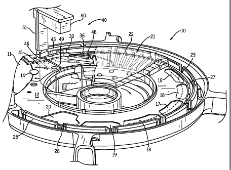
Fig. 1 is a perspective view of a portion of the coin
sorter incorporating the present invention;
Fig. 2 is top plan view of a sorter plate in the coin
sorter of Fig. 1;
Fig. 3 in an exploded detail view of the optical sensor
assembly in the coin sorter of Fig. 1;
Fig. 4 is a side view in elevation of a bottom portion of
the coin sorter of Fig. 1 showing a motor and a brake;
Fig. 5A is sectional view in elevation of the brake seen
in Fig. 4;
Fig. 5B is a detail sectional view taken in plane
indicated by line 5B-5B in Fig. 5C;
Fig. 5C is a detail sectional view taken in plane
indicated by line 5C-5C in Fig. 5A;
Fig. 6A is a block diagram of the sensor circuit module
seen in Fig. 3;
Figs. 6B and 6C are enlarged detail diagrams of a coin
passing through the sensor assembly of Fig. 3; and
Fig. 6D is a timing diagram of the operation of the
sensor circuit module of Fig. 6A;
Fig. 7 is a schematic of the overall electrical control
system of the sorter of Fig. 1;
Fig. 8 is a flow chart of operation of the main
- 5 -
CA 02419940 2003-02-25
WO 02/21459 PCT/USO1/27293
controller of Fig. 7.
DETAILED DESCRIPTION OF THE PREFERRED EMBODIMENTS
Referring to Fig. 1, the coin handling machine 10 is a
sorter of the type shown and described in Zwieg et al., U.S.
Pat. No. 5,992,602, and offered under the trade designation,
"Mach 12" by the assignee of the present invention. This type
of sorter 10, sometimes referred to as a figure-8 type sorter,
has two interrelated rotating disks, a first disk operating as
a queueing disk 11 to separate the coins from an initial mass
of coins and arrange them in a single file of coins 14 to be
fed to a sorting disk assembly. The sorting disk assembly has
a lower sorter plate 12 with coin sensor station 40, an
offsort opening 31 (see Fig. 2) and a plurality of sorting
apertures 15, 16, 17, 18, 19 and 20. There may be as many as
ten sorting apertures, but only six are illustrated for this
embodiment. The first five sorting apertures are provided for
handling U.S. denominations of penny, nickel, dime, quarter
and dollar. The sixth sorting opening can be arranged to
handle half dollar coins or used to offsort all coins not
sorted through the first five apertures.
As used herein, the term "apertures" shall refer to the
specific sorting openings shown in the drawings. The term
sorting opening shall be understood to not only include the
apertures, but also sorting grooves, channels and exits seen
in the prior art.
The sorting disk assembly also includes an upper,
rotatable, coin driving member 21 with a plurality of webs 22
or fingers which push the coins along a coin sorting path 23
over the sorting apertures 15, 16, 17, 18, 19 and 20. The coin
driving member is a disk, which along with the webs 22, is
made of a light transmissive material, such as acrylic. The
webs 22 are described in more detail in Adams et al . , U. S .
Pat. No. 5,525, 104, issued June 11, 1996. Briefly, they are
aligned along radii of the coin driving member 21, and have a
- 6 -
CA 02419940 2003-02-25
WO 02/21459 PCT/USO1/27293
length equal to about the last 30% of the radius from the
center of the circular coin driving member 21.
A rail formed by a thin, flexible strip of metal (not
shown) is installed in slots 27 to act as a reference edge
against which the coins are aligned in a single file for
movement along the coin sorting path 23. As the coins are
moved clockwise along the coin sorting path 23 by the webs or
fingers 22, the coins drop through the sorting apertures 15,
16, 17, 18, 19 and 20. according to size, with the smallest
size coin dropping through the first aperture 15. As they
drop through the sorting apertures, the coins are sensed by
photo emitters in the form of light emitting diodes (LEDs)
15a, 16a, 17a, 18a, 19a and 20a (Fig. 2) and optical detectors
15b, 16b, 17b, 18b, 19b and 20b (Fig. 2) in the form of
phototransistors, one emitter and detector per aperture. The
photo emitters 15a, 16a, 17a, 18a, 19a and 20a are mounted
outside the barriers 25 seen in Fig. 1 and are aimed to
transmit a beam through spaces 26 between the barriers 25 and
an angle from a radius of the sorting plate 21, so as to
direct a beam from one corner of each aperture 15, 16, 17, 18,
19 and 20 to an opposite corner where the optical detectors
15b, 16b, 17b, 18b, 19b and 20b (Fig. 2) are positioned.
As coins come into the sorting disk assembly 11, they
first pass a coin sensor station 40 (Fig. 1). In the prior
art, this station 40 was used to detect coin denominations
using an inductive sensor, as well as to detect invalid coins.
Invalid coins were then off-sorted through an offsort opening
31 with the assistance of a solenoid-driven coin ejector
mechanism 32 (Figs. 1, 2 and 7) having a shaft, which when
rotated, directs a coin to an offsort edge 36 and ultimately
to offsort opening 31. This offsorting of coins occurs in the
same place, however, the present embodiment utilizes a
different type of coin validity sensing at coin sensor station
40.
The coin sensor station includes a coin path insert 41.
This coin path insert 41 is preferably made of a nonmagnetic
_ 7 _
CA 02419940 2003-02-25
WO 02/21459 PCT/USO1/27293
material, for example, a zirconia ceramic, so as not to
interfere with inductive sensors to be described. Two
inductive sensors 42, 43 (shown in phantom in Figs. 1 and 2)
are inserted from the bottom of the coin path insert 41. One
sensor 42 is for sensing the alloy content of the core of the
coin, and another sensor 43 is for sensing the alloy content
of the surface of the coin. This is especially useful for
U.S, coins of bimetal clad construction. The two inductive
sensors 42, 43 are inserted on opposite sides of a radially
aligned slit 44, which is used for the optical image detector
to be described. The slit 44 is preferably filled or covered
by a light transmissive, sapphire window element 49.
The coin path insert 41 also has a curved outside rail 45
for guiding the coins. A thickness and edge alloy inductive
sensor 46 is embedded in this rail 45 so as not to project
into the coin sorting path 23. The operation of the sensors
42, 43 and 46 relates to detection of invalid coins for
offsorting.
The coin path insert 41 has a curved edge 47 on one end
for interf acing with the queueing disk, and a sloping surf ace
48 at an opposite end leading to the offsort opening 31.
A housing shroud 50 (Fig. 1) is positioned over the
window element 49, and this shroud 50 contains an optical
source provide by a staggered array of light emitting diodes
(LED's) 54 (Fig. 6A) for beaming down on the coin path insert
41 and illuminating the edges of the coins 14 as they pass by
(the coins themselves block the optical waves from passing
through). The optical waves generated by the light source may
be in the visible spectrum or outside the visible spectrum,
such as in the infrared spectrum. In any event, the terms
"light" and "optical waves" shall be understood to cover both
visible and invisible optical waves.
The housing cover 50 is supported by an upright post
member 51 of rectangular cross section. The post member 51 is
positioned just outside the coin sorting path 23, so as to
allow the elongated optical source 54 to extend across the
_ g _
CA 02419940 2003-02-25
WO 02/21459 PCT/USO1/27293
coin sorting path 23 and to be positioned directly above the
elongated slit 44.
Underneath the coin path insert 41 is a housing 52 (Fig.
1) of aluminum material for containing a coin sensing module
53 (Fig. 3). As used herein, the term "circuit module" shall
refer to the combination of circuit packages and the
electronic circuit board upon which the circuit packages are
mounted to form an electronic circuit. As seen in Fig. 3, the
housing 52 has a body, with a body cavity, and a cover (which
has been removed) enclosing the body cavity.
The circuit module 53 supports a linear array 55 of
photodetector diodes, such that when the circuit module 53 is
positioned properly in the housing 52 (Fig. 3) (the shape of
the circuit module 53 is keyed to the shape of the housing
52), the linear array 55 will be positioned below the window
49. A linear lens array 56 is disposed between the window 49
and the photodiode array 55 to beam the light from the slit 49
to the photodiode array 55, and also to diffuse concentrations
of light from the LEDs 54.
Figs. 4 and 5 show a DC electric motor 60 for driving the
two moving disks in the coin sorter 10. The motor 60 is
connected through a belt 61 to a rotatable transfer shaft 59
with one pulley 62 being driven by belt 61 and a second pulley
63 for transferring power to a second belt 64 directly driving
coin driving member 21 and the driving member 11 in the
queueing portion of the machine 10. An electromechanical
brake 65 is mounted to the bottom of the motor 60. The brake
65 is used for bag stops and emergency stops, while dynamic or
regenerative braking is used for all types of stops.
Referring next to Fig. 5A, the brake 65 has a coil 66
which is bolted to a lower end of the motor 60 and receives an
electrical "brake on" signal for braking. A collar 68 is
fastened by a bolt to a lower end of a motor output shaft 67.
The collar 68 is connected to brake shoe 69 by leaf springs
70 and screws 71, which allows controlled separation of the
collar 68 and brake shoe 69 in a direction parallel to the
- 9 -
CA 02419940 2003-02-25
WO 02/21459 PCT/USO1/27293
axis of rotation for the motor shaft 67. When a braking
signal is sent to coil 66, it will cause frictional braking of
the motor 60.
Fig. 6A shows the details of a sensor circuit module 53
including five (5) sub-modules 80, 81, 82, 83 and 84 each
utilizing an embedded microcontroller.
A core alloy detector sub-module 80 utilizes a 9.3 mm
sensing coil 86 embedded in the sensor 42 and coupled to an
oscillator 87 operating at 180 kHz. As a coin enters the
field of the coil (see Fig. 6A), the oscillator impedance is
altered by the eddy currents developed in the coin, resulting
in both frequency and voltage changes. The frequency is
measured by a phase locked loop (PLL) circuit 88 acting as a
frequency to voltage converter. The phase locked loop circuit
88 acts to respond very quickly to frequency changes. The
voltage of the oscillator is measured by rectifying the sine
wave through rectifier circuit 89 and reading it with an
analog to digital (A/D) converter integrated with a
microcontroller 90. The microcontroller is preferably a PIC
16C715 microcontroller available from Microchip Technology,
Inc., Chandler, Arizona, USA. The reading of the coin alloy
data occurs when the coin fully covers the sensor coil 86 as
determined by a diameter sensor trigger point 57, illustrated
in Fig. 6B. Therefore, the reading is taken relative to a
specific position in the coin path 23. Values for the voltage
and frequency are transferred to the coin sensor module
interface controller 84.
A thickness/edge alloy detector sub-module 81 (Fig. 6A)
provides a single data output as a function of both coin
thickness and alloy composition. A 3.3 mm sensing coil 91 is
mounted in sensor 46 in the side rail 45 (Fig. 1) along the
coin path 23 with the active field perpendicular to the core
alloy detector 42. The sensor coil 91 (Fig. 6A) oscillates at
640 kHz as provided by oscillator 92. As a coin to be tested
approaches (Fig. 6B), the presence of the coin material
changes the impedance of the oscillator 92. The output of the
- 10 -
CA 02419940 2003-02-25
WO 02/21459 PCT/USO1/27293
oscillator 92 is rectified by a diode rectifier circuit 93 and
sampled many times by an analog-to-digital converter
integrated into a second microcontroller 94, which may be of
the same type as microcontroller 90. When the maximum
influence (lowest output) of a coin is determined, the value
is transmitted to coin sensor module interface controller 84.
An optical coin size sensor module 82 forms a closed loop
system controlled by a microcontroller 95, similar to
microcontrollers 90 and 94. The illumination source,
comprised of multiple LED's 54 in a staggered pattern (Fig.
6A), illuminates the coin sensing area with light energy which
in turn is detected by the photodiode array 55, which provides
a 1x768 pixel array below the coin path insert 41. A krypton
bulb (not shown) may be included in the illumination source to
assure enough emission of light waves in the infrared range.
The light waves are emitted through the light transmissive
drive member 21, and the sapphire window 49 flush with the
coin path insert 41. A dual comparator method is used to
differentiate between the gradual transition of webs 22 on the
drive member 21 and the abrupt transition of the coin edge.
This method is carried out in FPGA 97.
When the shadow of a coin 14 covers at least a portion of
the linear detection array 55, readings will taken between a
first light-to-dark transition 57a and a first dark-to-light
transition 57b as seen in Fig. 6B. Additional readings will
be taken between a second light-to-dark transition 58a and a
second dark-to-light transition 58b as seen in Fig. 6C. The
readings are repeated each 400 microseconds between readings
in Figs. 6B and 6C to get the most samples possible. The
value halfway between each pair of points 57a, 57b and 58a,
58b, is the radius. A radius is calculated each 400
microseconds. An average radius is calculated by the
processor 95 and transmitted to processor 96.
The resulting coin size data are transferred to the
sensor module interface controller 84. The multiple samples
minimize the effect of nicked or non-round edges.
- 11 -
CA 02419940 2003-02-25
WO 02/21459 PCT/USO1/27293
The microcontroller CPU 95 reads imaging data from a
field programmable gate array (FPGA) 97, which connects to the
(number of elements) photodiode array 55 through the CPU 96.
The FPGA 97 receives and interprets pixel imaging signals from
the photodiode array 55 which are then read by the
microcontroller CPU 95, and used to calculate the radius of
each coin as it passes the window 49. The photodiode array 55
does not necessarily span the full diameter of each coin, and
an offset may be used to calculate the full diameter. While
radius data is used in this embodiment, it should be apparent
that diameter data is an equivalent that could also be used
when the radius is multiplied by two. The term "dimensional
data" or "coin size" data shall include radius data, diameter
data and other data from which coin size can be derived. The
coin size data is then communicated to the second
microcontroller CPU 96.
A surface alloy detector sub-module 83 includes a 9.3 mm
sensing coil 99, which oscillates at a nominal frequency of
lMHz as provided by oscillator 100. Two phase locked loop
devices 104, 105 are used, one to reduce the frequency, the
other to measure the frequency. A summing circuit 103 and a
fourth order filter 102 are used in one of the loops. A
voltage representing a magnitude of the sensed signal is
obtained by rectifying the sine wave with diode rectifier
circuit 106 and reading the result with an analog-to-digital
converter included in a microcontroller 107. This
microcontroller is a PIC 16C72 microcontroller available from
Microchip Technology, Inc., of Chandler, Arizona, USA. The
reading of the coin alloy data occurs when the coin fully
covers the sensor 43 and sensor coil 99 as determined by the
sensor trigger point 57 (Fig. 6C). Therefore, the reading is
taken relative to a specific position in the coin path 23.
Values for the voltage and frequency are then transferred to
an interface controller module 84 for the sensor module 53.
The interface controller module 84, includes a
microcontroller CPU 96 for reading the core voltage, core
- 12 -
CA 02419940 2003-02-25
WO 02/21459 PCT/USO1/27293
frequency, thickness, coin size, surface voltage and surface
frequency data from the other detector modules 80, 81, 82 and
83 and transmitting the data to the coin offsort controller
module 110 in Fig. 7. The interface controller 96 is
preferably a PIC 16C72 microcontroller circuit available from
Microchip Technology, Inc., of Chandler, Arizona, USA. Other
suitable CPU microcontrollers may be used for the
microcontrollers described above in the sub-modules 80-84.
The interface microcontroller CPU 96 connects to a coin
offsort controller module 110 (Fig. 7) through an interrupt
request line (IRQ), a three-bit address bus, an eight-bit data
bus and a set of line drivers 98.
The manner in which the interface controller 96 reads
data from the sub-modules 80, 81, 82 and 83 is illustrated in
the timing diagram of Fig. 6D. First, the data for magnitude
and frequency from the core alloy sensor 42 is read into sub-
module 80 in 15-microsecond intervals 111, 112 beginning at
trigger point 57 in Figs. 6B and 6C (T1 in Fig. 6D). Then,
the data from the core alloy sensor 42 is read by the
interface controller 96 in 30-microsecond intervals 113, 114,
separated by a 20-microsecond interval. Next, the data from
this edge alloy thickness sensor 46 is read into sub-module 81
in interval 115, and then the coin passes over the imaging
sensor 54, 55, such that size readings are read by sub-module
82 and the coin size is calculated in time frame 116. The
interface controller 96 then reads in the data for data
thickness and coin size in time frames 117, 118. The order of
these two qualities, coin edge data and coin size data, could
be reversed between themselves, but would still follow the
core alloy sensing data. Lastly, as the coin passes the
surface alloy sensor and the trigger point 57 in Figs. 6B and
6C (T2 in Fig. 6D), sub-module 83 reads in data in 15-
microsecond intervals 126, 127 and the interface controller
reads the surface alloy data for magnitude and frequency in
30-microsecond intervals 128, 129, separated by a 20-
microsecond interval.
- 13 -
CA 02419940 2003-02-25
WO 02/21459 PCT/USO1/27293
In one embodiment of the present invention, the sensors
42, 43 and 46 for checking validity of coins for offsorting
purposes are not used. Only the photodiode array 55 for
detecting a size dimension of each coin is used for sensing
coins passing the coin path insert 41. In this simplified
embodiment, a coin offsort controller module 110 (Fig. 7) is
not necessary, and the data from the coin sensor module 53 is
transmitted directly to a main machine controller CPU module
120 seen in Fig. 7 through a three-bit address bus and an
eight-bit data bus and a set of line drivers, designated as
Port 2. In the embodiment in which the sensors 42, 43 and 46
are used in the sensor module 53, the coin sensor module 53
communicates through Port 1 (P1) and a feed-through connection
on the main controller CPU 120 (J10-J11 connecting to P10-P11
on the coin offsort controller module).
Referring to Fig. 7, the machine controller CPU 120 has
six I/O ports (STA 1 - STA 6) for sending output signals to
the light emitting diodes 15a, 16a, 17a, 18a, 19a and 20a and
receiving signals from the optical detectors 15b, 16b, 17b,
18b, 19b and 20b for the six sorting apertures. The main
controller CPU 120 thereby detects when coins fall through
each sorting aperture 15-20 and can maintain a count of these
coins for totalizing purposes. By "totalizing" is meant the
counting of coin quantities and monetary value for purposes of
informing a user through a display, such as LED readout
display 122, which is interfaced with a keyboard through
interface 123 to the main controller CPU 120.
The main controller CPU 120 is interfaced through
electronic circuits to control the DC drive motor 60. In
particular, the main controller CPU 120 is connected to
operate a relay 125 which provides an input to an electronic
motor drive circuit 124. This circuit 124 is of a type known
in the art for providing power electronics for controlling the
DC motor 60. This circuit 124 receives AC line power from a
power supply circuit 121. The motor drive circuit 124 is also
connected to a dynamic braking resistor R1 to provide dynamic
- 14 -
CA 02419940 2003-02-25
WO 02/21459 PCT/USO1/27293
electrical motor braking for the DC motor 60.
The coin offsort controller module 110 includes a
microelectronic CPU, such as a Philips P51XA, as well as the
typical read only memory, RAM memory, address decoding
circuitry and communication interface circuitry to communicate
with the sensor control module 53 and the main controller CPU
120 as shown in Fig. 7. The coin offsort controller module
110 is connected to operate the coin ejector mechanism 32,
when an invalid coin is sensed at coin sensing station 40.
Referring next to Fig. 8, the operation of the main
controller CPU module 120 in braking the coin driving member
21 in response to reaching a bag stop limit is charted. This
start of this portion of the program of the respective CPU 120
is represented by the start block 130. The coin sensor module
53 indicates the detection of the leading edge of a next coin,
thereby signaling to the main controller CPU 120 that coin
size data for the preceding coin is now ready for upload,
along with five bytes of data concerning coin validity,
including a thickness byte resulting from signals from
thickness sensor 46 and frequency and magnitude bytes
resulting from signals from each of the alloy sensors 42, 43.
The data is the uploaded as represented by process block 132.
The main controller CPU 120 processes this data to
determine if the coin should be rejected, as represented by
decision block 133. If the answer is "YES" as represented by
the "YES" branch from decision block 133, the program returns
to block 131 to process the next coin. If the answer is "NO"
as represented by the "NO" branch from decision block 133, the
coin is added to the count for the respective denomination and
compared to the count for a bag stop limit number, as
represented by process block 134. If a bag stop is determined,
as represented by the "YES" result from decision block 134, the
main controller CPU 120 executes program instructions to
determine if this is the "smallest" denomination representing
the closest sorting aperture. It should be appreciated here
that if the sorting openings were other than apertures in a
- 15 -
CA 02419940 2003-02-25
WO 02/21459 PCT/USO1/27293
flat surface, then the order of denominations might be
reversed with the largest coin being sorted first. In any
event, it is the sorting aperture closest to the coin sensor
station 40 that provides the shortest stopping distance.
If this answer is "YES" as a result of executing the
decision in decision block 135, then the main controller CPU
120 transmits a signal to apply the brake 65 to stop the motor
60 in the shortest time and corresponding distance of movement
of the coin driving member 21 as represented by process block
136. Next, as represented by decision block 137, the main
controller CPU executes program instructions to determine if
the coin was detected as it passed one of the optical
detectors 15b, 16b, 17b, 18b, 19b or 20b. When this has
occurred, the last coin has been sorted and presumably passed
to the bag or receptacle to provide the exact bag stop. If in
executing decision block 137, the result is "N0," then the main
controller CPU 120 issues a command (process block 138) to
move the motor forward at low speed ("jog") the motor 60, and
then executes program instructions represented by decision
block 137 to see if the coin has been sorted into the bag. At
that time the motor 60 is stopped, and the operator is
signaled through a visual or audible alarm, or both, to
replace the filled bag with an empty bag and restart the
machine 10, as represented by process block 143. The CPU 120
then loops back to re-execute the steps seen in Fig. 8 for the
next coin.
In the event that the answer in decision block 135 is
"NO," meaning the denomination does not correspond to the
sorting aperture 15 closest to the sensing station 40, the
main controller CPU 120 transmits a signal to the motor
control circuit 124 to slow the motor by dynamic electrical
braking through resistor R1 to a predetermined slower speed
than full operating speed, and this is represented by process
block 140 in Fig. 8. The CPU 120 then executes program
instructions, as represented by decision block 141, to
determine if the coin was detected as it passed one of the
- 16 -
CA 02419940 2003-02-25
WO 02/21459 PCT/USO1/27293
optical detectors 15b, 16b, 17b, 18b, 19b or 20b. Tf the
answer is "NO" it loops back to process block 140 to further
reduce motor speed and then re-executes decision block 141.
When the coin is detected, as represented by the "YES" result,
the CPU 120 transmits signals through motor control circuit
L24 to operate the brake 65 to brake the motar 60, as
represented by process block 142. At that time the motor 60
is stopped, and the operator is signaled through a visual or
audible alarm or both to replace the filled bag with an empty
bag and restart the machine 10, as represented by block 143.
This completes the description of a method and apparatus
for utilizing optical imaging to rapidly count coins before
they are sorted, and upon reaching a bag stop limit, either
reducing speed or stopping a motor that causes movement of the
coins in a coin sorting machine.
This has been a description of the preferred embodiments
of the method arid apparatus of the present invention. Those
of ordinary skill in this art will recognize that still other
modifications might be made while still coming within the
spirit and scope of the invention and, therefore, to define
the embodiments of the invention, the following claims are
made.
- 17 -