Note: Descriptions are shown in the official language in which they were submitted.
CA 02421934 2003-03-11
WO 02/22492 PCT/USO1/28608
MICROELECTROMECHANICAL FLEXIBLE
MEMBRANE ELECTROSTATIC VALVE DEVICE AND RELATED
FABRICATION METHODS
FIELD OF THE INVENTION
The present invention relates to microelectromechanical system (MEMS)
valve structures, and more particularly to low-powex, high speed
electrostatically
actuating MEMS valve structures and the associated fabrication methods.
BACKGROUND OF THE INVENTION
Advances in thin film technology have enabled the development of
sophisticated integrated circuits. This advanced semiconductor technology has
also been leveraged to create MEMS (Micro Electro Mechanical System)
structures. MEMS structures are typically capable of motion or applying force.
Many different varieties of MEMS devices have been created, including
microsensors, microgears, micromotors, and other microengineered devices.
MEMS devices are being developed for a wide variety of applications because
they
provide the advantages of low cost, high reliability and extremely small size.
Design freedom afforded to engineers of MEMS devices has led to the
development of various techniques and structures for providing the force
necessary
to cause the desired motion within microstructures. For example,
microcantilevers
have been used to apply rotational mechanical force to rotate micromachined
springs and gears. Electromagnetic fields have been used to drive micromotors.
Piezoelectric forces have also been successfully been used to controllably
move
micromachined structures. Controlled thermal expansion of actuators or other
MEMS components has been used to create forces for driving microdevices. One
such device is found in United States Patent No. 5,475,318 entitled
"Microprobe"
issued December 12, 1995 in the name of inventors Marcus et al., which
leverages
CA 02421934 2003-03-11
WO 02/22492 PCT/USO1/28608
issued December 12, 1995 in the name of inventors Marcus et al., which
leverages
thermal expansion to move a microdevice. A micro cantilever is constructed
from
materials having different thermal coe~cients of expansion. When heated, the
bimorph layers arch differently, causing the micro cantilever to move
accordingly.
A similar mechanism is used to activate a micrornachined thermal switch as
described in United States Patent No. 5,463,233 entitled "Micromachined
Thermal
Switch" issued October 31, 1995 in the name of inventor Norling.
Electrostatic forces have also been used to move structures. Traditional
electrostatic devices were constructed from laminated films cut from plastic
or
mylar materials. A flexible electrode was attached to the film, and another
electrode was affixed to a base structure. Electrically energizing the
respective
electrodes created an electrostatic force attracting the electrodes to each
other or
repelling them from each other. A representative example of these devices is
found
in United States Patent No. 4,266,339 entitled "Method for Making Rolling
Electrode for Electrostatic Device" issued May 12, 1981 in the name of
inventor
Malt. These devices work well for typical motive applications, but these
devices
cannot be constructed in dimensions suitable for miniaturized integrated
circuits,
biomedical applications, or MEMS structures.
MEMS electrostatic devices are used advantageously in various
applications because of their extremely small size. Electrostatic forces due
to the
electric field between electrical charges can generate relatively large forces
given
the small electrode separations inherent in MEMS devices. An example of these
devices can be found in United States Patent Application No. 09/345,300
entitled
"ARC resistant High Voltage Micromachined Electrostatic Switch" filed on June
30, 1999 in the name of inventor Goodwin-Johansson and Untied States Patent
Application No. 091320,891 entitled "Micromachined Electrostatic Actuator with
Air Gap" filed on May 27, 1999 in the name of inventor Goodwin-Johansson.
Both of these applications are assigned to MCNC, the assignee of the present
invention.
Typical MEMS valves have employed thermal actuation/activation
methods to control valves with high flow rates (i.e. large apertures and large
clearance areas around the aperture). Thermal actuation has been preferred
-2-
CA 02421934 2003-03-11
WO 02/22492 PCT/USO1/28608
because it is able to provide the large forces necessary to control the valve
over the
requisite large distances. However, these valves have relatively slow
operation
rates due to the thermal time constraints related to the valve materials.
Additionally, thermally activated MEMS valves use resistive heating where the
power consumed is calculated by the current squared times the resistance and
considerable power is consumed in operating the valve.
It would be advantageous to construct a MEMS valve device using
electrostatic actuation that is capable of both large displacements and large
forces.
The electrostatic nature of the MEMS valve will allow for relatively low power
consumption and, therefore, no unwarranted heating of the flowing gas or fluid
would occur. Additionally, the electrostatic valve will provide for relatively
fast
operation, allowing for more precise control of the open and closed states of
the
valve. In addition, it would be advantageous to develop a MEMS valve that
forms
a secure valve seat to valve cover interface to assure low leakage rates are
realized.
It would also be beneficial to provide for a MEMS valve that minimizes the
occurrence of stiction between the substrate and moveable membrane. Suction,
which is a well-known concept in microelectronics, is defined as the tendency
for
contacting MEMS surfaces to stick to one another. Stiction is especially a
concern
in valve devices in which a pressure differential exists across the closed
valve. It
would be beneficial to devise a MEMS valve that relieves the pressure
differential
prior to opening the valve.
As such, MEMS electrostatic valves that have improved performance
characteristics are desired for many applications. For example, micromachined
valves capable of fast actuation, large valve force and large valve flap
displacements that utilize minimal power are desirable, but are currently
unavailable.
SUMMARY OF THE INVENTION
The present invention provides for improved MEMS electrostatic valves
that benefit from large valve force, fast actuation and large displacement of
the
moveable membrane to allow for the efficient transport of increased amounts of
gas or liquid through the valve. Further, methods for making the MEMS
electrostatic valve according to the present invention are provided.
-3-
CA 02421934 2003-03-11
WO 02/22492 PCT/USO1/28608
A MEMS valve device driven by electrostatic forces according to the
present invention comprises a planar substrate having an aperture formed
therein
and substrate electrode disposed on the planar substrate. Further, the MEMS
valve
device of the present invention includes a moveable membrane that overlies the
S aperture and has an electrode element and a biasing element. The moveable
membrane is defined horizontally as having a fixed portion attached to the
substrate and a distal portion that is moveable with respect the substrate.
Additionally, at least one resiliently compressible dielectric layer is
provided to
insure electrical isolation between the substrate electrode and electrode
element of
the moveable membrane. In operation, a voltage differential is established
between the substrate electrode and the electrode element of the moveable
membrane to move the membrane relative to the aperture to thereby controllably
adjust the portion of the aperture that is covered by the membrane.
In one embodiment of the MEMS valve device according to the present
invention the resiliently compressible dielectric layer is formed on the
substrate
electrode and provides for the valve seat surface. W another embodiment of the
present invention the resiliently compressible dielectric layer is formed on
the
moveable membrane and provides for the valve seal surface. In yet another
embodiment resiliently compressible dielectric layers are formed on both the
substrate electrode and the moveable membrane and provide for both the valve
seat
surface and the valve seal surface. The resiliently compressible nature of the
dielectric layer allows for a secure closed valve to form that benefits from a
low
leakage rate.
In yet another embodiment the resiliently compressible dielectric layer has
a textured surface; either at the valve seat, the valve seal or at both
surfaces. By
texturing these surfaces the valve is able to overcome stiction that causes
the
MEMS films to stick together after the electrostatic voltage is removed. In
effect,
texturing reduces the surface area around the valve seat to seal interface
thereby
reducing the effects of stiction. Additionally, texturing allows pressure to
be
advantageously used in easing the opening of the valve.
In another embodiment of the invention a pressure-relieving aperture is
defined within the planar substrate and is positioned to underlie the moveable
-4-
CA 02421934 2003-03-11
WO 02/22492 PCT/USO1/28608
membrane. The pressure-relieving aperture provides a decrease in the pressure
differential across the valve aperture by alleviating pressure prior to the
opening of
the valve.
Alternatively, another embodiment of the present invention provides for a
MEMS valve array driven by electrostatic forces. The MEMS valve array
comprises a planar substrate having a plurality of apertures defined therein
and a
substrate signal electrode disposed on the planar substrate. Further, the MEMS
valve device of the present invention includes a moveable membrane that
overlies
the plurality of apertures and has an electrode element and a biasing element.
The
moveable membrane is defined horizontally as having a fixed portion attached
to
the substrate and a distal portion that is moveable with respect the
substrate.
Additionally, at least one resiliently compressible dielectric layer is
provided to
insure electrical isolation between the substrate electrode and electrode
element of
the moveable membrane. The array configuration allows for increased gas or
1 S liquid flows.
In one embodiment of the array, the substrate has a plurality of apertures
and a plurality of moveable membranes is provided; wherein each aperture has a
corresponding moveable membrane. In this manner, the electrode elements of the
moveable membranes can be individually supplied electrostatic voltages, thus
controlling the number of apertures opened or closed. This configuration
effectuates a variable flow rate valve.
In another embodiment of the array, the substrate has a plurality of
apertures and a plurality of substrate electrodes is provided; wherein each
aperture
has a corresponding substrate electrode. In this manner, the substrate
electrodes
2S can be individually supplied electrostatic voltages, thus controlling the
number of
apertures opened or closed. This configuration effectuates a variable flow
rate
valve.
Additionally, the array of the present invention is embodied in a substrate
having a plurality of apertures and a shaped electrode element within the
moveable
membrane and/or the substrate. The shaped nature of the electrode element
allows
for the amount of membrane uncurling to be adjusted in accordance with the
amount of voltage applied between the electrodes.
-S-
CA 02421934 2003-03-11
WO 02/22492 PCT/USO1/28608
Alternately, another embodiment of the present invention provides a
method for making the MEMS valve device described above. The method
comprises the steps of etching the frontside of a substrate to define an
aperture
extending partially through the substrate, filling the aperture with a plug
material,
forming a membrane valve structure on the frontside of the substrate, removing
the
plug material, etching the backside of the valve aperture up to the release
layer and
removing the release layer to at least partially release the membrane from the
substrate. The method provided allows for the alignment of the aperture and
the
substrate electrode to be accomplished on the frontside of the substrate.
As such the MEMS valve device driven by electrostatic force is capable of
both large displacements and large forces. The electrostatic nature of the
MEMS
valve allows for relatively low power consumption and, therefore, no
unwarranted
heating of the flowing gas or fluid occurs. Additionally, the electrostatic
valve will
provide for relatively fast operation, allowing for faster cycle time and more
precise control of the open and closed states. Furthermore, the MEMS valve
provides for a secure valve seat to valve cover interface to assure low
leakage
rates. An additional benefit is realized in providing for a MEMS valve that
minimizes the occurrence of stiction between the substrate and moveable
membrane. Suction is overcome by providing for textured surfaces at the valve
seat and/or valve seal interface or allowing for a pressure-relieving aperture
to be
defined in the substrate. These and many more advantages can be realized with
the
MEMS valve device of the present invention.
BRIEF DESCRIPTION OF THE DRAWINGS
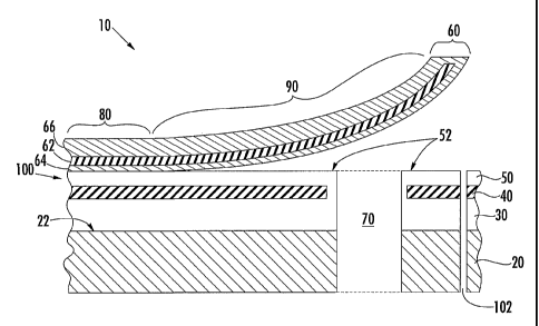
FIG. 1 is a cross-sectional view of a MEMS electrostatic valve in
accordance with an embodiment of the present invention.
FIG. 2 is a top plan view of a MEMS electrostatic valve in accordance with
an embodiment of the present invention.
FIG. 3 is a cross-sectional view of a MEMS electrostatic valve having an
air gap between the substrate and the moveable membrane in accordance with an
embodiment of the present invention.
-6-
CA 02421934 2003-03-11
WO 02/22492 PCT/USO1/28608
FIG. 4 is a cross-sectional view of a MEMS electrostatic valve having a
decreasing air gap between the substrate and the moveable membrane in
accordance with an embodiment of the present invention.
FIG. 5 is a perspective view of a MEMS electrostatic valve array having
individual moveable membranes associated with array apertures in accordance
with an alternate embodiment of the present invention.
FIG. 6 is a perspective view of a MEMS electrostatic valve array having
individual substrate electrodes associated with array apertures in accordance
with
an alternate embodiment of the present invention.
FIG. 7 is a perspective view of a MEMS electrostatic valve array having a
shaped electrode element within the moveable membrane in accordance with an
alternate embodiment of the present invention.
FIGS. ~ - I 1 are cross-sectional views of a MEMS valve construct during
various stages of fabrication in accordance with a method for making
embodiment
1 S of the present invention.
DETAILED DESCRIPTION OF THE INVENTION
The present invention now will be described more fully hereinafter with
reference to the accompanying drawings, in which preferred embodiments of the
invention are shown. This invention may, however, be embodied in many
different
forms and should not be construed as limited to the embodiments set forth
herein;
rather, these embodiments are provided so that this disclosure will be
thorough and
complete, and will fully convey the scope of the invention to those skilled in
the
art. Like numbers refer to like elements throughout.
Referring to FIGS. 1 and 2, a cross-sectional view (FTG. 1) and a top view
of the substrate construct (FIG. 2) of an embodiment of the present invention
provides a MEMS valve device 10 driven by electrostatic forces that can
provide
high and variable flow rates. As shown in FIG.1, the layers of the MEMS valve
device construct are arranged and shown vertically. In a first embodiment, an
electrostatic MEMS valve device comprises in layers, a generally planar
substrate
20, a substrate insulator 30, a substrate electrode 40, a substrate dielectric
50, and a
moveable membrane 60. The substrate defines an aperture 70 formed therethrough
that serves as the valve opening. In the embodiment shown the aperture is
formed
CA 02421934 2003-03-11
WO 02/22492 PCT/USO1/28608
in cooperation with the substrate, the substrate insulator, the substrate
electrode
and the substrate dielectric. In this manner, the aperture may be formed
through
the substrate, the substrate insulator, the substrate electrode and/or the
substrate
dielectric. It is also possible and within the inventive concepts herein
disclosed to
form the aperture in various other configurations that allow for the flowable
media
(i.e. gas, liquid, light, etc.) to enter at one side of the substrate
construct and exit at
the opposite side of the substrate construct. Typically, the aperture will be
cylindrical in shape. However, other shapes such as, a funnel shape having a
smaller perimeter at the valve seat and a larger perimeter at the backside
opening
of the substrate, are also possible and within the breadth of the invention
disclosed.
The movable membrane may be described as having two portions referred
to as the fixed portion 80 and the distal portion 90. The portions are
deposited
horizontally along the length of the moveable membrane. The fixed portion is
substantially affixed to the underlying substrate or intermediate layers at
the
attachment point 100. The distal portion is released from the underlying
substrate
or intermediate layers during fabrication of the MEMS valve device. During
MEMS device operation the distal portion of the device is moveable with
respect
to the underlying substrate and substrate electrode. The movement of the
distal
portion thereby controllably adjusts the portion of the aperture covered by
the
moveable membrane.
In the FIG. 1 cross-sectional view, the moveable membrane 60 comprises
multiple layers including at least one electrode element layer 62 and at least
one
biasing element layer 64 and/or 66. The biasing elements) provide the moveable
membrane with the biased shape shown in FIG.1. Once the moveable membrane
is released from the substrate during fabrication, the biasing element allows
the
overall membrane structure to position itself distant from the substrate. In
the
embodiment shown in FIG. 1 biasing provides for the upward curled shape of the
moveable membrane. Biasing can be accomplished by providing for materials of
dissimilar coefficients of thermal expansion, materials having substantive
differences in cross-sectional thickness or other material characteristics may
also
effect biasing. The electrode element provides the moveable membrane with a
means for electrostatic actuation. In valve operation a voltage is supplied to
the
_g_
CA 02421934 2003-03-11
WO 02/22492 PCT/USO1/28608
electrode element and it is electrostatically attracted toward the substrate
electrode.
As the electrode element comes in contact with the substrate construct, the
moveable membrane forms a valve seal that serves to seal-off the aperture
formed
in the substrate.
The electrostatic MEMS valve device, including the moveable membrane
and underlying substrate layers, is constructed using known integrated circuit
materials and microengineering techniques. Those skilled in the art will
understand that different materials, various numbers of layers, and numerous
arrangements of layers may also be used to form the underlying substrate
layers
and the moveable membrane. Although the MEMS valve device illustrated in the
figures will be used as an example to describe manufacturing details, this
discussion applies equally to all MEMS valve devices provided by the present
invention unless otherwise noted.
Refernng to FIGS. 1 and 2, a substrate 20 defines a generally planar
surface 22 upon which the electrostatic MEMS valve device is constructed.
Preferably the substrate comprises a microelectronic substrate, such as
silicon,
although any suitable substrate material having a generally planar surface can
be
used. The further processing steps involved in the fabrication of the present
invention may be performed at relatively low temperatures and, therefore, the
substrate that is used is not limited to conventional higher temperature
substrates.
By way of example, quartz, glass, or other suitable materials having
insulating
tendencies may serve as the substrate. A substrate insulator layer 30
typically
overlies the planar surface of the substrate and provides electrical
isolation. In
certain embodiments that implement substrate materials having strong
insulation
characteristics it may be possible to form the MEMS valve device without the
substrate insulator layer. The substrate insulator layer preferably comprises
a non-
oxidation-based insulator or polymer, such as polyimide or nitride. In this
application, oxide based insulators are avoided if certain acids (such as
hydrofluoric acid) are used in processing to remove the release layer. The
substrate insulator layer is preferably formed by using a standard deposition
technique, such as conventional spinning or low-pressure chemical vapor
-9-
CA 02421934 2003-03-11
WO 02/22492 PCT/USO1/28608
deposition (LPCVD), to deposit t~~e insulating layer on the planar surface of
the
substrate.
A substrate electrode 40 is deposited as a generally planar layer affixed to
at least a portion of the surface of the underlying substrate insulator layer
30 or
substrate 20. The substrate electrode preferably comprises a gold layer
deposited
on the top surface of the insulator layer. If the substrate electrode is
formed from a
layer of gold, optionally a thin layer of chromium may be deposited prior to
depositing the substrate signal electrode layer to allow better adhesion to
the
insulating layer and/or after the substrate signal electrode layer has been
deposited
to allow better adhesion to any subsequent adjacent materials. Alternatively,
other
suitable metallic or conductive materials may be used for the substrate signal
electrode so long as release layer processing operations does not result in
electrode
erosion. Standard photolithography and etching techniques are typically used
to
deposit the electrode on the surface of the substrate.
1 S Once the substrate electrode has been formed, preferably, a substrate
dielectric layer 50 is deposited on the substrate electrode to provide for a
dielectric
that electrically isolates the substrate signal from the electrode element
found in
the moveable membrane. In embodiments that employ a substrate dielectric
layer,
this layer serves as the valve seat 52 that surrounds the valve aperture. In a
preferred embodiment the substrate dielectric layer will comprise a
resiliently
compressible material. Resiliency for any given material can be assessed by
comparing (a) the ratio of the electrostatic force of the valve around the
aperture to
the valve seat area (i.e. the applied pressure) versus (b) the product of
Young's
modulus (measure of elasticity) for the given material and the ratio of the
surface
roughness of the valve seat to the thickness of the valve seat. The
resiliently
compressible nature of the substrate dielectric layer will allow for the valve
seat to
deform upon contact with the moveable membrane. The deforming characteristic
of the valve seat provides for a sound valve seal to form, thus providing for
improved off flow. One such resiliently compressable substrate dielectric
material
comprises polyimide, although other resiliently compressible dielectric
insulators
or polymers tolerant of release layer processing may also be used. The
substrate
-10-
CA 02421934 2003-03-11
WO 02/22492 PCT/USO1/28608
dielectric layer is formed using a conventional deposition technique, such as
standard spinning techniques or low-pressure chemical vapor deposition LPCVD.
The substrate dielectric layer 50 may be formed with a generally planar
surface (as shown in FIG.1) or the substrate dielectric layer may be formed
with a
textured surface. A textured surface at the valve seat 52 area may be
preferred in
those embodiments in which the moveable membrane "sticks" to the underlying
substrate when release is desired. The MEMS phenomena related to the tendency
of two mating MEMS surfaces to stick together is known in the art as stiction.
By
providing for a textured surface at the valve seat less surface area is
contacting the
moveable membrane when the valve seal is closed and thus less force is
necessary
to overcome the stiction. Textured surfaces are typically formed during
fabrication
and the implementation and fabrication of such surfaces is well known in the
art.
A release layer (not shown in FIGS. 1 and 2), is deposited on the surface of
the substrate dielectric layer 50 in the area generally underneath the distal
portion
of the overlying moveable membrane. The release layer is only deposited on
those
regions below moveable membrane portions not being affixed to the underlying
substrate structure. Preferably, the release layer comprises an oxide or other
suitable material that may be etched away when acid is applied thereto. After
the
overlying layers of the moveable membrane have been deposited on the
substrate,
the release layer may be removed through standard microengineering acidic
etching techniques, such as a hydrofluoric acid etch. When the release layer
has
been removed, the distal portion 90 of moveable membrane 60 is separated from
the underlying surface. The release of the moveable membrane from the
substrate
in conjunction with the biasing characteristics of the biasing element will
typically
result in the thin film membrane having a distal portion that has a curled
shape.
Biasing in the moveable membrane will typically result in the moveable
membrane
curling away from the substrate (as shown in FIG.1) when no electrostatic
force is
applied. It is also possible to bias the moveable membrane such that it curls
toward the substrate when no electrostatic force is applied.
Biasing in the moveable membrane may be accomplished by providing for
biasing element and electrode element materials that differ in thickness,
thermal
coefficient of expansion or any other known biasing characteristic.
Alternately,
-11-
CA 02421934 2003-03-11
WO 02/22492 PCT/USO1/28608
biasing may be induced during fabrication by employing process steps that
create
intrinsic stresses so as to curl the moveable membrane. For example, a
polymeric
biasing element can be deposited as a liquid and then cured by elevated
temperatures so that it forms a solid biasing layer. Preferably, the biasing
element
may comprise a polymer material having a higher thermal coefficient of
expansion
than the electrode element. Next, the biasing element and the electrode
element
are cooled, inducing stresses in the membrane due to differences in the
thermal
coefficients of expansion. The moveable membrane curls because the polymeric
biasing element shrinks faster than the electrode layer.
Additionally, providing differential thermal coefficients of expansion
between the biasing element layers and the electrode element layer can create
bias.
Assuming an increase in temperature, the moveable membrane will curl toward
the
layer having the lower thermal coefficient of expansion because the layers
accordingly expand at different rates. As such, the moveable membrane having
two layers with different thermal coefficients of expansion will curl toward
the
layer having a lower thermal coefficient of expansion as the temperature
rises. In
addition, two polymer film layers having different thermal coefficients of
expansion can be used in tandem with an electrode layer to bias the moveable
membrane as necessary.
The layers of the moveable membrane 60 generally overlie the substrate
electrode 40 and the aperture 70. Known integrated circuit manufacturing
processes are used to construct the layers comprising moveable membrane 60.
The
moveable membrane is comprised of an electrode element and a biasing element.
Preferably, one or more layers of the moveable membrane comprise the electrode
element and one or more additional layers comprise the biasing element. As
shown in FIG. l, one preferred embodiment of the moveable membrane comprises
an electrode element layer 62 positioned between two biasing element layers 64
and 66. It is also possible to configure the moveable membrane with an
electrode
element layer having only one biasing layer positioned on either side of the
electrode element layer. The biasing element layer may also serve as an
insulator
that allows for the complete electrical isolation between the substrate
electrode and
the electrode element of the moveable membrane.
-12-
CA 02421934 2003-03-11
WO 02/22492 PCT/USO1/28608
Preferably, at least one of the layers comprising the moveable membrane is
formed from a flexible material, for instance flexible polymers (i.e. the
biasing
element) and/or flexible conductors (i.e. the electrodes) may be used. In a
preferred embodiment the biasing element will comprise a flexible polymer film
used to hold the moveable membrane in a stationary position absent
electrostatic
forces. In those applications in which the biasing element contacts the
substrate to
form the valve seal it is preferred that the biasing element comprise a
resiliently
compressible material. The resiliently compressible nature of the biasing
element
layer will allow for the valve seal to deform upon contact with the underlying
substrate structure. The deforming characteristic of the contacting biasing
element
surface provides for a sound valve seal to form, thus providing for improved
off
flow. A polymer film material that has resiliently compressible
characteristics may
include a polyimide material, however, other suitable flexible polymers having
resilient characteristics and capable of withstanding the release layer etch
process
can also be employed. In one embodiment both the substrate dielectric layer
and
the biasing element layer of the moveable membrane are formed of a resiliently
compressible material, such as a polyimide material.
The use of polyimide materials in the moveable membrane has been shown
to withstand the pressure generated across the aperture that the membrane is
intended to seal. Additionally, the strength of polyimide materials has shown
to be
resistant to rupturing or blistering even after prolonged use. Calculations
have
showxn that the deflection of a polyimide membrane over a hole having a
circumference of 80 micrometers with a pressure difference of 300 psi is
approximately 0.064 micrometers for a 3 micrometer membrane and 0.22
micrometers for a 2 micrometer membrane. These calculations do not take into
account the electrode element layer that will invariably further limit the
amount of
deflection of the overall moveable membrane.
The electrode element 62 of the moveable membrane 60 preferably
comprises a layer of flexible conductor material. The electrode element may be
deposited directly upon the uppermost planar surface of the substrate
construct and
the release layer or over an optional first biasing layer (i.e. polymer film),
as
needed. The electrode element preferably comprises gold, although other
-13-
CA 02421934 2003-03-11
WO 02/22492 PCT/USO1/28608
conductors tolerant of release layer processing and other flexible materials,
such as
conductive polymer film, may be used. The surface area and/or configuration of
the electrode element can be varied as required to allow for the desired
electrostatic
forces to operate the MEMS valve device. By shaping the electrode element in a
predetermined fashion it is possible to effectuate changes in the valve
release rate.
If gold is used to form the electrode element, a thin layer of chromium may be
deposited onto the electrode element to allow better adhesion of the gold
layer to
the adjacent materials, such as to one or more biasing layers of flexible
polymer
film or the like.
The number of layers, thickness of layers, arrangement of layers, and
choice of materials used in the moveable membrane may be selected to bias the
moveable membrane as required. In particular, the distal portion can be
varyingly
biased as it extends from the fixed portion. The biased position of the distal
portion can be customized individually or collectively to provide a desired
separation from the underlying planar surface and the substrate electrode. For
example, the distal portion can be biased to remain parallel to the underlying
planar surface. Alternatively, the distal portion can be biased to alter the
separation from the underlying planar surface by curling toward or curling
away
from the underlying planar surface. Preferably, the distal portion biased to
curl
away from the underlying substrate and alter the separation therefrom. Those
skilled in the art will appreciate that more than one polymer film layer may
be
used, and that the films may be deposited on either side or both sides of the
electrode elements.
When a voltage is applied between the electrode element of the moveable
membrane and the substrate electrode, the electrostatic force between the
electrode
attracts the flexible electrode element towards the substrate, unrolling the
moveable membrane to effectuate coverage of the aperture. The close proximity
of
the two electrodes when the valve is closed results in a strong electrostatic
force.
This strong electrostatic force results in a valve seal having a low leakage
rate.
When the voltage is removed from the electrodes, the stress in the film causes
the
flexible electrode to curl away from the substrate and open the valves. In the
open
position, since the portion of the membrane that covers the aperture is a
relatively
-14-
CA 02421934 2003-03-11
WO 02/22492 PCT/USO1/28608
large distance from the substrate, large flows through the aperture can be
realized
without flow restrictions.
The valve can be configured so that a pressure difference can be applied in
either direction across the membrane when the membrane seals the aperture. If
the
pressure is coming from the backside of the substrate and pushing up against
the
membrane when the valve is closed, then the pressure will assist in the re-
curling
of the film when the voltage is removed. If, however, the pressure is coming
from
the frontside of the substrate and pushing down against the membrane when it
is
closed, the stress in the membrane will have to work against the applied
pressure to
open the valve. This pressure build-up can be minimized by providing for a
small
aperture through the substrate proximate the end of the distal portion of the
moveable membrane. Since the stress required to curl up the membrane will be
proportional to the overall width of the membrane, the curling stress can be
increased in comparison to the pressure exerted at the small pressure-
relieving
aperture by providing for this small aperture. Once the small pressure-
relieving
aperture has been opened, the pressure differential across the membrane at the
valve aperture will be reduced, making it easier for the stress in the
membrane to
open the valve. An example of such a pressure-relieving aperture 102 is shown
in
FIGS. 1 and 2.
FIG. 3 illustrates a cross-sectional view of an alternative embodiment of
the MEMS electrostatic valve in accordance with the present invention. The
MEMS electrostatic valve 10 of this embodiment has a characteristically
uniform
air gap 110 underlying a medial portion 120 of the moveable membrane 60. The
medial portion of the moveable membrane is defined as the horizontal region
between the fixed portion 80 and the distal portion 90. A release layer (not
shown
in FIG. 3) is deposited on the uppermost layer of the substrate construct in
the area
underlying the medial and distal portions of the moveable membrane. The
release
layer is subsequently removed and results in the overall spatial separation
between
the medial and distal portions of the membrane and the underlying substrate.
The medial portion is constructed generally similar in make-up to the distal
portion and, therefore, the differential in thermal coefficients of expansion
between
the electrode element and the biasing element cause the medial portion to
exhibit
-15-
CA 02421934 2003-03-11
WO 02/22492 PCT/USO1/28608
curling. The curling nature of the moveable membrane is desired for the distal
portion, but is generally undesirable for the medial portion. It is important
to
provide for a predictable medial portion, and thus a predictable air gap,
because
predictability lends itself to improved operating voltage characteristics. To
alleviate the tendency for the medial portion to curl, a bias control layer
130 is
typically provided for that overlies the fixed and medial portions of the
moveable
membrane and structurally constrains the medial portion. Typically, the bias
control layer will overlay the fixed and medial portion of the membrane and
extend
outward, over the sides of the membrane, in order to allow for the bias
control
layer to be anchored to the substrate. The biasing control layer can be formed
from
a metallic material and will generally have a thermal coefficient of expansion
that
differs from the underlying membrane materials so as to hold the medial
portion in
a stationary position. The biasing control layer may be a generally solid
layer, or it
may comprise, lines, grids, cross-hatchings, or other patterns as required to
support
the medial portion and control the shape of the air gap.
Alternatively, the medial portion 120 of the moveable membrane 60 can be
restrained during release by implementing tabs 104 (shown in the plan view
perspective of FIG. 2) on the moveable membrane at the fixed portion 80. The
tabs, which are typically extensions of the layers that comprise the
membranes,
provide an added holding force to insure that a uniform air gap is provided
for
under the medial portion. The tabs may be formed from one or more layers that
comprise the moveable membrane.
FIG. 4 illustrates a cross-sectional view of yet another alternative
embodiment of the MEMS electrostatic valve in accordance with the present
invention. The MEMS electrostatic valve 10 of this embodiment has a
characteristic decreasing air gap 150 underlying a medial portion 120 of the
moveable membrane 60. In this embodiment the cantilevered portion slopes
downward until it contacts the underlying substrate construct at which point
the
moveable membrane transitions into the distal portion and the membrane curls
away from the underlying planar surface. By way of example, the sloping medial
portion may be fabricated by patterning the biasing layer so as to effect a
thin
-16-
CA 02421934 2005-05-13
region at the inflection area 160 or patterning the sloping region of the
medial portion to cause the medial portion to slope toward the substrate.
By predefining the shape of the air gap, recently developed MEMS
electrostatic devices can operate with lower and less erratic operating
voltages. Further discussion of recently development MEMS electrostatic
devices having predefined air gaps is being omitted from this disclosure so
as not to overcomplicate the present invention.
Increased gas or liquid flows can be achieved by creating an array of
apertures defined with a single substrate. FIGS. 5 - 7 illustrate perspective
views of various MEMS electrostatic valve arrays in accordance with further
embodiments of the present invention. FIG. 5 is a MEMS valve array 200
wherein apertures 210 are defined within the substrate 220 in a
predetermined arrangement and each valve aperture has a corresponding
moveable membrane 230. By selectively addressing electrode elements
within the individual membranes variable flow rates can be obtained by
controlling the number of valves opened and closed.
FIG. 6 is a MEMS valve array 250 wherein apertures 210 are defined
within the substrate 220 in a predetermined arrangement and each valve
aperture has a corresponding fixed substrate electrode disposed on the
substrate. By selectively addressing the fixed substrate electrodes 260
within the substrate variable flow rates can be obtained by controlling
the number of valves opened and closed. With a single large moveable
membrane 230 this will typically involve supplying voltage to a rows) of
apertures. Rows in this context are defined as lines of apertures running
perpendicular to the lengthwise direction of the moveable membrane. For
example if electrostatic voltage is supplied to the substrate electrodes
associated with the row of apertures nearest the fixed portion of the valve
structure, the moveable membrane will be pulled down to seal-off
- 17-
CA 02421934 2003-03-11
WO 02/22492 PCT/USO1/28608
these apertures and the remaining distal portion of the membrane will maintain
a
curled position. Additionally, an array of this nature may provide for the
rows of
apertures to be canted, at a slight angle, with respect to the underlying rows
of
substrate electrodes to provide for a greater degree of variable flow as
opposed to
step-like changes in flow. It is also possible and within the inventive
concepts
herein disclosed to configure an array that combines the individual membranes
of
the FIG. 5 embodiment~with the individual substrate electrodes of the FIG. 6
embodiment.
FIG. 7 is a MEMS valve array 270 wherein apertures 210 are defined
within the substrate 220 in a predetermined arrangement and the moveable
membrane 230 has a shaped electrode element 280 (outlined in FIG.7 by the
broken double lines) that allows for the amount of membrane uncurling to be
proportional to the amount of voltage supplied to the electrode element. In
this
regard, supplying full voltage to the electrode element will cause the
moveable
membrane to fully uncurl thus sealing-off all valves in the array. In
instances
where less than full voltage is supplied the membrane may uncurl partially,
thus
sealing-off only those valves underlying the uncurled portion of the membrane.
The shape of the electrode element is shown by way of example. The shape of
the
electrode element will be predetermined based upon size of the moveable
membrane, size of the array and the configuration of the array. Alternately,
the
shaped electrode can be the substrate electrode. Shaping the substrate
electrode, as
opposed to the membrane electrode, may be preferred to insure uniform curl in
the
moveable membrane.
Additionally, the present invention provides for a method of making a
MEMS valve device driven by electrostatic forces. FIGS. 8-11 illustrate
various
stages in the fabrication of the MEMS electrostatic valve, in accordance with
a
method of making embodiment of the present invention. This method, in which
initial aperture formation commences prior to the valve construction and is
completed after valve construction, has the advantage of allowing the
alignment
between the aperture and the surrounding substrate electrode to be performed
on
the frontside of the substrate construct. Since the moveable membrane needs to
be
formed so that it overlies the aperture, the final opening of the aperture
will be
-18-
CA 02421934 2003-03-11
WO 02/22492 PCT/USO1/28608
completed after the formation of the membrane. The thin film nature of the
fabrication technology requires that the build surfaces be generally flat
prior to
forming the substrate electrode and the flexible electrode element of the
membrane.
FIG. 8 is an illustration of a cross-sectional view of a substrate 300 that
has
undergone backside etch to define a large cavity 310 and front side etch to
define
valve apertures 320. Initially, a large cavity may be defined in the backside
of the
substrate. Typically, a conventional wet etch process will be used to form the
large
cavity. The large cavity, typically, results in thinning the substrate down to
approximately 50 micrometers, although other desirable thicknesses are also
possible. The large cavity etch process is an optional process that provides
for
minimization of flow restrictions and simplifies the subsequent formation of
the
valve apertures. After the large cavity is formed, the valve apertures are
etched
partially through the frontside of the substrate. Typically a reactive ion
etch (RIE)
process will used to perform the precision etching required of the valve
apertures.
A sacrificial plug material 330 is then disposed in the apertures to
facilitate a
continuous substrate layer upon which the valve can be constructed. The
sacrificial plug material will typically comprise copper or any other suitable
material may be used as the sacrificial plug material. Once the plug material
has
been disposed, it is typically subjected to a polishing procedure to assure
planarization of the surface and ready the substrate for valve construction.
FIG. 9 depicts a cross-sectional view of the MEMS valve construct after
the valve structure has been formed on the frontside surface of the substrate.
Typically, the formation of the valve structure will include disposing an
insulator
layer 340 on the substrate; disposing, patterning and etching a substrate
electrode
layer 350 on the insulator layer; and disposing a dielectric layer 360 on the
substrate electrode layer. The formation of these layers is followed by the
formation of a release layer 370, typically an oxide that will subsequently be
removed to facilitate release of a portion of the membrane from the substrate.
The
membrane 380 is then disposed on the release layer and anchored to the
substrate
via the dielectric layer. In the embodiment shown, the membrane comprises a
first
biasing element/dielectric layer 390 disposed on the release layer and the
dielectric
-19-
CA 02421934 2003-03-11
WO 02/22492 PCT/USO1/28608
layer, an electrode element layer 400 disposed on the first biasing
element/dielectric layer and a second biasing element layer 410 disposed on
the
electrode. These valve construct layers and fabrication steps are shown by way
of
example, other layering sequences are possible and within the inventive
concepts
herein disclosed. The surfaces that will eventually form the valve seat and
the
valve cover may be textured surfaces to allow for the MEMS device to overcome
common release problems related to stiction. In the embodiment shown it may be
desirable to texture the dielectric layer 360 and/or the first biasing
element/dielectric layer 390. The texturing of these surfaces can be
accomplished
in conjunction with the deposition and removal of the release layer. The
process of
texturing a surface on a MEMS device is well known by those of ordinary skill
in
the art.
FIG. 10 illustrates a cross-sectional view of the MEMS valve construct
after the backside of the substrate has been etched to expose the plug
material, the
plug material is removed and the aperture 320 has been etched to expose the
release layer. The backside etch of the substrate is typically performed with
a wet
etch process. Once the etch process exposes the backside of the sacrificial
plug
material, the plug is removed by performing an etch process. Typically, the
plug
material will be removed by a conventional wet etch process. After the plug
material has been removed, the aperture is furthered formed into the valve
construct up to the release layer 370. A reactive ion etch process will,
typically, be
used to further form the aperture and insure that the aperture has precision
facings.
FIG. 11 shows the completed MEMS valve construct after the release layer has
been removed, thus, allowing for the distal portion of the membrane to be
released
from the substrate.
This method, in which initial aperture formation commences prior to the
valve construction and is completed after valve construction, has the
advantage of
allowing the alignment between the aperture and the surrounding substrate
electrode to be performed on the frontside of the substrate construct.
Many modifications and other embodiments of the invention will come to
mind to one skilled in the art to which this invention pertains having the
benefit of
the teachings presented in the foregoing descriptions and the associated
drawings.
-20-
CA 02421934 2003-03-11
WO 02/22492 PCT/USO1/28608
Therefore, it is to be understood that the invention is not to be limited to
the
specific embodiments disclosed and that modifications and other embodiments
are
intended to be included within the scope of the appended claims. Although
specific
terms are employed herein, they are used in a generic and descriptive sense
only
and not for purposes of limiting the scope of the present invention in any
way.
-21-