Note: Descriptions are shown in the official language in which they were submitted.
CA 02422712 2003-03-12
WO 02/32205 PCT/US01/30709
1
COMPOUND WAVEFORM GASKET FOR LOW CLOSURE
FORCE EMI SHIELDING APPLICATIONS
BACKGROUND OF THE INVENTION
The present invention relates broadly to gaskets for providing environmental
sealing
and/or electromagnetic interference (EMI) shielding, and particularly to a low
closure force EMI
shielding gasket which is especially adapted for use within small electronics
enclosures such as
cellular phone handsets and other handheld electronic devices.
The operation of electronic devices such as televisions, radios, computers,
medical
instruments, business machines, communications equipment, and the like is
attended by the
generation of electromagnetic radiation within the electronic circuitry of the
equipment. As is
detailed in U.S. Patent Nos. 5,202,536; 5,142,101; 5,105,056; 5,028,739;
4,952,448; and
4,857,668, such radiation often develops as a field or as transients within
the radio frequency band
of the electromagnetic spectrum, i.e., between about 10 KHz and 10 GHz, and is
termed
"electromagnetic interference" or "EMI" as being known to interfere with the
operation of other
proximate electronic devices.
To attenuate EMI effects, shielding having the capability of absorbing and/or
reflecting
EMI energy may be employed both to confine the EMI energy within a source
device, and to
insulate that device or other "target" devices from other source devices. Such
shielding is
provided as a barrier which is inserted between the source and the other
devices, and typically is
configured as an electrically conductive and grounded housing which encloses
the device. As the
circuitry of the device generally must remain accessible for servicing or the
like, most housings are
provided with openable or removable accesses such as doors, hatches, panels,
or covers. Between
even the flattest of these accesses and its corresponding mating or faying
surface, however, there
may be present gaps which reduce the efficiency of the shielding by presenting
openings through
which radiant energy may leak or otherwise pass into or out of the device.
Moreover, such gaps
represent discontinuities in the surface and ground conductivity of the
housing or other shielding,
and may even generate a secondary source of EMI radiation by functioning as a
form of slot,
antenna. In this regard, bulk or surface currents induced within the housing
develop voltage
gradients across any interface gaps in the shielding, which gaps thereby
function as antennas
which radiate EMI noise. In general, the amplitude of the noise is
proportional to the gap length,
with the width of the gap having less appreciable effect.
CA 02422712 2003-03-12
WO 02/32205 PCT/US01/30709
2
For filling gaps within mating surfaces of housings and other EMI shielding
structures,
gaskets and other seals have been proposed both for maintaining electrical
continuity across the
structure, and for excluding from the interior of the device such contaminates
as moisture and dust.
Such seals are bonded or mechanically attached to, or press-fit into, one of
the mating surfaces,
and function to close any interface gaps to establish a continuous conductive
path thereacross by
conforming under an applied pressure to irregularities between the surfaces.
Accordingly, seals
intended for EMI shielding applications are specified to be of a construction
which not only
provides electrical surface conductivity even while under compression, but
which also has a
resiliency allowing the seals to conform to the size of the gap. The seals
additionally must be wear
resistant, economical to manufacture, and capability of withstanding repeated
compression and
relaxation cycles. For further information on specifications for EMI shielding
gaskets, reference
may be had to Severinsen, J., "Gaskets That Block EMI," Machine Design, Vol.
47, No. 19, pp.
74-77 (August 7, 1975).
EMI shielding gaskets typically are constructed as a resilient core element
having gap-
filling capabilities which is either filled, sheathed, or coated with an
electrically conductive
element. The resilient core element, which may be foamed or unfoamed, solid or
tubular, typically
is formed of an elastomeric thermoplastic material such as polyethylene,
polypropylene, polyvinyl
chloride, or a polypropylene-EPDM blend, or a thermoplastic or thermosetting
rubber such as a
butadiene, styrene-butadiene, nitrile, chlorosulfonate, neoprene, urethane, or
silicone rubber.
Conductive materials for the filler, sheathing, or coating include metal or
metal-plated
particles, fabrics, meshes, and fibers. Preferred metals include copper,
nickel, silver, aluminum,
tin or an alloy such as Monel, with preferred fibers and fabrics including
natural or synthetic fibers
such as cotton, wool, silk, cellulose, polyester, polyamide, nylon, polyimide.
Alternatively, other
conductive particles and fibers such as carbon, graphite, or a conductive
polymer material may be
substituted.
Conventional manufacturing processes for EMI shielding gaskets include
extrusion,
molding, or die-cutting, with molding or die-cutting heretofore being
preferred for particularly
small or complex shielding configurations. In this regard, die-cutting
involves the forming of the
gasket from a cured sheet of an electrically-conductive elastomer which is cut
or stamped using a
die or the like into the desired configuration. Molding, in turn, involves the
compression or
injection molding of an uncured or thermoplastic elastomer into the desired
configuration.
CA 02422712 2008-12-03
3
More recently, a form-in-place (FIP) process has been proposed for the
manufacture of EMI shielding gaskets. As is described in commonly-assigned
U.S.
Patent Nos. 6,096,413; 5,910,524; and 5,641,438, and PCT Application WO
96/22672; and in U.S. Patent Nos. 5,882,729 and 5,731,541; and Japanese Patent
Publication (Kokai) No. 7177/1993, such process involves the application of a
bead of
a viscous, curable, electrically-conductive composition which is dispensed in
a fluent
state from a nozzle directly onto a surface of a substrate such as a housing
or other
enclosure. The composition, typically a silver-filled or otherwise
electrically-conductive
silicone elastomer, then is cured-in-place via the application of heat or with
atmospheric moisture or ultraviolet (UV) radiation to form an electrically-
conductive,
elastomeric EMI shielding gasket in situ on the substrate surface.
Another recent EMI shielding solution for electronics enclosures, which
solution
is further described in commonly-assigned U.S. Patent No. 5,566,055 and in DE
19728839 involves the over-molding of the housing or cover with an conductive
elastomer. The elastomer is integrally molded in a relatively thin layer
across the
inside surface of the housing or cover, and in a relatively thicker layer
along the
interface locations thereof providing both a gasket-like response for
environmentally
sealing the cover to the housing and electrical continuity for the EMI
shielding of the
enclosure. The elastomer additionally may be molded onto interior partitions
of the
cover or housing, or itself molded. to integrally-form such partitions,
providing
electromagneticly-isolated compartments between potentially interfering
circuitry
components. Covers of such type are marketed commercially under the name Cho-
Shield Cover by the Chomerics EMC Division of Parker-Hannifin Corporation
(Woburn,
MA).
Yet another solution for shielding electronics enclosures, and particularly
the
smaller enclosures typical of cellular phone handsets and other handheld
electronic
devices, concerns the incorporation of a thin plastic retainer or frame as a
supporting
member of the gasket. As is described in commonly-assigned, U.S. Patent No.
5,641,438, the electrically conductive elastomer may be molded or, as is
described in
U.S. Patent No. 5,731,541, formed-in-place or otherwise attached to the inner
or inner
peripheral edge surfaces and/or to the upper or lower face surfaces of the
frame. So
constructed, the gasket and frame assembly may be integrated within the
electronic
device to provide a low impedance pathway between, for example, peripheral
ground
traces on a printed circuit board (PCB) of the device, and other components
thereof
such as the conductive coating of a plastic housing, another PCB, or a keypad
assembly. Uses for the spacer gaskets of the type herein include EMI shielding
CA 02422712 2008-12-03
4
applications within digital cellular, handyphone, and personal communications
services
(PCS) handsets, PC cards (PCMCIA cards), global positioning systems (GPS),
radio
receivers, and other handheld devices such as personal digital assistants
(PDAs).
Other uses include as replacements for metal EMI shielding "fences" on PCBs in
wireless telecommunication devices.
Requirements for typical small enclosure applications generally specify a low
impedance, low profile connection which is deflectable under relatively low
closure
force loads, e.g., about 1.0-8.0 lbs per inch (0.2-1.5 kg per cm) of gasket
length.
Usually, a minimum deflection, typically of about 10%, also is specified to
ensure that
the gasket sufficiently conforms to the mating housing or board surfaces to
develop an
electrically conductive pathway therebetween. It has been observed that for
certain
applications, however, that the closure or other deflection force required to
effect the
specified minimum deflection of conventional profiles may be higher than can
be
accommodated by the particular housing or board assembly design.
One method of achieving a lower closure force gasket design particularly
adapted for use in smaller electronic enclosure packages has been to form the
gasket
as having a periodic "interrupted" pattern of alternating local maxima and
minima
heights. Conventionally, and as is described in commonly-assigned U.S. Patent
No.
6,121,545 in the Technical Publication "EMI Shielding and Grounding Spacer
Gasket,"
Parker Chomerics Division, Woburn, MA (1996), and in PCT application 98/54942,
gaskets of such type may be formed by molding or the FIP process as having a
crenelated, i.e., notched, serrated, or a sinusoidal "waveform" profile, or as
a series of
discrete beads. In general, for a specified joint configuration, a gasket
having such an
"interrupted" profile or pattern would be expected to exhibit a greater
deflection under
a given compressive load than a continuous profile.
A commercial waveform gasket assembly representative of the existing state of
the art is shown generally at 1 in the perspective view of Fig. 1 and in the
top view of
Fig. 2 as including a length of electrically-conductive, elastomeric gasket 2,
which may
be formulated as a silver or silver-plated-filled silicone or fluorosilicone
material, which
is bonded by injection or compression molding along a landed edge, referenced
at 3 in
Fig. 1, of a housing 4. Housing 4 may be formed of a plastic material such as
ABS,
polycarbonate, nylon, polyester, polyetherimide, a liquid crystal polymer
(LCP), or the
like which is provided with a metallized coating to render the interior
surface, 5,
thereof electrically-conductive. Alternatively, housing 4 may be formed of a
relatively
lightweight metal such as magnesium or aluminum.
In basic geometry, the distal edge, 6, of gasket 2 assumes a generally
CA 02422712 2008-12-03
sinusoidal profile. Functionally, the elastomeric gasket 2 deforms via a
compression
mode with the troughs of the waveform acting as compression stops. Such
deformation response of gasket 2 is illustrated in Fig. 3 wherein a 3-D mesh
model of
a cross-section thereof is shown in phantom at 7 in an uncompressed or normal
5 orientation which is superimposed over the deformed or stressed orientation
referenced at 8 assumed upon the compression of gasket 2 between the edge
surface
3 (not shown in Fig. 3) and a faying interface surface, represented by the
plane
referenced in phantom at 9. As is confirmed in Fig. 3, gasket 2 exhibits a
deformation
response which is mainly in compression, with the darker areas of shading
indicating
regions of increasing compressive stress.
As the sizes of handheld electronic devices such as cellular phone handsets
has
continued to shrink, it will be appreciated that further improvements in the
design of
gaskets profiles therefor would be well-received by the electronics industry.
Especially
desired would be a low closure force gasket profile which is adapted for use
in the
smaller electronics enclosures which are increasingly becoming the industry
standard.
BROAD STATEMENT OF THE INVENTION
The present invention is directed to a low closure force gasket for
environmental sealing and/or electromagnetic interference (EMI) shielding
which is
especially adapted for use in smaller electronic enclosure packages. As in
conventional
designs, the gasket of the present invention is configured as having an apex
surface
which is formed, relative to the housing or other substrate on which the base
of the
gasket may be supported, to exhibit a sinusoidal or other "waveform" profile
to be
responsive to lower closure force loads when compressed intermediate a pair of
surfaces such as between two halves of a housing. However, the gasket of the
invention further is configured, such as in having, for example, at least one
lateral
surface which is formed, relative to the apex surface, as a transverse
waveform
profile, to exhibit a controlled deflection response which may be
characterized as a
bending moment. Such response advantageously provides a large but controlled
deflection affording a more uniform interface contact with the contacting
surface for
more assured electrical and physical continuity and, in turn, more reliable
EMI
shielding and environmental sealing effectiveness. When employed, for example,
in
electronics applications, the gasket of the invention therefore provides
consistent EMI
shielding and, additionally, environmental sealing effectiveness.
CA 02422712 2003-03-12
WO 02/32205 PCT/US01/30709
6
Advantages of the present invention therefore include the provision of an
improved gasket
profile for low closure force applications such as may be found in small,
handheld electronic
devices. Additional advantages includes a gasket profile which exhibits a
controlled deflection
response for more stable interface contact with the housing or circuit board
components of the
enclosure and, in turn, more assured electrical continuity and reliable EMI
shielding effectiveness.
These and other advantages will be readily apparent to those skilled in the
art based upon the
disclosure contained herein.
BRIEF DESCRIPTION OF THE DRAWINGS
For a fuller understanding of the nature and objects of the invention,
reference should be
had to the following detailed description taken in connection with the
accompanying drawings
wherein:
Fig. 1 is a perspective end view, partly in cross-section, of a portion of a
housing for a
handheld electronic communication device having molded on an edge thereof a
"waveform" EMI
shielding gasket representative of the prior art;
Fig. 2 is a top view of the housing of Fig. 1;
Fig. 3 is 3-D mesh model of a cross-section of the prior art waveform gasket
of Fig. 1
showing the compression response thereof;
Fig. 4 is a perspective view end view, partly in cross-section, of a portion
of a
representative EMI shielding assembly which includes a housing part along the
edges of which is
molded one embodiment of a combination waveform gasket in accordance with the
present
invention;
Fig. 5 is a magnified view rotated 90 of the EMI shielding assembly of Fig.
4;
Fig. 6 is a further magnified view of the EMI shielding assembly of Fig. 5
showing the
cross-section of the waveform gasket of the present invention in enhanced
detail;
Fig. 7 is 3-D mesh model of a cross-section of the waveform gasket of Fig. 6
showing the
deflection response thereof;
Fig. 8 is a plot comparing the force-deflection responses of the combination
waveform
gasket of Fig. 7 according to the present invention to a similarly-dimensioned
non-waveform
gasket;
CA 02422712 2003-03-12
WO 02/32205 PCT/US01/30709
7
Fig. 9A is a 3-D graphical representation of a finite element model of the
predicted stress
distribution at 0.020-inch (0.50 mm) deflection in a representative waveform
gasket profile of the
present invention;
Fig. 9B is a 3-D graphical representation of the stress distributions of the
gasket profile of
Fig. 9A at 0.025-inch (0.635 mm) deflection;
Fig. 10A is a 3-D graphical representation of a finite element model of the
stress
distributions at 0.020-inch (0.50 mm) deflection in an alternative embodiment
of a waveform
gasket profile of the present invention;
Fig. lOB is a 3-D graphical representation of the stress distributions of the
gasket profile
of Fig. 10A at 0.025-inch (0.635 mm) deflection; and
Fig. 11 is a plot comparing the force-deflection responses of the combination
waveform
gasket of Fig. 9 according to the present invention to the conventional
waveform gasket of Fig. 1.
The drawings will be described further in connection with the following
Detailed
Description of the Invention.
DETAILED DESCRIPTION OF THE INVENTION
Certain terminology may be employed in the description to follow for
convenience rather
than for any limiting purpose. For example, the terms "forward," "rearward,"
"right," "left,"
"upper," and "lower" designate directions in the drawings to which reference
is made, with the
terms "inward >" "inner>" or "inboard" and "outward," "outer," or "outboard"
referring
,
respectively, to directions toward and away from the center of the referenced
element, and the
terms "radial" and "axial" referring, respectively, to directions
perpendicular and parallel to the
central longitudinal axis of the referenced element. Terminology of similar
import other than the
words specifically mentioned above likewise is to be considered as being used
for purposes of
convenience rather than in any limiting sense.
In the figures, elements having an alphanumeric designation may be referenced
herein
collectively or in the alternative, as will be apparent from context, by the
numeric portion of the
designation only. Further, the constituent parts of various elements in the
figures may be
designated with separate reference numerals which shall be understood to refer
to that constituent
part of the element and not the element as a whole, General references, along
with references to
spaces, surfaces, dimensions, and extents, rnay be designated with arrows.
CA 02422712 2003-03-12
WO 02/32205 PCT/US01/30709
8
For the purposes of the discourse to follow, the precepts of the invention
herein involved
are described in connection with the molding or other application of an
elastomeric, electrically-
conductive, electromagnetic interference (EMI) shielding gasket onto an edge
or other surface of
one part of an enclosure for a handheld electronic device such as a cellular
telephone. In view of
the discourse to follow, however, it will be appreciated that aspects of the
present invention may
find utility in other EMI shielding applications, such as for spacer frame
gaskets, circuit boards, or
EMI shielding caps, or in non-electrically-conductive and/or thenmally-
conductive embodiments
for environmental sealing and/or heat transfer applications. Use within those
such other
applications therefore should be considered to be expressly within the scope
of the present
invention.
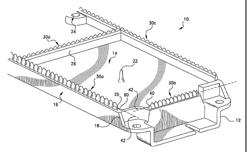
Referring then to the figures, an exemplary sealing assembly for EMI shielding
applications is shown generally at 10 in Fig. 4 as including a housing part or
other enclosure, 12,
for an electronic device which may be a cellular telephone or, alternatively
another handheld or
other electronic device such as a personal communications services (PCS)
handset, PCMCIA card,
global positioning system (GPS), radio receiver, personal digital assistant
(PDA), or the like.
Housing part 12 has an inner surface, 14, and an outer surface, 16, which
extend to form sides
walls, one of which is referenced at 18, therebetween having a peripheral edge
surface, 20. Edge
surface 20 functions as an interface surface with a faying edge or other
interfacing surface of a
mating housing part (not shown). For assuring the positive positioning of the
mating parts, each of
the parts may be formed as having one or more positioning pins, one of which
is referenced at 22
on part 12, receivable within a corresponding hole, such as the hole 24 of
part 12, provided in the
mating housing part. Typically, the interior of the housing part 12 is divided
into to more separate
cavities, such as by an internal wall, 26, for providing electromagnetically
isolated compartments
between potentially interfering circuitry.
For many applications, housing part 12 may be injection or otherwise molded of
a
thermoplastic or other polymeric material such as a poly(ether ether ketone),
polyiniide, high
molecular weight polyethylene, polypropylene, polyetherimide, polybutylene
terephthalate, nylon,
fluoropolymer, polysulfone, polyester, ABS, acetal homo or copolymer, or a
liquid crystal
polymer. In the case of an electrically-nonconductive material, the housing
part inner surface 14
may be painted, metallized, or otherwise provided with a metal or metal-filled
coating layer.
Alternatively, housing part 12 may be forrned of a relatively lightweight
metal such as magnesium
or aluminum.
CA 02422712 2003-03-12
WO 02/32205 PCT/US01/30709
9
As may be seen with additional reference to the magnified views of Figs. 5 and
6, a
resilient gasket, the constitute segments of which are referenced at 30a-d, is
molded or otherwise
retained, such as by adhesive bonding or an interference fit, on side wall 18
and optionally,
internal wal126, to be compressible axially under a predetermined compressive
load intermediate
edge surface 20 and the corresponding surface of the mating housing part (not
shown in Figs. 4-6).
In this regard, gasket 30 preferably is overmolded onto the sidewall edge
surface 20 by injection or
compression molding as formed of an elastomeric material which specifically
may be selected for
temperature, chemical, or physical compatibility with the housing material.
Depending then upon
the application, suitable materials may include natural rubbers such as Hevea,
as well as
thermoplastic, i.e., melt-processible, or thermosetting, i.e., vulcanizable,
synthetic rubbers such as
fluoropolymers, chlorosulfonate, polybutadiene, polybutadiene, buna-N, butyl,
neoprene, nitrile,
polyisoprene, silicone, fluorosilicone, copolymer rubbers such as ethylene-
propylene (EPR),
ethylene-propylene-diene inonomer (EPDM), nitrile-butadiene (NBR) and styrene-
butadiene
(SBR), or blends such as ethylene or propylene-EPDM, EPR, or NBR. The term
"synthetic
rubbers" also should be understood to encompass materials which alternatively
may be classified
broadly as thermoplastic or thermosetting elastomers such as polyurethanes,
silicones,
fluorosilicones, styrene-isoprene-styrene (SIS), and styrene-butadiene-styrene
(SBS), as well as
other polymers which exhibit rubber-like properties such as plasticized
nylons, polyesters, ethylene
vinyl acetates, and polyvinyl chlorides. As used herein, the term
"elastomeric" is ascribed its
conventional meaning of exhibiting rubber-like properties of compliancy,
resiliency or
compression deflection, low compression set, flexibility, and an ability to
recover after
deformation.
Preferably for EMI shielding applications, the elastomeric material is
selected to be a
silicone or fluorosilicone material. In general, silicone elastomers exhibit
desirable properties such
as thermal and oxidation resistance over a wide temperature range, as well as
resistance to many
chemicals and to weather effects. These materials further exhibit excellent
electrical properties
including resistance to corona breakdown over a wide range of temperatures and
humidity.
For EMI shielding applications, the silicone or other elastomeric material may
be rendered
electrically conductive for providing an electrically conductive pathway
between the interfacing
surfaces via the loading of a continuous binder phase of the material with an
electrically-
conductive filler. Suitable electrically-conductive fillers include nickel and
nickel-plated
substrates such as graphite and noble metals, and silver and silver-plated
substrates such as: pure
CA 02422712 2003-03-12
WO 02/32205 PCT/US01/30709
silver; silver-plated noble metals such as silver-plated gold; silver-plated
non-noble metals such as
silver-plated copper, nickel, aluminum, and tin; and silver-plated glass,
ceramics, plastics,
elastomers, and mica; and mixtures thereof. The shape of the filler is not
considered critical to the
present invention, and may include any shape that is conventionally involved
in the manufacture or
5 formulation of conductive materials of the type herein involved including
solid spheres, hollow
microspheres, elastomeric balloons, flakes, platelets, fibers, rods, or
irregularly-shaped particles.
Similarly, the particle size of the filler is not considered critical, but
generally will be in the range
of from about 0.250-250 m, with a range of from about 0.250-75 m being
preferred.
The filler is loaded in the composition in a proportion sufficient to provide
the level of
10 electrical conductivity and EMI shielding effectiveness in the cured gasket
which is desired for the
intended application. For most applications, an EMI shielding effectiveness of
at least 10 dB, and
preferably at least 20 dB, and most preferably at least 100 dB or higher, over
a frequency range of
from about 10 MHz to 12 GHz is considered acceptable. Such effectiveness
translates to a filler
proportion which generally is between about 10-80% by volume, based on the
total volume of the
reaction system, and preferably is between about 20-70% by volume. As is
known, however, the
ultimate shielding effectiveness of the cured gasket will vary based on the
amount of electrically-
conductive material in the filler and the imposed load or deflection,
typically between about 10-
50%, of the gasket.
Alternatively, the electrically conductive filler may be provided as a
relatively thin, i.e., 1-
10 mils (0.025-0.25 mm), platirig or coating layer covering gasket 30. In the
case of a coating,
such layer may be formulated as a silicone, fluorosilicone, or other
elastomeric binder which forms
a continuous phase within which the filler is dispersed.
Returning to Figs. 4-6, it may be seen that in the uncompressed or normal
state shown, the
constituent segments 30a-b of gasket 30 each is formed as an elongate body,
40, of an indefinite
length which extends along a longitudinal axis, which axis is shown as the
central axis commonly
referenced at 42 for the gasket segments 30a and 30b. Depending upon the
configuration of
housing part 12, gasket 30 and, accordingly, body 40 thereof may be continuous
or discontinuous,
and may trace a linear, curved, rectilinear, curvilinear, or other shape path
along longitudinal axis
42.
With particular reference to the magnified views of Figs. 5 and 6, body 40 may
be seen to
be configured in accordance with the precepts of the present invention as
having a compound
waveform profile which effects a controlled deflection response in the gasket
30. In basic
CA 02422712 2008-12-03
11
construction, such profile includes a base or bottom surface, 50, an apex or
top surface,
52, which defines the first waveform profile, a portion of which is referenced
at 53, of
the gasket 30, an inboard lateral surface, 54, and an outboard lateral
surface, 56,
which is disposed opposite the inboard lateral surface 54 and which defines
the second
waveform profile of the gasket. As may be seen, all of the surfaces 50, 52,
54, and 56
may be integrally formed within body 40.
Base surface 50 in the illustrated configuration of gasket 30 is generally
planar
and extends generally parallel to the housing part edge surface 20 along the
length of
the gasket body 40. With gasket 30 being molded or otherwise bonded or
attached to
the edge surface 20, base surface 50 thereby proximal supports the gasket on
the
surface 20 for compression therebetween and the faying interface surface (not
shown in
Figs. 5 and 6) of, for example, the mating housing part. Depending, however,
on the
geometry or orientation of the edge surface 20, base surface 50 alternatively
may be
configured, for example, as being beveled or chamfered to correspond to any
beveling
or chamfering of the inboard ' corner 60 of surface 20. Moreover in the
illustrative
embodiment of Figs. 5 and 6, base surface 50 further is formed as having an
extension
portion, which may be best seen in phantom at 62 in Fig. 6, depending
therefrom, that
is bonded or otherwise secured to the inner surface 14 of the side wall 18. It
will be
understood that extension portion 62 provides additional surface area as well
as a shear
surface attachment for further securing, such as by self-adhesive molding or
adhesive
bonding, the gasket body 40 to the housing part 12.
Apex surface 52 extends radially from longitudinal axis 42 as spaced-
apart from base surface 50 for distal contact with the faying interface
surface
(not shown). In the illustrated embodiment of Figs. 5 and 6, apex surface 52
defines
the first waveform profile 53 of gasket 30 as extending along longitudinal
axis 42 in a
first periodic series of alternating first high amplitude intervals or crests,
one of which is
referenced at 70, and first low amplitude intervals or troughs, one of which
is
referenced at 72. The first waveform profile 53 defined by apex surface 52 may
be of
any pattern, such as square-wave, ramp, or sawtooth, but in the illustrated
embodiment of Fig. 6 is shown to generally be sinusodial and as having a
given,
preferably constant, wavelength, referenced at A1i which may be between about
0.01-
0.50 inches (0.25-12.7 mm) for many applications, and a crest height, h, or
double
wave amplitude, which may be between about 0.005-0.50 inches (0.13-12.7 mm).
For
EMI shielding applications, wavelength A1r and accordingly the gaps between
the crests
70, may be sized with respect to the wavelength of the incident EMI radiation,
such as
less than about 1/4 of that wavelength for frequencies in the range of 10 MHz-
10
CA 02422712 2003-03-12
WO 02/32205 PCT/US01/30709
12
GHz, to maintain the required level of EMI shielding. Moreover for EMI
shielding applications, it
is preferred that a minimum electrical resistivity, typically about 0.1 SZ or
less, is maintained per
unit length of the gasket 30.
Inboard lateral surface 54 extends intermediate the base and apex surfaces 50
and 52 in
forming one side of the gasket body 40. With the other side of the gasket body
40 being formed
by the outboard lateral surface 56, a widthwise extent, referenced at w in
Fig. 6, of the apex
surface 52 is defined therebetween which, for ease of manufacturing the mold
or other tooling for
gasket 30.via a CNC or wirecut EDM process, may be maintained as generally
constant. For
assisting in the control of the deflection of the gasket 30 in the manner to
be described hereinafter,
inboard lateral surface 54 may be configured so as to assume a generally
concave profile along
axis longitudinal axis 42 intermediate the base and apex surfaces 50 and 52 in
having a radius of
curvature, referenced at rl in Fig. 6, about the axis 74 which extends
generally parallel to
longitudinal axis 42. Radius rl typically may be between about 0.002-0.20
inches (0.05-5.8 mm)
for may of the applications herein involved.
Outboard lateral surface 56, in turn, similarly extends intermediate the base
surface and
apex surfaces 50 and 52 opposite the inboard lateral surface 54. As may be
seen with reference to
the enhanced view of Fig. 6, outboard lateral surface 56 preferably is
inclined along axis 76 from
the base surface 50 to the apex surface 52 in the direction of the inboard
lateral surface 54 so as to
form an acute angle, referenced at 0, with a vertical axis, 78. Such
inclination of the lateral surface
56 further assists in the controlled deflection of the gasket 30 as will be
described hereinafter.
In accordance with the precepts of the present invention, outboard lateral
surface 56 is
configured as defining a second waveform profile of the gasket 30. As may be
seen best in Fig. 5,
such profile, referenced generally at 80 in Fig. 5, is disposed generally
transverse to the first
waveform profile 53 of apex surface 52 and extends along longitudinal axis 42
in a second
periodic series of alternating second high amplitude intervals or crests, one
of which is referenced
at 82 in Fig. 5, and second low amplitude intervals or troughs, one of which
is referenced at 84 in
Fig. 5. The second waveform profile 80 defined by outboard lateral surface 56
again may be of
any pattern, such as square-wave, ramp, or sawtooth, and may be the same as or
different from the
pattern of the first waveform 53 profile of apex surface 52. In the
illustrated embodiment of Fig.
5, however, the second waveform profile 80 is also shown to be generally
sinusoidal in having a
convex curvature, such as about a central inclined axis, 86, in the direction
indicated by arrow 88
intermediate each successive pair of troughs 84. Each such trough pair also
defines a preferably
CA 02422712 2003-03-12
WO 02/32205 PCT/US01/30709
13
constant wavelength, referenced at X2, therebetween which, in the embodiment
of Fig. 5 is about
equal to X1 (Fig. 6) of the first waveform profile 53. Preferably, each crest
82 of the second
waveform profile 80 is in registration with a corresponding crest 70 of the
first waveform profile
53, and each trough 84 of the second waveform profile 80 is in registration
with a corresponding
trough 72 of the first waveform profile 53 such the first and second waveform
profiles are
generally in phase along longitudinal axis 42.
By virtue of the provision of a combination of waveform profiles, gasket 30 of
the
invention is thereby made to exhibit a controlled deflection response when
deformed under an
axially-directed force between, for example, the edge surface 20 of housing
part 12 and a faying
interface surface from a mating housing part or other component. Such
deformation response of
gasket 30 is illustrated in Fig. 7 wherein a 3-D mesh model of a cross-section
of gasket 30 is
shown in phantom at 90 in an uncompressed or normal orientation which is
superimposed over the
deformed or stressed orientation referenced at 92 assumed upon the compression
of gasket 30
between the interfacing surfaces 94 and 96. As may be seen in Fig. 7, the
controlled deflection
response 92 of gaslcet 30 is characterized in that the gasket body 40 is
angularly deflected, i.e.,
bent or folded, intermediate the base and apex surfaces 50 and 52 thereof
about a corresponding
bending or moment arm in the radial direction referenced by arrow 98. The
darker areas of
shading in the figure indicate regions of increasing compressive stress.
Advantageously, it has been observed that the provision of such bending
mechanism may
reduce the load required to effect a given deflection of the gasket 30 by up
to about 50% or more
as compared to the deflection attainable through the compression of the gasket
alone. That is, for a
given compressive load, the axial deflection of the gasket 30 according to the
present invention
may be more than twice the deflection of a gasket of conventional design which
does not exhibit
the described bending moment. For example, under a compressive load of about
1.0-4.0 lbiin
(0.2-0.8 kg/cm) in a typical application, the gasket of the invention may be
deflected by at least
about 0.006-0.015 inch (0.15-0.4 mm). The effects of a non-waveform and
combination
waveform gasket configuration are compared graphically at 100 in Fig. 8. In
Fig. 8, normalized
load-deflection curves are plotted at 102 and 104 as functions of total load
force along the axis
designated 106 and deflection displacement along the axis designated 108 for
unit lengths of,
respectively, the combination waveform gasket profile of Fig. 7 (curve 102),
and a comparably
dimensioned, i.e., equal top and bottom widths and height, non-waveform
profile (curve 104).
CA 02422712 2008-12-03
14
From the results of Fig. 8, it may be seen that within a given application,
the
force required to deflect an combination waveform design will be lower than
for a
comparable continuous design. Accordingly, it will be appreciated that the
gasket of
the present invention is especially adapted for use in EMI shielding
applications, such
as in communication handsets and other handheld devices, which specify a low
closure
force shielding solution. Indeed, by virtue of the deflection of the gasket,
increased
surface area contact may be developed between the gasket and the interfacing
surface for improved electrical continuity.
The combination waveform design of the present invention, moreover, allows
for the direction of the gasket deflection to be changed depending upon the
requirements of the particular application. For example, in the assembly 10 of
Figs. 4-
6, the direction the deflection of gasket 30 will be inboard, i.e., towards
the interior of
housing part 12. Alternatively, by reversing the configuration of the lateral
surfaces 54
and 56, the deflection of gasket 30 may be outboard, i.e., towards the
exterior of
housing part 12. Such capability affords greater flexibility in the design of
the
enclosure. Indeed, although gasket 30 is shown in Figs. 4-6 to be configured
to be
supported on one edge surface of the enclosure, it is to be understood that
the gasket
may be made symmetrical, i.e., with two confronting base surfaces 50 and two
oppositely-disposed apex surfaces 52 so as to be supportable on opposing sides
of a
substrate such as the spacer gasket frames further described in commonly-
assigned
U.S. Patent No. 5,641,438 and in U.S. Patent No. 5,731,541.
The Example to follow is illustrative of the practicing and unique features of
the
invention herein involved, but should not be construed in any limiting sense.
EXAMPLE
To confirm the precepts of the present invention, the static load-deflection
responses of two gasket profiles configured in accordance with the invention
were
predicted using a nonlinear finite element analysis (FEA) modeling program,
MARC K6
(MARC Analysis Research Corp., Palo Alto, CA). The results for the gasket
profiles
identified at 200 in Figs. 9A and 9B and at 300 in Figs. 10A and 10B are
plotted for the second component of Cauchy stress at a deflection of 0.020
inch
(0.50 mm) for Figs. 9A and 10A and 0.025 inch (0.635 mm) for Figs. 9B and 10B.
CA 02422712 2003-03-12
WO 02/32205 PCT/US01/30709
The profiles were modeled using eight-node 3-D Hermann elements which are
represented by the
grid lines commonly referenced at 400.
The compression of the profiles 200 and 300 was simulated using a contact
element which
is shown as the plane commonly referenced at 502. The opposing edge surface
(not shown) was
5 considered in the analysis as a rigid body relative to the gasket profiles.
Profile 300 of Figs. 10A
and lOB may be seen to differ from profile 200 of Figs. 9A and 9B essentially
in having a base
surface 50 which includes an angled portion, 302, for supporting the profile
300 on a
correspondingly chamfered edge surface.
Based upon the above models, the load-deflection responses of the gasket
profiles were
10 predicted by finite element analysis using the Mooney-Rivlin strain energy
function,
W = c1(Il -1) + c2 (Iz -1) (1)
where C1, C2, are material coefficients, and Il, I2 are strain invariants,
which reduces to the Ogden
function,
~! +~2i -3) (2)
W =I `Li +2
ai
where X1, X2, 2~3 are the stretch ratios and a;, ; are the material
coefficients. For a two-term Ogden
model, i.e., m=2, Eqs. 1 and 2 are equivalent. Table 1 summarizes the two-term
Ogden constants
and the bulk modulus, which was used to account for the near incompressibility
of elastomeric
materials, of a representative silicone-based, filled elastomeric molding
material.
Table 1
Representative Ogden Model Material Constants
Bulk Modulus K 200,000 psi
Ogden Constants , _ -173 psi
2 -522 psi
a, = 2
a2=-2
In the FEA models of Figs. 9 and 10, the predicted stress component
distribution in the
vertical direction are shown by contour shading with the darker areas
indicating regions of
CA 02422712 2003-03-12
WO 02/32205 PCT/US01/30709
16
increasing compressive stress. The bending mechanism responses of the profiles
may be seen to
appreciably reduce the force required to deflect the gasket. Of course, based
on the foregoing
simulations, gasket geometries other that those shown in Figs. 8 and 9 may be
envisioned which
incorporate this bending mechanism feature. These other geometries therefore
are to be
considered to be within the scope of the present invention.
Quantitatively, the effect of the described bending response is modeled at 600
in Fig. 11
wherein normalized load force (axis 602) versus deflection (axis 604) curves
are plotted for unit
lengths of the combination waveform gasket profile of Fig. 9 (curve 606) and
the conventional,
i.e., without bending, waveform profile of Fig. 1(curve 608). The respective
gasket profiles used
for the models were comparably dimensioned as having equal top and bottom
widths and equal
heights.
From Fig. 11, it may be seen that the provision of the described bending
mechanism may
reduce the load required to effect a given deflection of a waveform gasket by
up to about 50% or
more as compared to the deflection attainable through the compression of the
gasket alone. That is,
for a given compressive load, the axial deflection of the combination waveform
gasket according
to the present invention (curve 606) may be more than twice the deflection of
a gasket of
conventional design (curve 608) which does not exhibit the described bending
moment. For
example, under a compressive load of about 1.0-2.0 lbiin (0.2-0.4 kg/cm) which
typically is
specified for miniature electronic devices or other very low closure force
applications, the
combination waveform gasket of the invention may be deflected by at least
about 0.03-0.035 inch
(0.76-0.89 nun) as compared to only about 0.01-0.015 inch (0.25-0.38 mm) for
the conventional
profile. It will be appreciated that the bending mechanism response increases
the range of
deflection for the gasket profile of the present invention making it suitable
for use in a variety of
applications.
As it is anticipated that certain changes may be made in the present invention
without
departing from the precepts herein involved, it is intended that all matter
contained in the
foregoing description shall be interpreted as illustrative and not in a
limiting sense. All references
cited herein are expressly incorporated by reference.