Note: Descriptions are shown in the official language in which they were submitted.
CA 02423625 2003-03-26';
x.va:u7V'1:.l.'.'1!!!:7 :L..VV,!'::"i .. _ ... .... " -
.. .:.. : ... . ,.. . ...
.......... . .. : .. . .... ...
. , ....:..x. _=, ...... .. .: . .... . . ._ ......
_ . =..... _., . __ ..: ._. :
DG I
P(623261X1. 8
09.2002 O tical Transmission System
(9
This invention relates to an optical transmission system, and more
particularly in which
a modulated optical signal is transmitted over an optical fibre. When a
modulated
optical signal is amplitude modulated at a very high frequency, to form a
succession of
pulses which represent information, for transmission over a long distance over
an
optical fibre, the light pulses are distorted and attenuated by the
transmission process,
and the degree of attenuation and distortion which permits recovery of the
information
at the far end of the optical fibre determines the maxiinum distance over
which the
information can be sent without amplification. Optical amplifiers can be
provided at
intervals along the fibre, but these introduce a degradation in the optical
signal to noise
ratio (OSNR) due to asynchronous spontaneous emitted noise (ASE) introduced by
the
optical amplifiers.
If the bit error rate (BER) is too high for a particular length of link, the
problem may
simply be tackled by reducing the length of spans between signal regeneration
at which
the optical signal is converted to an electrical signal and reshaped. This
causes an
increase in costs because more regenerator sites are needed, and this can
greatly
increase costs and complexity for a system which transnuts dense wavelength
division
multiplex signals (DWDM) in which a single optical fibre caYries a large
number of
separate light channels each having a different wavelength (colour).
Alternatively, one
could provide an optical receiver at the far end of the optical fibre having
an adjustable
decision threshold, but this i=equires modifications to the receiver which
would greatly
increase cost and complexity.
The article, Gee et al, `Performance of an SC Duplex Transmitter for 2.5
Gbit/s with
clock and data recovery' Electronic Components and Technology Conference 1-4
June
:_ = : :: . ..: : ::.:.
:;1_ AMENDED SHEET
w ... .... ........... CA 02423625 2003-03-26=
... .wFMwWY.fi f.~II.Yfiwr:.'.:.` ..... ...... ...
tG
2 P/62326/X18
1999, pp 201-206, IEEE, describes an eye diagram of transmitted optical pulses
in
which the eye mask is positioned centrally with respect to the two logic
states of these
pulses.
The present invention seeks to provide an improved optical transmission
system.
According to this invention, an optical transmission system includes means for
generating and transmitting optical pulses having logic one and zero levels
along an
optical fibre, in which the eye diagram of the optical pulses includes an eye
mask,
characterised in that the mean amplitude of the eye mask is closer to the
logic zero
level than the logic one level, and means for receiving the optical pulses at
the far end of
the optical fibre, the amplitude characteristic of the eye mask being arranged
to facilitate
detection of the logic one and logic zero levels at the receiving means in the
presence of
noise introduced during transmission of said pulses.
Preferably the system includes means for generating and transmitting optical
pulses at a
rate of 3 Gb/s or less and having logic one and logic zero levels along an
optical fibre,
in which the eye diagram of the optical pulses includes an eye mask which is
of
rectangular shape, and which has an upper limit of 0.65 of the logic one
level, and a
lower limit of 0.15 of the logic zero level.
In practice, the standard nominal bit rate is 2.5 Gb/s, which is an actual bit
rate
2.48832 Gb/s, but it may be desirable to incorporate, for example, forward
error
correction, and this requires the insertion of additional bits into the bit
stream which
increases the optical pulse rate above the nominal value of 2.5 Gb/s. The
figure of
3 Gb/s is selected so as to allow for an increase in the bit rate above its
nominal,
standard, value.
::........
...:.
::. ....:.:.
2AMENDED SHEET 27=W . -20 0
CA 02423625 2003-03-25
WO 02/30074 PCT/GB01/04344
3
Preferably the eye mask is a rectangle having a time position centred on the
peak
amplitude position of an optical pulse. Preferably again, the length
(duration) of the eye
mask is 0.2 of the eye diagram bit interval.
The pulses received at the far end of the optical fibre, are preferably
converted to an
electrical signal and detected by threshold decision means which is a.c.
coupled to a
preceding conversion means. This results in a mean pulse level which is
determined by
the pulse profile.
The invention is further described by way of exarnple with reference to the
accompanying diagrams in which:
Figure 1 illustrates an optical transmission system,
Figure 2 shows part of the system in more detail, and
Figures 3 and 4 are explanatory diagrams.
Referring to Figure 1, there is shown therein an n-channel DWDM optical
transmission
.. system. The system consists of n optical channels 1 which are generated at
individual
optical transmitters 2. Each optical channel is a light 'signal which is
modulated with
traffic and overhead information, and in a DWDM system a large number n of
optical
channels are provided with each channel having a different optical carrier
wavelength.
The adjacent wavelengths can be closely spaced, and may be spaced regularly
apart
over the available spectrum.
CA 02423625 2003-03-25
WO 02/30074 PCT/GB01/04344
4
The n-channels are combined at a multiplexer 3, where the individual carrier
wavelengths are preserved, and transmitted via a booster amplifier 4 over an
optical
fibre 5 to a pre-amplifier 6 of a receiver. The optical fibre may be part of a
very long
haul transmission system eg of the order of 600km, and to boost the signal
level
optional optical line amplifiers 7, 8 may be provided as necessary.
The received optical signal is fed to a demultiplexer 9, where each of the
individual
optical carriers is separated out and passed to an individual receiver 10,
where the traffic
and overhead information can be recovered and used as required.
Each optical carrier has a very high frequency, and can transmit data as a
string of light
pulses at a very high repetition rate, eg at 2.48832Gb/s (ie the nominal
2.5Gb/s rate) or
higher. The actual bit rate of the light pulses can be higher than the nominal
value if
additional error correction bits are inserted into the bit stream for the
purpose of error
correction. One forward error correction technique increases the bit rate by
the ratio
15/14, but alternative techniques may cause a greater or lesser increase with
a value of 3
Gb/s providing an expected upper limit. At bit rates of this order, the shape
of these
pulses is modified and degraded. during transmission along the optical fibre
5. This
degradation can be caused by the optical fibre itself, and by the optical
amplifiers used
which generate asynchronous spontaneous emission of noise which adversely
affects the
signal to noise ratio. Each of these effects gives rise to a noisy signal and
an increased
bit error rate at the receiver.
CA 02423625 2003-03-25
WO 02/30074 PCT/GB01/04344
In order to reduce the bit error rate, it has been proposed to reduce the
lengths of spans
between amplification, and to reduce the number of spans before regeneration
which
involves an optical-to-electrical signal conversion. This has the disadvantage
of an
increase in the costs of the system, and more regenerator sites are required,
and the cost
penalty of regeneration in DWDM applications with a large number of channels
can be
severe.
Alternatively, in order to reduce the bit error rate, the decision threshold
level at the
receiver may be adaptable to produce an optimum bit error rate. Considerable
modifications would be needed at the optical receivers to adjust the threshold
level to
allow for different values of input power.
Instead the invention utilises a transmitted optical modulation and a receiver
having a
fixed decision characteristic selected with regard to the characteristics of
the transmitted
pulses.
Figure 2 shows part of the receiver in more detail. Only a single channel
receiver RX is
shown, but 'the arrangement would be replicated for all optical chanriels. The
light at
the input of the receiver RX is detected by an optical-to-electrical detector
20, and the
resulting pulsed signal is fed via a fixed gain trans-impedance amplifier 21
to decision
circuitry 22 via a capacitor 23 which a.c. couples the circuitry 22 to the
detector 20 and
amplifier 21.
... ...:..;. .: .. .. ..
1,242002 CA 02423625 2003-03-26 .., :
~c .. . ...
6 P/62326/X I S
The pulse shape of the optical signals transmitted by the transmitter is shown
in Figure
3, which illustrates a so-called eye diagram, in which pulse amplitude is
plotted against
time. A logic 1 pulse shape 30 is shown superimposed on a logic 0 pulse shape
31, and
it will be seen that the pulse shapes are asymmetrzcal with respect to the
amplitude mid-
point 32, that is to say there is a reduction in the duty cycle of the pulses.
The
permissible position of the pulse shapes is defined by the rectangular eye
mask 33,
which is offset from the mid-point 32, and this rectangle 33 determines the
limit of the
shape of the pulses which are transmitted, as neither a logic .1 pulse or a
logic 0 pulse
may intrude on the area defined by the rectangle.
If the nominal logic 0 value is zero, and the nominal logic 1 value is unity,
the upper
level of the rectangle has a value of 0.65 and the lower level a value of
0.15. The
duration of the eye diagram is T, which corresponds to a single pulse length.
The
duration of the eye mask is 0.2 T.
In Figure 2, the amplifier 21 is capacitively a.c. coupled to the decision
circuit 22 by the
capacitor 23, and the electrical signal which is obtained from the optical-to-
electiical
signal conversion is biased at the input of the decision circuit 22 around the
threshold
level - this means that the threshold level and the mean level of the incoming
signal are
the same.
The duty cycle y of the optical signal is y=~T where ti is the time during
which the
signal is above its mean level and T is the bit interval, as shown in Figure
3.
..... .. . . ...:..
3 AMENDED SHEET
CA 02423625 2003-03-25
WO 02/30074 PCT/GB01/04344
7
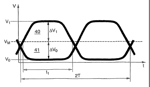
In an optical transmission signal the probability of sending a logic one
generally equals
the probability of sending a logic zero because the signal is scrambled before
transmission in order to maintain 0.5 the probability of each symbol. A signal
profile in
accordance with the invention is shown in Figure 4, in which, for the above
conditions,
the mean value VM of the signal is that for which the two areas 40, 41 are
equal.
To maintain equal the two areas when y is lower than 50%, OVl must become
greater
than OVo. If the electrical signal is biased across the decision level that
distinguishes
logical ones from logical ze'ros (which is commonly the case in AC coupled
receivers of
which that shown in Figure 2 is an example)the logical ones are moved further
away
from the threshold level VM by altering the characteristic of the transmitted
signal, and
without the need to. modify the receiver.
This way of biasing the electrical signal is auto adaptive and it is not
affected by
variation of the input optical power because the mean level of the signal does
not
change (the signal is AC coupled) and even if the peak to peak amplitude
changes the
ratio OVi/AVo is constant because it is related to the value of 7(a parameter
of the
transmitter, independent on the received power).