Note: Descriptions are shown in the official language in which they were submitted.
CA 02424702 2003-04-03
WO 02/29974 PCT/USO1/31251
SYNCHRONIZED MLJLTI-OUTPUT DIGITAL CLOCK MANAGER
FIELD OF THE INVENTION
The present invention relates to digital clocking
circuits for digital electronics. More specifically, the
present invention relates to digital clock managers capable
of generating multiple phase-locked output clock signals of
different frequencies.
BACKGROUND OF THE INVENTION
Synchronous digital systems, including board level
systems and chip level systems, rely on one or more clock
signals to synchronize elements across the system.
Typically, one or more clock signals are distributed across
the system on one or more clock lines. However, due to
various problems such as clock buffer delays, high
capacitance of heavily loaded clock lines, and propagation
delays, the edges of a clock signal in different parts of
the system may not be synchronized. The time difference
between a rising (or falling) edge in one part of the
system with the corresponding rising (or falling) edge in
another part of the system is referred to as "clock skew".
Clock skew can cause digital systems to malfunction.
For example, it is common for circuits in digital systems
to have a first flip-flop output driving a second flip-flop
input. With a synchronized clock signal on the clock input
terminal of both flip-flops, the data in the first flip-
flop is successfully clocked into the second flip-flop.
However, if the active edge on the second flip flop is
delayed by clock skew, the second flip-flop might not
capture the data from the first flip-flop before the first
flip-flop changes state.
Delay lock loops are used in digital systems to
minimize clock skew. Delay lock loops typically use delay
elements to synchronize the active edges of a reference
1
CA 02424702 2003-04-03
WO 02/29974 PCT/USO1/31251
clock signal in one part of the system with a feedback
clock signal from a second part of the system. Figure 1
shows a block diagram of a conventional delay lock loop 100
coupled to logic circuits 190. Delay lock loop 100, which
comprises a delay line 110 and a phase detector 120,
receives a reference clock signal REF_CLK and drives an
output clock signal O CLK.
Delay line 110 delays reference clock signal REF_CLK
by a variable propagation delay D before supplying output
clock signal 0_CLK. Thus, each clock edge of output clock
signal 0_CLK lags a corresponding clock edge of reference
clock signal REF CLK by propagation delay D (see Figure
2(a)). Phase detector 120 controls delay line 110, as
described below. Delay line 110 is capable of producing a
minimum propagation delay D MIN and a maximum propagation
delay D MAX.
Before output clock signal 0_CLK reaches logic
circuits 190, output clock signal 0_CLK is skewed by clock
skew 180. Clock skew 180 can be caused by delays in
various clock buffers (not shown) or propagation delays on
the clock signal line carrying output clock signal 0_CLK
(e.g., due to heavy loading on the clock signal line). To
distinguish output clock signal 0 CLK from the skewed
version of output clock signal 0_CLK, the skewed version is
referred to as skewed clock signal S_CLK. Skewed clock
signal S CLK drives the clock input terminals~(not shown)
of the clocked circuits within logic circuits 190. Skewed
clock signal S CLK is also routed back to delay lock loop
100 on a feedback path 170. Typically, feedback path 170
is dedicated specifically to routing skewed clock signal
S_CLK to delay lock loop 110. Therefore, any propagation
delay on feedback path 170 is minimal and causes only
negligible skewing.
Figure 2(a) provides a timing diagram of reference
clock signal REF~CLK, output clock signal 0 CLK, and skewed
clock signal S_CLK. All three clock signals have the same
frequency F REF (not shown) and period P_REF, and all are
active-high (i.e., the rising edge is the active edge).
2
CA 02424702 2003-04-03
WO 02/29974 PCT/USO1/31251
Since output clock signal O CLK is delayed by propagation
delay D, a clock edge 220 of output clock signal O_CLK lags
corresponding clock edge 210 of reference clock signal
REF_CLK by propagation delay D. Similarly, a clock edge
230 of skewed clock signal S_CLK lags corresponding clock
edge 220 of output clock signal 0_CLK by a propagation
delay SKEW, which is the propagation delay caused by clock
skew 180 (Figure 1). Therefore, clock edge 230 of skewed
clock signal S_CLK lags clock edge 210 of reference clock
signal REF_CLK by a propagation delay DSKEW, which is equal
to propagation delay D plus propagation delay SKEW.
Delay lock loop 100 controls propagation delay D by
controlling delay line 110. However, delay line 110 cannot
create negative delay; therefore, clock edge 230 cannot be
synchronized to clock edge 210. Fortunately, clock signals
are periodic signals. Therefore, delay lock loop 100 can
synchronize reference clock signal REF CLK and skewed clock
signal S CLK by further delaying output clock signal 0_CLK
such that clock edge 240 of skewed clock signal S_CLK is
synchronized with clock edge 210 of reference clock signal
REF_CLK. As shown in Figure 2(b), propagation delay D is
adjusted so that propagation delay DSKEW is equal to period
P. Specifically, delay line 110 is tuned so that
propagation delay D is increased until propagation delay D
equals period P minus propagation delay SKEW. Although
propagation delay DSKEW could be increased to any multiple
of period P to achieve synchronization, most delay lock
loops do not include a delay line capable of creating such
a large propagation delay.
Phase detector 120 (Figure 1) controls delay line 110
to regulate propagation delay D. The actual control
mechanism for delay lock loop 100 can differ. For example,
in one version of delay lock loop 100, delay line 110
starts with a propagation delay D equal to minimum
propagation delay D MIN, after power-on or reset. Phase
detector 110 then increases propagation delay D until
reference clock signal REF CLK is synchronized with skewed
clock signal S_CLK. In another system, delay lock loop 100
3
CA 02424702 2003-04-03
WO 02/29974 PCT/USO1/31251
starts with a propagation delay D equal to the average of
minimum propagation delay D MIN and maximum propagation
delay D MAX, after power-on or reset. Phase detector 120
then determines whether to increase or decrease (or
neither) propagation delay D to synchronize reference clock
signal REF CLK with skewed clock signal S_CLK. For example,
phase detector 120 would increase propagation delay D for
the clock signals depicted in Figure 2(a). However, phase
detector 120 would decrease propagation delay D for the
clock signals depicted in Figure 2(c).
In Figure 2(c), skewed clock signal S CLK is said to
"lag" reference clock signal REF_CLK, because the time
between a rising edge of reference clock signal REF_CLK and
the next rising edge of skewed clock signal S_CLK is less
than the time between a rising edge of skewed clock signal
S CLK and the next rising edge of reference clock signal
REF CLK. However, in Figure 2(a), reference clock signal
REF_CLK is said to "lag" skewed clock signal S_CLK, because
the time between a rising edge of skewed clock signal S_CLK
and the next rising edge of reference clock signal REF_CLK
is less than the time between a rising clock edge of
reference clock signal REF_CLK and the next rising clock
edge of skewed clock signal S_CLK. Alternatively, in
Figure 2(a) skewed clock signal S CLK could be said to
"lead" reference clock signal REF_CLK.
After synchronizing reference clock signal REF CLK and
skewed clock signal S_CLK, delay lock loop 100 monitors
reference clock signal REF_CLK and skewed clock signal
S CLK and adjusts propagation delay D to maintain
synchronization. For example, if propagation delay SKEW
increases, perhaps caused by an increase in temperature,
delay lock loop 100 must decrease propagation delay D to
compensate. Conversely, if propagation delay SKEW
decreases, perhaps caused by a decrease in temperature,
delay lock loop 100 must increase propagation delay D to
compensate. The time in which delay lock loop 100 is
attempting to first synchronize reference clock signal
REF_CLK and skewed clock signal S_CLK, is referred to as
4
CA 02424702 2003-04-03
WO 02/29974 PCT/USO1/31251
lock acquisition. The time in which delay lock loop 100 is
attempting to maintain synchronization is referred to as
lock maintenance. The value of propagation delay D at the
end of lock acquisition, i.e. when synchronization is
initially established, is referred to as initial
propagation delay ID.
Further complications with clock skew exists in
complex digital systems, such as microprocessors and FPGAs,
that have multiple clock signals at different frequencies.
For example, in some microprocessors, internal circuits are
clocked by a first clock signal at a first clock frequency
while input/output (I/O) circuits are clocked by a second
clock signal at a second clock frequency. Typically, the
second clock frequency is slower than the first clock
frequency.
Most systems use one clock generating circuit to
generate a first clock signal and a specialized circuit to
derive other clock signals from the first clock signal.
For example, clock dividers are used to generate one or
more clock signals of lower clock frequencies from a
reference clock signal. Typically, clock dividers divide
the frequency of the reference clock signal by an integer
value. Conversely, clock multipliers are used to generate
one or more clock signals of higher clock frequencies from
the reference clock signal. Combining clock multipliers
with clock dividers provide clocking circuits which can
generate one or more clock signals having frequencies that
are fractional values of the frequency of the reference
clock signal.
Thus, a clocking circuit is typically coupled to
reference clock signal REF CLK to generate a frequency
adjusted clock signal FRED CLK. However, the clocking
circuits add additional skew due to propagation delay and
gate switching times. Consequently, frequency adjusted
clock signal FREQ CLK may be skewed compared to both
reference clock signal REF CLK and output clock signal
0 CLK. Hence, there is a need for a method and circuits,
5
CA 02424702 2003-04-03
WO 02/29974 PCT/USO1/31251
that can compensate for skew in bath an output clock signal
and a frequency adjusted clock signal.
SUMMARY
The present invention provides a digital clock manager
that generates a deskewed output clock signal as well as a
deskewed frequency adjusted clock signal. Specifically,
the output clock signal causes a skewed clock signal to be
synchronized with a reference clock signal. The frequency
adjusted clock signal is synchronized with the output clock
signal during concurrences. Generally the frequency
adjusted clock signal is driven to a selected clock
frequency which is equal to the clock frequency of the
output clock signal multiplied by a multiplier M and
l5.divided by a divider D, where M and D are natural numbers.
When the frequency of the frequency adjusted clock signal
is equal to the selected frequency and the frequency
adjusted clock signal is in phase with the output clock
signal, every Mth rising edge of the frequency adjusted
clock signal aligns with a rising edge of the output clock
signal. The alignments are commonly referred to as
concurrences.
One embodiment of the digital clock manager includes a
delay lock loop (DLL) and a digital frequency synthesizer
(DFS). The delay lock loop is configured to generate an
output clock signal that synchronizes a skewed clock signal
with a reference clock signal. The delay lock loop also
generates a synchronizing clock signal, which is provided
to the digital frequency synthesizer. The delay lock loop
has a DLL output circuit that generates the output clock
signal, which lags the synchronizing clock signal by a DLL
output delay. In the digital frequency synthesizer, a DFS
output circuit generates a frequency adjusted clock signal
in which an active edge of the frequency adjusted clock
signal lags an active edge of the synchronizing clock
signal by a DFS output delay during a concurrence period.
By matching the DLL output delay with the DFS output delay,
6
CA 02424702 2003-04-03
WO 02/29974 PCT/USO1/31251
the output clock signal and the frequency adjusted clock
signals are synchronized.
The present invention will be more fully understood in
view of the following description and drawings.
BRIEF DESCRIPTION OF THE DRAWINGS
Figure 1 is a block diagram of a system using a
conventional delay lock loop.
Figures 2(a), 2(b) and 2(c) are timing diagrams for
the system of Figure 1.
Figure 3 is a block diagram of a digital clock manager
in accordance with one embodiment of the present invention.
Figure 4 is a block diagram of a digital clock manager
in accordance with one embodiment of the present invention.
Figure 5 is a block diagram of a digital clock manager
in accordance with one embodiment of the present invention.
Figure 6 is a block diagram of a system using an
embodiment of a delay lock loop in accordance with the
present invention.
Figure 7 is a timing diagram for the delay lock loop
of Figure 6.
Figure 8 illustrates a lock window as used in
accordance with one embodiment of the present invention.
Figure 9 is a block diagram of an embodiment of a
clock phase shifter in accordance with the present
invention.
Figure 10 is a block diagram of another embodiment of
a clock phase shifter in accordance with the present
invention.
Figure 11 is a block diagram of an output generator in
accordance with the present invention.
Figure 12 is a state diagram for an embodiment of a
controller in accordance with the present invention.
Figure 13 is a block diagram of a system using another
embodiment of a delay lock loop in accordance with the
present invention.
7
CA 02424702 2003-04-03
WO 02/29974 PCT/USO1/31251
Fig. 14(a) is a block diagram of a variable clocking
circuit in accordance with one embodiment of the present
invention.
Fig. 14(b) is a timing diagram for the variable
clocking circuit of Fig. 14(a).
Fig. 15 is schematic diagram of a variable digital
oscillator in accordance with one embodiment of the present
invention.
Fig. 16 is a timing diagram for the variable clocking
circuit of Fig. 14(a) using the digital oscillator of Fig.
15.
Fig. 17 is a block diagram of an oscillator control
circuit in accordance with one embodiment of the present
invention.
Fig. 18 is a block diagram of an initialization
circuit in accordance with a second embodiment of the
present invention.
Fig. 19 is a timing diagram for the variable clocking
circuit of Fig. 14(a) using a delay line fine tuning
controller.
Fig. 20 is a block diagram of a delay line fine tuning
controller in accordance with one embodiment of the present
invention.
Fig. 21 is a block diagram of a modulo-M delta sigma
circuit in accordance with one embodiment of the present
invention.
DETAILED DESCRIPTION
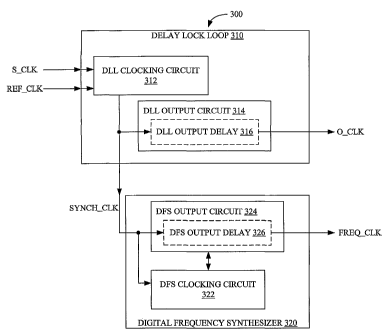
Fig. 3 is a block diagram of a digital clock manager
300 in accordance with one embodiment of the present
invention. Digital clock manager 300, which receives a
reference clocks signal REF_CLK and a skewed clock signal
S CLK, generates an output clock signal O_CLK, which causes
skewed clock signal S CLK to be synchronized with reference
clock signal REF CLK, and a frequency adjusted clock signal
FREQ CLK which is phase locked with output clock signal
O CLK during c.oncurrences. Generally, frequency adjusted
clock signal FREQ_CLK has an adjusted frequency F ADJ which
8
CA 02424702 2003-04-03
WO 02/29974 PCT/USO1/31251
is equal to the frequency of output clock signal 0_CLK
multiplied by a multiplier M and divided by a divider D.
If frequency adjusted clock signal FREQ CLK is in phase
with clock signal 0 CLK, every Mth rising edge of frequency
adjusted clock signal FREQ CLK aligns with a rising edge of
output clock signal 0 CLK. The alignments are commonly
referred to as concurrences. Reference clock signal
REF CLK and output clock signal 0 CLK have the same
frequency. For clarity, reference frequency F REF is used
to denote the frequency of both reference clock signal
REF CLK and output clock signal 0 CLK.
The embodiment of Fig. 3 includes a delay lock loop
310 and a digital frequency synthesizer 320. While
specific embodiments of delay lock loop 310 and digital
frequency synthesizer 320 are described below, the
principles of the present invention can be adapted for use
with almost any delay lock loop and any digital frequency
synthesizer. Thus, the description with respect to digital
clock manager 300 describes delay lock loop 310 and digital
frequency synthesizer 320 is in general terms. One skilled
in the art can adapt the principles of the present
invention to create a~digital clock manager with a variety
of delay lock loops and digital frequency synthesizers.
Delay Lock Loop 310 includes DLL clocking circuit 312
and DLL output circuit 314. DLL clocking circuit 312
generates a synchronizing clock signal SYNCH CLK, which is
provided to DLL output circuit 314 and DFS output circuit
324 of digital frequency synthesizer 320. Generally,
synchronizing clock signal SYNCH CLK has a frequency equal
to frequency F REF of reference clock signal REF CLK and
output clock signal 0 CLK. DLL output circuit 314 drives
output clock signal 0 CLK. DLL output circuit 314
introduces a DLL output delay 316 between synchronizing
clock signal SYNCH CLK and output clock circuit 0_CLK.
Specifically, output clock signal O_CLK lags synchronizing
clock signal SYNCH CLK by DLL output delay 316. DLL
Clocking circuit 312 and DLL output circuit 314 together
synchronizes skewed clock signal S CLK with reference clock
9
CA 02424702 2003-04-03
WO 02/29974 PCT/USO1/31251
signal REF_CLK. A specific embodiment of delay lock loop
310 used in one embodiment of the present invention is
described below.
Digital frequency synthesizer 320 receives
synchronized clock signal SYNCH_CLK and generates frequency
adjusted clock signal FREQ CLK having adjusted frequency
F ADJ, which is equal to the frequency of output clock
signal 0_CLK multiplied by a multiplier M and divided by a
divider D. As shown in Fig. 3, digital frequency
synthesizer 320 includes a DFS clocking circuit 322 and a
DFS output circuit 324. DFS output circuit 324 drives
frequency adjusted clock signal FREQ CLK and introduces a
DFS output delay 326 between frequency adjusted clock
signal FREQ CLK and synchronizing clock signal SYNCH CLK.
Specifically, during concurrence periods of synchronizing
clock signal SYNCH CLK with frequency adjusted clock signal
FREQ CLK, an active edge of frequency adjusted clock signal
FRED CLK lags an active edge of synchronizing clock signal
SYNCH CLK by DFS output delay 326. DFS clocking circuit
322 and DFS output circuit 324 combine to perform the
frequency adjustments necessary to generate frequency
adjusted clock signal FRED CLK.
Because output clock signal 0 CLK lags synchronizing
clock signal SYNCH CLK by DLL output delay 316 and
frequency adjusted clock signal FREQ_CLK lags synchronizing
clock signal SYNCH CLK by DFS output delay 326, frequency
adjusted clock signal FREQ CLK can be synchronized with
output clock signal O_CLK by matching DLL output delay 316
with DFS output delay 326. Thus, in accordance with some
embodiments of the invention, the components of DFS output
circuit 324 and DLL output circuit 314 are chosen to match
DLL output delay 316 with DFS output delay 326. For
example, in some embodiments of the present invention, DLL
output circuit 314 and DFS output circuit 324 comprise the
identical components. Furthermore, in some embodiments of
the present invention, the layout and routing for DLL
output circuit 314 closely match the layout and routing for
DFS output circuit 324. By matching components, layout,
CA 02424702 2003-04-03
WO 02/29974 PCT/USO1/31251
and routing, these embodiments of the present invention can.
achieve near-perfect matching between DLL output delay 316
and DFS output delay 326.
However, some embodiments of the present invention can
not achieve suitable matching of DFS output delay 326 and
DLL output delay 316. For these embodiments, additional
delay circuitry can be used to synchronize output clock
signal 0_CLK and frequency adjusted clock signal FRED CLK.
Fig. 4 is a block diagram of a digital clock manager 400
using variable delay circuits 410 and 420 in accordance
with one embodiment of the present invention. Because,
digital clock manager 400 is similar to digital clock
manager 300, similar reference numerals are used for
similar elements. In addition, descriptions of the
repeated elements are omitted for brevity. Variable delay
circuit 410 is coupled to DLL output circuit 314 and
generates output clock signal O CLK. Similarly, variable
delay circuit 420 is coupled to DFS output circuit 324 and
generates frequency adjusted clock signal FRED CLK.
In digital clock manager 400, DLL output delay 316 and
DFS output delay 326 can not be adequately matched.
However, variable delay circuit 410, which provides
additional delay to DLL output delay 316, and variable
delay circuit 420, which provides additional delay to DFS
output delay 326 can be used to synchronize output clock
signal 0 CLK with frequency adjusted clock signal FREQ CLK.
Specifically, DLL output delay 316 plus the delay provided
by variable delay circuit 410 should be matched with DFS
output delay 326 plus the delay provided by variable delay
circuit 420. In many embodiments of the present invention,
delay match can be achieved using only one of variable
delay circuits 410 or 420. Therefore, these embodiments
would not need to include both variable delay circuit 410
and variable delay circuit 420.
Fig. 5 is a block diagram of a digital clock manager
500 in accordance with one embodiment of the present
invention. Because, digital clock manager 500 is similar
to digital clock manager 300, similar reference numerals
11
CA 02424702 2003-04-03
WO 02/29974 PCT/USO1/31251
are used for similar elements. In addition, descriptions
of the repeated elements are omitted for brevity. Digital
clock manager 500 reduces the time required to generate
frequency adjusted clock signal FREQ CLK as compared to
digital clock manager 300. As is well known in the art,
delay lock loops operate in a lock acquisition mode prior
to generating a stable output clock signal. Similarly,
digital frequency synthesizers operate in various frequency
search phases prior to generating a stable frequency
adjusted clock signal. In digital clock manager 300, delay
lock loop 310 must first undergo a lock acquisition mode to
generate synchronizing clock signal SYNCH CLK. Then
digital frequency synthesizer must undergo various
frequency search phases prior to generating frequency
adjusted clock signal FREQ CLK.
However, in digital clock manager 500, lock
acquisition by delay lock loop 310 and frequency search
phases by digital frequency synthesizer 320 can occur
simultaneously to reduce the time necessary to generate
output clock signal O_CLK and frequency adjusted clock
signal FREQ CLK. Specifically, digital clock manager 500
includes a multiplexer 510, having a first input terminal
coupled to receive reference clock signal REF CLK, a second
input terminal coupled to receive synchronizing clock
signal SYNCH CLK and an output terminal coupled to digital
frequency synthesizer 320. Multiplexer 510 is controlled
by a clock transition control signal CLK TRAM from digital
frequency synthesizer 320. Clock transition~control signal
CLK_TRAM is driven to an inactive state while delay locked
loop is performing lock acquisition or digital frequency
synthesizer 320 is not ready for a clock transition. If
clock transition control signal is in the inactive state,
multiplexer 510 couples reference clock signal REF_CLK to
digital frequency synthesizer 320.
Because reference clock signal REF CLK is already at
reference frequency F REF, digital frequency synthesizer
320 can perform the required frequency search phases using
reference clock signal REF CLK. After delay lock loop 310
12
CA 02424702 2003-04-03
WO 02/29974 PCT/USO1/31251
finishes lock acquisition, a Control signal DLL LOCKED is
driven to an active state (e. g., logic high) signaling
digital frequency synthesizer 320 that delay lock loop 310
has completed lock acquisition. Then, when digital
frequency synthesizer is ready for transitioning to
synchronizing clock signal SYNCH CLK, clock transition
control signal CLK_TRAM is driven to the active state,
which causes synchronizing clock signal SYNCH CLK to be
provided to digital frequency synthesizer 320. For
example, in some embodiments of the present invention,
digital frequency synthesizer 320 completes a frequency
search phase prior to driving control signal CLK TRAM to
select synchronizing clock signal SYNCH CLK. Furthermore,
in some embodiments of the present invention, digital
frequency synthesizer 320 is halted prior to switching from
reference clock signal REF CLK to synchronizing clock
signal SYNCH CLK and then restarted. Thus, digital clock
manager 500 reduces the time required to generate frequency
adjusted clock signal FREQ CLK by allowing acquisition lock
by delay lock loop 310 and frequency searches by digital
frequency synthesizer 320 to operate simultaneously.
Figure 6 is a block diagram of a system using a delay
lock loop 600 in accordance with one embodiment of the
present invention. Delay lock loop 600 comprises a delay
line 610, a clock phase shifter 650, a controller 630, an
output generator 640, and a phase detector 620. Delay lock
loop 600 receives reference clock signal REF CLK on a
reference input terminal 602 and generates output clock
signal 0_CLK on output terminal 604. As explained above
with respect to Figure 1, output clock signal O CLK is
skewed by clock skew 180 into skewed clock signal S_CLK,
which clocks logic circuits 190. Skewed clock signal S CLK
is also fed back to a feedback terminal 606 of delay lock
loop 600 on feedback path 170.
Within delay lock loop 600, reference clock signal
REF_CLK is delayed by delay line 610 to generate delayed
clock signal D CLK. Delayed clock signal D CLK is delayed
from clock signal REF CLK by a propagation delay D in delay
13
CA 02424702 2003-04-03
WO 02/29974 PCT/USO1/31251
line 610. One embodiment of delay lock loop 600 uses an
adjustable delay line described in U.S. Patent Application
Serial No. 09/102,704 entitled "Glitchless Delay Line Using
Gray Code Multiplexer" by Andrew K. Percey. However, other
adjustable delay lines can also be used with delay lock
loop 600. Delayed clock signal D CLK is provided to an
input terminal of a clock phase shifter 650 and to an input
terminal of an output generator 640. Delayed clock signal
D CLK is also provided to digital frequency synthesizer 320
as synchronizing clock signal SYNCH CLK.
Clock phase shifter 650 generates one or more phase-
shifted clock signals P CLK_1 to P_CLK N-1, where N is a
positive integer. In one embodiment, phase-shifted clock
signal P_CLK_1 is phase-shifted by 360/N degrees from
delayed clock signal D CLK. Phase-shifted clock signal
P CLK_2 is phase-shifted by 2*(360/N) degrees. Phase-
shifted clock signal P CLK_N-1 is phase-shifted by
(N-1)*(360/N) degrees. Thus, in general a phase-shifted
clock signal P_CLK_z is phase-shifted by 2*(360/N), where z
is an integer between 1 and (N-1), inclusive. Delayed
clock signal D_CLK can be considered a phase-shifted clock
signal P CLK_0 since delayed clock signal D_CLK has a 0
degree phase shift from itself. Further, in some
embodiments of delay lock loop 600, clock phase shifter 650
generates a phase-shifted signal P CLK N that has the same
phase and frequency as delayed clock signal D CLK.
Thus, in an embodiment of clock phase shifter 650
where N is equal to four, phase-shifted clock signal
P_CLK_1 is phase-shifted 90 degrees from delayed clock
signal D CLK. It logically follows that phase-shifted
clock signal P CLK_2 is phase-shifted by 180 degrees from
delayed clock signal D_CLK and phase-shifted clock signal
P_CLK_3 is phase-shifted by 270 degrees from delayed clock
signal D_CLK. However, the principles of the present
invention are also suitable for other embodiments of clock
phase shifter 650 using other patterns of phase shifting
between the phase-shifted clock signals.
14
CA 02424702 2003-04-03
WO 02/29974 PCT/USO1/31251
Phase shifting is a concept in the frequency domain of
a clock signal. The equivalent of phase shifting in the
time domain is delaying the clock signal. Specifically, if
a first clock signal is phase-shifted from a second clock
signal by X degrees, the first clock signal is delayed by
X*(P/360), where P is the period of the first and second
clock signals. Thus, if phase-shifted clock signal P CLK_1
is phase-shifted 90 degrees from delayed clock signal
D CLK, phase-shifted clock signal P_CLK_1 is delayed by
one-fourth of the period of delayed clock signal D_CLK. To
distinguish delays caused by phase shifting from other
propagation delays, delays caused by phase shifting are
referred to as phase-shifted delays P D_z. Since a phase-
shifted clock signal P_CLK_Z is phase-shifted by 2*(360/N)
degrees, phase-shifted clock signal P CLK_Z has a phase-
shifted delay P D_Z equal to Z*(P/N), where Z is an integer
between 1 and (N-1), inclusive.
Figure 7 illustrates for a timing diagram for delay
lock loop 600 (Figure 6) wherein N equals 4. Specifically,
clock phase shifter 650 generates phase-shifted clock
signal P_CLK_1 90 degrees out of phase with delayed clock
signal D CLK. Thus, phase-shifted clock signal P-CLK_1 is
delayed by one-fourth of clock period P. Clock phase
shifter 650 generates phase-shifted clock signal P CLK 2
180 degrees out of phase with delayed clock signal D CLK.
Thus, phase-shifted clock signal P CLK_2 is delayed by half
of clock period P. Finally, clock phase shifter 650
generates phase-shifted clock signal P CLK_3 270 degrees
out of phase with delayed clock signal D CLK. Thus, phase-
shifted clock signal P CLK_3 is delayed by three-fourths of
clock period P.
Returning to Figure 6, clock phase shifter 650
provides the phase-shifted clock signals to various input
terminals of output generator 640. In some embodiments of
delay lock loop 600, clock phase shifter 650 can be
configured using one or more configuration signals CFG on
an optional configuration bus 660. An embodiment of clock
CA 02424702 2003-04-03
WO 02/29974 PCT/USO1/31251
phase shifter 650 that is configured by configuration
signals CFG is described below with respect to Figure 10.
Configuration signals CFG are received on configuration
terminals 608 and are routed to clock phase shifter 650 and
controller 630 by configuration bus 660. Output generator
640 selects either delayed clock signal D CLK or one of the
phase-shifted clock signals to provide as output clock
signal O_CLK as dictated by controller 630 (described
below). For embodiments of delay lock loop 600 in which
clock phase shifter 650 provides phase-shifted clock signal
P CLK N, output generator 640 can use phase-shifted ClOCk
signal P CLK N in place of delayed clock signal D CLK.
Controller 630 controls output generator 640.
Controller 630 receives phase information regarding
25 reference clock signal REF CLK and skewed clock signal
S_CLK from phase detector 620. Specifically, phase
detector 620 informs controller 630 whether propagation
delay D from delay line 610 should be increased or
decreased to achieve synchronization of skewed clock signal
S_CLK with reference clock signal REF_CLK. For embodiments
of phase detector 620 that only determine whether to
increase or decrease propagation delay D, a fitter filter
(not shown) can be used to reduce clock fitter. In one
embodiment, the fitter filter is an up/down counter (not
shown) that decrements by one if propagation delay D should
be decreased and increments by one if propagation delay D
should be increased. However, propagation delay D is not
adjusted until the up/down counter reaches 0 or some other
predetermined number. When propagation delay D is
adjusted, the up/down counter is reset to one-half the
maximum value. In other embodiments, phase detector 620
calculates the amount propagation. delay D should be
increased or decreased. During lock acquisition,
controller 630 attempts to synchronize skewed clock signal
S_CLK with reference clock signal REF_CLK so that initial
propagation delay ID of propagation delay D is within a
lock window W.
16
CA 02424702 2003-04-03
WO 02/29974 PCT/USO1/31251
Figure 8 illustrates the concepts of lock window W.
As explained above, propagation delay D must be between
minimum propagation delay D MIN and maximum propagation
delay D_MAX. Typical values for D MIN and D_MAX are 3.2
nanoseconds and 46.8 nanoseconds, respectively. During
lock acquisition, controller 630 ensures that initial
propagation delay ID of propagation delay D is within lock
window W. Specifically, when synchronization is first
established initial propagation delay ID must be between
lock window minimum W MIN and lock window maximum W MAX.
The limits on lock window W are set to guarantee that once
delay lock loop 600 completes locks acquisition, delay lock
loop 600 can maintain synchronization as long as the system
containing delay lock loop 600 operates within the design
guidelines of the system.
For example, the system containing delay lock loop 600
generally can operate in a range of operating conditions.
The range of operating conditions includes a maximum
extreme condition in which propagation delay SKEW is
maximized at a propagation delay value SKEW_MAX.
Similarly, the range of operating conditions also includes
a minimum extreme condition in which propagation delay SKEW
is minimized at a propagation delay value SKEW MIN. Thus,
the maximum change (DELTA_SKEW) in propagation delay SKEW
during operation of the system is equal to propagation
delay value SKEW MAX minus propagation delay value SKEW MIN
(i.e., DELTA SKEW = SKEW_MAX - SKEW MIN). For maximum
protection during lock maintenance, lock window minimum
W MIN can be equal to minimum propagation delay D MIN plus
DELTA SKEW. Similarly, lock window maximum W_MAX can be
equal to maximum propagation delay D_MAX minus DELTA_SKEW.
In one embodiment of the present invention, lock window
minimum W_MIN is equal to approximately 16.5% of maximum
propagation delay D MAX and lock window maximum W_MAX is
equal to approximately 67.8% of maximum propagation delay
D MAX.
As explained above with respect to Figure 1, for a
conventional delay lock loop synchronization of skewed
17
CA 02424702 2003-04-03
WO 02/29974 PCT/USO1/31251
clock signal S CLK with reference clock signal REF CLK is
achieved when propagation delay D plus propagation delay
SKEW is equal to a multiple of period P. In equation form:
D + SKEW = MULT(P) (1)
where MULT(P) refers to a multiple of P. Usually, the
smallest multiple of P greater than SKEW is used.
With delay lock loop 600, controller 630 can also use
the delays from the phase-shifted clock signals. Thus
delay lock loop 600 can achieve synchronization if
propagation delay D plus a phase-shifted delay P D from a
phase-shifted clock signal plus propagation delay SKEW is a
multiple of period P. In equation form:
D + P D_Z + SKEW = MULT(P) (2)
where P_D_z refers to a phase-shifted delay from phase-
shifted clock signal P CLK_z. Usually, the smallest
multiple of P greater than propagation delay SKEW plus
phase-shifted delay P_D_z is used. As explained above with
respect to Figure 6, in one embodiment of clock phase
shifter 650 phase-shifted delay P D_Z of a phase-shifted
clock signal P CLK_Z is equal to 2*(P/N), where Z is an
integer between 0 and (N-1), inclusive. If z is equal to
0, controller 630 causes output generator 640 to use
delayed clock signal D_CLK as output clock signal 0 CLK.
Thus, phase-shifted delay P D_0 is equal to 0.
For clarity, initial delay ID can be referred to
initial delay ID_0 if output generator 640 uses delayed
clock signal D CLK for output Clock signal 0 CLK.
Similarly, initial delay ID can be referred to as initial
delay ID_z, if output generator 640 uses phase-shifted
clock signal P CLK_Z for output clock signal O CLK, where Z
is a positive integer between 1 and (N-1), inclusive.
Thus, at the end of lock acquisition, equation (2) can be
rewritten as:
18
CA 02424702 2003-04-03
WO 02/29974 PCT/USO1/31251
ID_Z + P D_Z + SKEW = MULT(P) (3)
Re-arranging equation (3) provides:
ID_Z = MULT(P) - SKEW - P D_Z (4)
and substituting Z*(P/N) for P D_Z provides:
ID_Z = MULT(P) - SKEW - Z*(P/N) (5)
Usually, the smallest multiple of P that results in a
positive initial delay ID_Z is used. In situations where
initial delay ID_Z is less than minimum propagation delay
D_MIN or greater than maximum propagation delay D MAX,
delay lock loop 600 cannot synchronize skewed clock signal
S_CLK with reference clock signal REF CLK using phase-
shifted clock signal P CLK_Z.
Because controller 630 can select any one of phase-
shifted clock signals P CLK_Z to drive output clock signal
0_CLK, controller 630 can select from N initial delay
values. The possible initial delay values range from a
minimum offset value (MULT(P)-SKEW) to a maximum value
(MULT(P)-SKEW) & (N-1)/N period P). The difference between
each initial delay value is period P divided by N. For
example, if N equals four, period P equals 40 nanoseconds,
and propagation delay SKEW equals 25 nanoseconds; then
initial delays ID_0, ID_1, ID 2, and ID_3 equal 15
nanoseconds, 5 nanoseconds, 35 nanoseconds, and 25
nanoseconds, respectively (as calculated using equation
(5)). If N equals four, period P equals 40 nanoseconds,
and propagation delay SKEW equals 55 nanoseconds; then
initial delays ID_0, ID_1, ID_2, and ID_3 equal 25
nanoseconds, 15 nanoseconds, 5 nanoseconds, and 35
nanoseconds, respectively. Thus, controller 630 is likely
to find one or more initial delay values within lock window
W. If more than one initial delay value is within lock
window W, controller 630 can select any one of the initial
delay values within lock window W.
19
CA 02424702 2003-04-03
WO 02/29974 PCT/USO1/31251
Some embodiments of controller 630 can perform the
calculations described above to determine which phase-
shifted clock signal P_CLK_Z to use. However, other
embodiments use trial and error to determine which phase-
s shifted clock signal P CLK_Z to use. An embodiment of
controller 630 that uses trial and error is described below
with. respect to Figure 12.
Figure 9 illustrates one embodiment of clock phase
shifter 650 of Figure 6. The embodiment of clock phase
shifter 650 in Figure 9 comprises a phase detector 920 and
a plurality of delay lines 910_1 to 910 N. Delay lines
910_1 to 910 N are coupled in series. The input terminal
of delay line 910_1 receives an input clock signal such as
delayed clock signal D CLK (Figure 6). The output terminal
of delay line 910 N is coupled to an input terminal of
phase detector 920. Phase detector 920 also receives input
clock signal D CLK on another input terminal. Phase
detector 920 controls all the delay lines in parallel via
control line 925, and each delay line provides the same
amount of propagation delay. Consequently, input clock
signal D CLK and the clock signal P_CLK-N on the output
terminal of delay line 910 N are synchronized, i.e., in
phase. Further, phase detector 920 causes the total
propagation delay generated by delay lines 910-1 to 910 N
to be equal to one period P of the input clock. Thus, each
delay line provides a propagation delay of P/N. Thus, the
output terminal of delay line 910_1 provides a clock signal
that is delayed from the input clock signal by P/N whereas
the output terminal of delay line 910 2 provides a clock
signal that is delayed from the input clock signal by
2*P/N. In general, the output terminal of delay line 910 Z
provides a clock signal that is delayed from the input
clock signal by z*P/N, where z is an integer between 1 and
N-1, inclusive. Accordingly, if the input clock signal is
delayed clock signal D CLK, the output terminals of delay
lines 910_1 to 910 N-1 provide phase-shifted clock signals
P CLK_1 to P_CLK N-1, respectively. Some embodiments of
clock phase shifter 650 also generate a clock signal
CA 02424702 2003-04-03
WO 02/29974 PCT/USO1/31251
P_CLK-N on the output terminal of delay line 910 N that has
the same phase as delayed clock signal D_CLK.
Figure 10 shows a configurable embodiment of clock
phase shifter 650 of Figure 6. Specifically, the clock
phase shifter of Figure 10 can be configured in a first ,
mode to produce three phase-shifted clock signals that are
90 degrees, 180 degrees, and 270 degrees out of phase with
an input clock signal. In a second mode, the clock phase
shifter of Figure 10 produces a single phase-shifted clock
signal that is 180 degrees out of phase with the input
clock signal. The clock phase shifter of Figure 10
comprises a phase detector 1020, delay lines 1010_1,
1010 2, 1010_3, and 1010_4, and multiplexers 1030_1,
1030 2, 1030 3, and 1030 4. A configuration line 1040 is
coupled to the select terminal of multiplexers 1030_1 to
1030 4.
The input terminal of delay line 1010_1 is coupled to
receive an input clock signal such as delayed clock signal
D CLK (Figure 6). The output terminal of each delay line
1010_Z is coupled to the logic one input terminal of
multiplexes 1030_Z, where 2 is an integer between 1 and 4,
inclusive. The output terminal of each multiplexes 1030_Z
is coupled to the input terminal of delay line 2010_Z+1,
where z is an integer between 1 and 3, inclusive. The
output terminal of multiplexes 1030_4 is coupled to an
input terminal of phase detector 1020. The logic zero
input terminals of multiplexes 1030_1 and multiplexes
1030 3 are coupled to ground. However, the logic zero
input terminal of multiplexes 1030_2 is coupled to the
output terminal of delay line 1010_1. Similarly, the logic
zero input terminal of multiplexes 1030_4 is coupled to the
output terminal of delay line 1010 3. Phase detector 1020
also receives input clock signal D CLK on another input
terminal. Phase detector 1020 controls delay lines 1010_1
to 1010_4 in parallel as described above with respect to
phase detector 920.
If configuration line 1040 is pulled to logic one,
which puts the embodiment of Figure 10 into the first mode,
21
CA 02424702 2003-04-03
WO 02/29974 PCT/USO1/31251
delay lines 1010_1 to 1010_4 are coupled in series. In the
first mode, each delay line provides a delay of P/4. Thus,
if the input clock signal is delayed clock signal D CLK,
the output terminal of each multiplexer 1030_Z can provide
phase-shifted clock signals P CLK_1, P CLK_2, and P CLK_3.
However, if configuration line 1040 is pulled to logic
zero, which puts the embodiment of Figure 10 into the
second mode, only delay line 1010_1 and delay line 1010 3
are coupled in series. Delay lines 1010 2 and 1010 4 have
their input terminal coupled to ground through multiplexers
1030_1 and 1030_3, respectively. In the second mode delay
line 1010_1 and 1010 3 each provide a delay of P/2.
Coupling the input terminals of delay lines 1010 2 and
1010_4 to ground reduces power consumption and switching
noise. However, in the second mode the embodiment of
Figure 10 produces only one output clock signal, which is
180 degrees out of phase with the input clock signal and is
generated at the output terminal of multiplexer 1030 2.
Figure 11 shows one embodiment of output generator 640
of Figurey6. The output generator of Figure 11 comprises
an. N-input multiplexer 1110. N-input multiplexer 1110 has
N input terminals, referenced as 1110_0 to 1110 N-1, select
terminals 1112, and an output terminal 1114. When the
embodiment of output generator 640 of Figure 11 is used in
delay lock loop 600 of Figure 6, select terminals 1112 are
coupled to controller 630, input terminal 1110_0 is coupled
to receive delayed clock signal D_CLK, output terminal 1114
provides output clock signal O_CLK, and input terminals
1110_1 to 1110 N-1 are coupled to receive phase-shifted
clock signals P CLK_1 to P_CLK_N-1, respectively. Select
signals on select terminals 1112 determine which input
signal is provided on output terminal 1114. Other
embodiments of output generator 640 may include additional
circuitry, such as clock buffers and clock dividers. In
addition, some embodiments of output generator 640 drive
additional clock signals, such as various versions of the
phase-shifted clock signals.
22
CA 02424702 2003-04-03
WO 02/29974 PCT/USO1/31251
Figure 12 shows a state diagram 1200 for one
embodiment of controller 630 of Figure 6. On power-up or
reset, controller 630 transitions to a reset stage 1210.
In reset stage 1210, controller 630 sets a phase counter
(not shown) to zero, which causes output generator 640 to
provide delayed clock signal D CLK as output clock signal
0_CLK, and adjusts propagation delay D of delay line 610
(Figure 6) to a starting delay value. Starting delay
values for propagation delay D include, for example,
minimum propagation delay D_MIN, maximum propagation delay
D_MAX, or the average of minimum propagation delay D MIN
anal maximum propagation delay D MAX. Controller 1210 then
transitions to lock acquisition stage 1220.
In lock acquisition stage 1220, controller 630
synchronizes reference clock signal REF_CLK and skewed
clock signal S_CLK. Specifically, controller 630 adjusts
propagation delay D of delay line 610 based on signals from
phase detector 620. Phase detector 620 determines whether
propagation delay D must be increased or decreased to
synchronize skewed clock signal S_CLK with reference clock
signal REF CLK. Lock acquisition is described above in
greater detail with respect to Figures 6-9; therefore, the
description is not repeated. In some embodiments, clock
phase shifter 650 is also reset by the power-on/reset
signal. For some of these embodiments, controller 630 does
not adjust propagation delay D until after clock phase
shifter 650 produces phase-shifted clock signals P CLK_1 to
P_CLK_N-1. If controller 630 cannot synchronize skewed
clock signal S CLK with reference clock signal REF_CLK,
controller 630 transitions to increment phase stage 1250,
described below. Otherwise, controller 630 transitions to
check lock window stage 1230 after controller 630
synchronizes skewed clock signal S_CLK with reference clock
signal REF CLK (with an initial propagation delay ID in
delay line 610).
In check lock window stage 1230, controller 630 must
determine whether initial propagation delay ID is within
lock window W. Specifically, propagation delay ID is
23
CA 02424702 2003-04-03
WO 02/29974 PCT/USO1/31251
within lock window W if propagation delay ID is greater
than lock window minimum W MIN and less than lock window
maximum W MAX. If initial propagation delay ID is not
within lock window W, controller 630 transitions to
increment phase stage 1250. Otherwise, controller 630
transitions to lock maintenance stage 1240.
In lock maintenance stage 1240, controller 630 adjust
propagation delay D of delay line 610 to maintain
synchronization of skewed clock signal S_CLK with reference
clock signal REF CLK. Lock maintenance is described above
in greater detail; therefore, the description is not
repeated. As described above, the present invention can
maintain lock throughout the systems environment
conditions. Therefore, controller 630 remains in lock
maintenance stage 1240 unless a reset occurs that causes
controller 630 to transition to reset stage 1210.
In increment phase stage 1250, controller 630
increments the phase counter, which causes output generator
640 to select a different phase-shifted clock signal.
Further, controller 630 resets delay line 610 so that
propagation delay D returns to the starting delay value
used in reset stage 1210. Controller 630 then transitions
to lock acquisition stage 1220 and proceeds as described
above.
Figure 13 is a block diagram of another embodiment of
delay lock loop 600. The embodiment of Figure 13 uses the
same principles as described above with. respect to the
embodiment of Figure 6. However, in the embodiment of
Figure 13, clock phase shifter 650 generates phase-shifted
clock signals P CLK_1 to P CLK N-1 using reference clock
signal REF CLK. Reference clock signal REF CLK and phase-
shifted clock signals P_CLK_1 to P CLK N-1 are coupled to
an input selector 1340. Input selector 1340 selects either
reference clock signal REF CLK or one of phase-shifted
clock signals P CLK_1 to P_CLK N-1 as a delay line input
clock signal DLI CLK, which is provided to the input
terminal of delay line 610. Delay line 610 drives output
clock signal O CLK. A controller 1330 controls input
24
CA 02424702 2003-04-03
WO 02/29974 PCT/USO1/31251
selector 1340 and delay line 610 based on the phase
information provided by phase detector 620 so that delay
line 610 provides a propagation delay D that synchronizes
skewed clock signal S_CLK with reference clock signal
REF CLK. Input selector 1340 can be implemented using the
same circuit design as output generator 640.
Fig. 14(a) is a block diagram of a digital frequency
synthesizer 1400 in accordance with one embodiment of the
present invention. Digital frequency synthesizer 1400
generates a frequency adjusted clock signal FREQ CLK having
a clock frequency F ADJ equal to a clock frequency F_SYNCH
of a synchronizing clock signal SYNCH_CLK multiplied by a
multiplier M and divided by a divider D (i.e.,
F ADJ=M*F_SYNCH/D). As explained above, when digital
frequency synthesizer 320 is used with digital clock
manager 300, 400, or 500, clock frequency F_SYNCH of
synchronizing clock signal SYNCH CLK is equal to clock
frequency F REF of reference clock signal REF CLK. Digital
frequency synthesizer 1400 comprises clock dividers 1410
and 1420, optional clock selector 1430, phase comparator
1440, halt/restart circuit 1445, initialization circuit
1450, oscillator control circuit 1460, and variable digital
oscillator 1470. Clock divider 1410 receives frequency
adjusted clock signal FREQ CLK, which is generated by
variable digital oscillator 1470, and generates feedback
clock signal FBK_CLK having a frequency F FBK equal to
frequency F ADJ of output clock FRED CLK divided by
multiplier M. Clock divider 1410 drives feedback clock
signal FBK_CLK to initialization circuit 1450 and phase
comparator 1440. Clock divider 1420 receives synchronizing
clock signal SYNCH CLK and generates divided synchronizing
clock signal D SYNCH CLK having a frequency F D_SYNCH equal
to frequency F_SYNCH of synchronizing clock signal
SYNCH_CLK divided by divider D. Clock divider 1420 drives
divided synchronizing clock signal D_SYNCH CLK to
initialization circuit 1450 and phase comparator 1440.
Clock selector 1430 receives both synchronizing clock
signal SYNCH_CLK and frequency adjusted clock signal
CA 02424702 2003-04-03
WO 02/29974 PCT/USO1/31251
FREQ CLK and selectively drives either synchronizing clock
signal SYNCH CLK or frequency adjusted clock signal
FREQ CLK as control clock signal CTRL CLK to initialization
circuit 1450 and oscillator control circuit 1460.
Generally, synchronizing clock signal SYNCH_CLK is used
during a coarse frequency search phase. Then, frequency
adjusted clock signal FREQ CLK is used for a fine frequency
search phase as well as during a clock maintenance phase,
i.e., maintaining the frequency of frequency adjusted clock
signal FREQ CLK at the selected frequency. The coarse
frequency search phase, the fine frequency search phase,
and the maintenance phase for one embodiment of the present
invention is described in detail below. Halt/restart
circuit 1445, which is used during coarse frequency search
phase and the fine frequency search phase, is described
below.
At power-on or reset,, initialization circuit 1450
controls oscillator control circuit 1460 to tune variable
digital oscillator 1470 to generate frequency adjusted
clock signal FREQ CLK. Specifically, initialization
circuit 1450 tunes variable digital oscillator 1470 so that
frequency F ADJ of frequency adjusted clock signal FREQ CLK
is equal to a selected frequency F SEL, which equals
frequency F_SYNCH of synchronizing clock signal SYNCH CLK
multiplied by multiplier M and divided by divider D. After
frequency F_ADJ of frequency adjusted clock signal FREQ CLK
reaches selected clock frequency F SEL, initialization
circuit 1450 passes control of oscillator control circuit
1460 and variable digital oscillator 1470 to phase
comparator 1440. Phase comparator 1440 tunes variable
digital oscillator 1470 to maintain frequency F ADJ at
selected frequency F_SEL despite environmental changes such
as temperature.
Some embodiments of digital frequency synthesizer 1400
can use conventional clock dividers, clock selectors,
halt/restart circuits, and phase comparators. However,
detailed descriptions of specific embodiments of
initialization circuits 1450, oscillator control circuit
26
CA 02424702 2003-04-03
WO 02/29974 PCT/USO1/31251
1460, and variable digital oscillator 1470 are described
below.
Fig. 14(b) is a timing diagram for digital frequency
synthesizer 1400. For clarity, Fig 14(b) is idealized and
omit such factors as propagation delay and skewing. In
Fig. 14(b), multiplier M is equal to 7 and divider D is
equal to 5. Thus, as shown in Fig. 14(b), divided
synchronizing clock signal D_SYNCH CLK has a rising edge,
such as rising edges 1421, 1423, and 1425, at every fifth
rising edge of synchronizing clock signal SYNCH CLK, i.e.,
at rising edges 1401, 1403, and 1405. Similarly, feedback
clock signal FBK_CLK has a rising edge, such as rising
edges 1411, 1413, and 1415, every seventh rising edge of
frequency adjusted clock signal FREQ_CLK, i.e., at rising
edges 1471, 1473 and 1475. When frequency F ADJ of
frequency adjusted clock signal FREQ_CLK is equal to
selected frequency F SEL and synchronizing clock signal
SYNCH CLK is in phase with frequency adjusted clock signal
FREQ CLK, feedback clock signal FBK_CLK and divided
synchronizing clock signal D_SYNCH CLK have the same phase
and frequency. Accordingly, initialization circuit 1450
and phase comparator 1440 tune variable digital oscillator
1470 to match the phase and frequency of divided
synchronizing clock signal D SYNCH_CLK and feedback clock
signal FBK_CLK to drive frequency adjusted clock signal
FREQ_CLK at selected frequency F_SEL. When the phase and
frequency of divided synchronizing clock signal D_SYNCH_CLK
and feedback clock signal FBCK_CLK match, every Mth rising
edge of frequency adjusted clock signal FREQ_CLK aligns
with a rising edge of synchronizing clock signal SYNCH CLK.
For example, rising edges 1471 and 1473 of frequency
adjusted clock signal FREQ CLK align with rising edges 1401
and 1403 of synchronizing clock signal SYNCH_CLK. The
alignments are commonly referred to as concurrences. The
time between two consecutive concurrences is commonly
referred to as a concurrence period.
Fig. 15 is a block diagram of an embodiment of
variable digital oscillator 1470. The embodiment of Fig.3
27
CA 02424702 2003-04-03
WO 02/29974 PCT/USO1/31251
comprises a dual-input edge-triggered SR circuit 1510, an
inverter 1540, and a variable delay line 1520 having a low
precision delay line 1525 and a trim circuit 1527. Dual-
input edge-triggered SR circuit 1520 includes a first set
input terminal S_IN1, a first set enable input terminal
S EN1, a second set input terminal S_IN2, a second set
enable input S EN2, a first reset input terminal R_IN1, a
first reset enable input terminal R_EN1, a second reset
input terminal R_IN2, a second reset enable input terminal
R EN2, and an output terminal OUT. Operation and
construction of dual-input edge-triggered SR circuits are
well known in the art and therefore are not described in
detail herein. Table 1 provides a truth table for an
active high version of dual-input edge-triggered SR
CIRCUIT 1510. Basically, an active (e.g., rising) edge of
a set input signal on a set terminal while the
corresponding set enable signal at the set enable terminal
is at an enabled logic level (e. g., logic high) causes
output terminal OUT to drive an output signal to an active
state (e. g., logic high). Conversely, an active (e. g.,
rising) edge on a reset input signal on a reset terminal
while the corresponding reset enable signal on the
corresponding reset enable terminal is at an enabled logic
level (e.g., logic high) causes output terminal OUT to
drive an output signal to an inactive state (e. g., logic
low). For clarity, the circuits herein are described using
logic high as the enabled logic level and the active logic
level. Similarly, rising edges are used as the active
edges. However, those skilled in the art can apply the
principles of the present invention using different enabled
logic levels, active logic levels, and active edges.
28
CA 02424702 2003-04-03
WO 02/29974 PCT/USO1/31251
TABLE 1
S_IN1 S_ EN1 S_IN2 S_EN2 R IN1 R EN1 OUT
RE H X X X X H
X X RE H X X H
X X X X RE H L
where RE is rising H is logic high, L is logic low,
a edge,
and X is a do not care condition.
Synchronizing clock signal SYNCH CLK is coupled to
first set input terminal S_INl and a reference clock enable
signal R CLR-EN is coupled to first enable input terminal
S_EN1. Output terminal OUT of dual edge-triggered SR
CIRCUIT 1510 drives frequency adjusted clock signal
FREQ_CLK and is coupled to variable delay line 1520. In
the embodiment of Fig. 15, variable delay line 1520 is
implemented using a low precision delay line 1525 have a
base delay BD and a trim circuit 1527 that provides a delay
of 0, 0.25, 0.50, or 0.75 times base delay BD. Other
embodiments of the present invention can use conventional
variable delay lines. Variable delay line 1520 delays the
output signal of dual-input edge-triggered SR circuit 1510
by a variable amount under the control of oscillator
control circuit 2460 to generate delayed output signal
D_OUT. Delayed. output signal D OUT is coupled to first
reset input signal R IN1 as well as the input terminal of
inverter 1540. The output terminal of inverter 1540 is
coupled to second set input terminal S_IN2. An oscillator
enable signal OSC EN is coupled to second set enable
terminal S EN2. Under normal operations, oscillator enable
signal OSC EN is in the logic high state to enable variable
digital oscillator 1470. Therefore, a rising edge from
output terminal OUT that is delayed by variable delay line
1520 causes dual-input edge-triggered SR circuit 1510 to
transition to logic low. Conversely, a falling edge from
output terminal OUT that is delayed by variable delay line
1520 and inverted by inverter 1540 causes dual-input edge-
triggered SR circuit 1510 to transition to logic high.
Thus, variable digital oscillator 1470 generates a clock
signal such as frequency adjusted clock signal FREQ CLK.
29
CA 02424702 2003-04-03
WO 02/29974 PCT/USO1/31251
The frequency of frequency adjusted clock signal FREQ CLK
is controlled by the amount of delay provided by variable
delay line 1520.
In the embodiment of Fig. 15, low precision variable
delay line 1525 provides a variable delay ranging from 0 to
127 times low precision base delay LBD, where low precision
base delay LBD is the smallest non-zero delay provided by
low precision variable delay 1525. Furthermore, trim
circuit 1530 provides an additional delay of 0, 0.25, 0.5
or 0.75 base delay units. Thus, in the embodiment of Fig.
15, variable delay line 1520 can provide 512 delay values
'ranging from 0 to 127.75 low precision base delay LBD in
multiples of 0.25 low precision base delay LBD. Thus, in
the embodiment of Fig. 15, variable delay line 1520
provides a delay between 0 and 511 times a base delay BD,
which is equal to 0.25 times low precision base delay LBD.
Depending on the frequency F_SYNCH of synchronizing
clock signal SYNCH CLK, multiplier M, and divisor D,
variable delay line 1520 may not be able to provide the
exact amount of delay necessary to generate frequency
adjusted clock signal FREQ CLK at selected frequency F SEL.
Fig. 16 illustrates this problem of using digital delay
lines in clock generation circuits. Specifically, Fig. 16
shows a synchronizing clock signal SYNCH_CLK, a
conventional frequency adjusted clock signal C FREQ CLK,
and an frequency adjusted clock signal FREQ CLK generated
using a dual-input edge-triggered SR circuit 1510 in
accordance with one embodiment of the present invention.
In Fig. 16, rising edges 1651, 1661, and 1671 of
synchronizing clock signal SYNCH CLK, conventional
frequency adjusted clock signal C_FREQ_CLK, and frequency
adjusted clock signal FREQ CLK, respectively, are
synchronized.
In Fig. 16, multiplier M.is equal to 4 and divider D
is equal to 1. Synchronizing clock signal SYNCH_CLK has a
period of 50 nanoseconds. Accordingly, 25 nanoseconds
separates each consecutive clock edge in synchronizing
clock signal SYNCH CLK. Ideally, variable delay line 1520
CA 02424702 2003-04-03
WO 02/29974 PCT/USO1/31251
would provide a delay of 6.25 nanoseconds, which is equal
to 25 divided by 4. However, if the base delay unit of
variable delay line 1520 (Fig. 15) is one nanosecond, then
variable delay line 1520 is configured to provide 6
nanoseconds of delay between consecutive edges of frequency
adjusted clock signal FREQ_CLK1. As explained above,
during concurrence, i.e., every 4 periods, the rising edge
of conventional frequency adjusted clock signal C FREQ CLK
should occur at the same time as the rising edge of
synchronizing clock signal SYNCH_CLK. However, as
illustrated in Fig. 16, rising edge 1665 of conventional
output clock C FREQ CLK precedes rising edge 1655 of
synchronizing clock signal SYNCH CLK by 2 nanoseconds. The
two nanosecond misalignment reoccurs every concurrence
period. Thus, over time the misalignment can cause serious
synchronization problems in digital systems.
To eliminate the misalignment, just prior to
concurrence, i.e., when a rising edge of synchronizing
clock signal SYNCH CLK should be aligned with a rising edge
of frequency adjusted clock signal FREQ CLK, oscillator
enable signal OSC EN is deasserted and reference clock
enable signal is asserted. Thus, during a concurrence the
rising edge of synchronizing clock signal SYNCH CLK on
input terminal S_IN1 of dual-input edge-triggered SR
circuit 1510 causes a rising edge on output terminal OUT of
dual-input edge-triggered SR circuit 1510, which drives
frequency adjusted clock signal FREQ CLK. After
concurrence, oscillator enable signal OSC_EN is reasserted
and reference clock enable signal R CLK_EN is deasserted.
Thus, every Mth clock period of frequency adjusted clock
signal FREQ_CLK, frequency adjusted clock signal FREQ CLK
is realigned with synchronizing clock signal SYNCH CLK even
if variable delay line 1520 does not provide the exact
delay necessary to drive frequency adjusted ClOCk signal
FREQ-CLK at selected frequency F SEL.
Accordingly, as shown in Fig. 16, rising edge 1675 of
frequency adjusted clock signal FREQ_CLK is aligned with
rising edge 1655 of synchronizing clock signal SYNCH_CLK.
31
CA 02424702 2003-04-03
WO 02/29974 PCT/USO1/31251
Therefore, the time between falling edge 1671 of frequency
adjusted clock signal FREQ CLK and rising edge 1675 of
frequency adjusted clock signal FREQ CLK is 8 nanoseconds
rather than 6 nanoseconds. Thus, the time period during a
concurrence cycle of frequency adjusted clock signal
FREQ CLK is equal to 50 nanoseconds rather than 48
nanoseconds as would be dictated by using only variable
delay line 1520 to control the clock edges of frequency
adjusted clock signal FREQ CLK. Consequently, the
average frequency of frequency adjusted clock signal
FREQ_CLK over an concurrence period is equal to selected
frequency F_SEL.
Fig. 17 is a block diagram of oscillator control
circuit 1460 in accordance with one embodiment of the
present invention. The embodiment of Fig. 17 includes a
delay line register 1710, an optional incrementer 1730, an
optional delay line fine tuning controller 1720, and an
optional OR gate 1740. Delay line register 1710 receives a
delay value DV[8:0] from initialization circuit 1450 (Fig.
14). The contents of delay line register 1710 are provided
to incrementer 1730 and initialization circuit 1450 as
delay value feedback signals DV_FB[8:0]. Initialization
circuit 1450 adjusts delay value DV[8:0] during the coarse
frequency search phase to match frequency F ADJ of
frequency adjusted clock signal FRED CLK with selected
frequency F_SEL as described below. Delay line register
1710 also receives a carry signal CARRY and a borrow signal
BORROW from delay line fine tuning controller 1720. IF
delay line fine tuning controller 1720 is enabled, delay
line register 1710 is configured to increment when carry
signal CARRY is in the active logic level (e. g., logic
high) and to decrement on when borrow signal BORROW is in
the active logic level (e.g., logic high). Generation of
carry signal CARRY and borrow signal BORROW is described
below.
The delay value in delay line register 1710 is
selectively incremented by incrementer 1730 to generate
delay select signals DELAY SEL[8:0], which are coupled to
32
CA 02424702 2003-04-03
WO 02/29974 PCT/USO1/31251
variable delay line 1520 (Fig. 15). Specifically, delay
line fine tuning controller 1720 drives a fine tuning
increment control signal FT_INC to incrementer 1730. If
fine tuning increment control signal FT_INC is at an active
logic level (e. g., logic high), then incrementer 1730
increments the value from delay line register 1710. Delay
line fine tuning controller 1720 is controlled by frequency
comparator 1450 using control signal A/!S or by phase
comparator 1440 (Fig. 14(a)) using phase comparator control
signal PC CTRL. For the embodiment of Fig. 17, if delay
line fine tuning controller 1720 is enabled then if either
control signal A/!S or phase comparator signal PC CTRL is
in the active state (i.e., logic high) then delay line fine
tuning controller 1720 is configured to add additional
delay during a concurrence period. Thus, OR gate 1740
generates add delay signal ADD DELAY from control signal
A/!S and phase comparator control signal PC_CTRL. The use
of delay line fine tuning controller 1720 is described in
detail below.
Fig. 18 is a block diagram of initialization circuit
1450 in accordance with one embodiment of the present
invention. Initialization circuit 1450 performs a coarse
frequency search to set the value in variable delay line
1520. Specifically, during the coarse frequency search
phase, the embodiment of Fig. 18 performs a fast binary
search to determine delay value DV[8:0] for delay line
register 1710, which causes frequency F_FBK of feedback
clock FBK_CLK and frequency F D SYNCH of divided reference
clock D SYNCH CLK to be equal. Other embodiments of
initialization circuit 1450 may use other methods to select
delay value DV[8:0] for delay line register 1710. The
embodiment of Fig. 18 comprises a right shift register
1830, an adder/subtracter 1840, a frequency comparator
1850, and an overflow register 1860. .
Initially, adder/subtracter 1840 is configured to
provide a delay value DV[8:0] that causes variable delay
line 1520 to provide 50% of the maximum delay that can be
provided by variable delay line 1520. For the embodiment
33
CA 02424702 2003-04-03
WO 02/29974 PCT/USO1/31251
of Fig. 15, delay value DV[8:0] is initially set at 256,
i.e., halfway between 0 and 511. Right shift register 1830
is initially configured to be equal to half of the initial
value of delay value DV[8:0]. Thus, for the embodiment of
Fig. 15, right shifter 1830 is configured with an initial
value of 128. Adder/subtracter 1840 is controlled by
frequency~comparator 1850 to either add the value in right
shifter 1830 to the value in delay line register 1710 (Fig.
17) or to subtract the value in right shifter 1830 to the
value in delay line register 1710. Specifically, the value
in delay line register 1710 is provided by delay value
feedback signals DV_FB[8:0]. After each addition or
subtraction operation, the content of right shifter 1830 is
"right shifted", which effectively divides the value in
right shifter 1830 in half. However, right shifter 1830
maintains a minimum value of 1.
Frequency comparator 1850 receives feedback clock
signal FBK_CLK and divided reference signal D_SYNCH CLK and
generates a control signal A/!S which dictates whether
adder/subtracter 1840 performs an ADD operation or a
SUBTRACT operation. Specifically, if frequency F_FBK of
feedback clock signal FBK_CLK is greater than frequency
F D_SYNCH of divided synchronizing clock signal
D_SYNCH CLK, the delay provided by variable delay line
should be increased. Accordingly, frequency comparator
1850 causes adder/subtracter 1840 to perform an ADD
operation by driving control signal A/!S to the add logic
level (typically logic high). Conversely, if frequency
F FBK of feedback clock signal FBK_CLK is less than
frequency F_D_SYNCH of divided synchronizing clock signal
D_SYNCH CLK, the delay provided by variable delay line
should be decreased. Accordingly, frequency comparator
1850 causes adder/subtracter 1840 to perform a SUBTRACT
operation by driving control signal A/!S to the subtract
logic level (typically logic low). After each addition or
subtraction, halt/restart circuit 1445 (Fig. 14) halts and
restarts initialization circuit 1450, and oscillator
control circuit 1460 so that frequency adjusted clock
34
CA 02424702 2003-04-03
WO 02/29974 PCT/USO1/31251
signal FREQ CLK is started in phase with synchronizing
clock signal SYNCH CLK. Halting and restarting allows
frequency comparator 1850 to determine the proper value of
control signal A/!S without having to compensate for phase
variations. However, some embodiments of the present
invention may use frequency comparators that automatically
compensate for phase variations. For these embodiments,
halting and restarting may not be necessary.
In some embodiments of the present invention,
frequency comparator 1850 also generates a frequency
comparator reversal signal FC_REV. Frequency comparator
reversal signal FC_REV is driven to a active state (e. g.,
logic high) when frequency F FBK of feedback clock signal
FBK_CLK becomes greater than frequency F-D_SYNCH of divided
synchronizing clock signal D_SYNCH CLK and also when
frequency F_D_SYNCH of divided synchronizing clock signal
D_SYNCH CLK becomes greater than frequency F FBK of
feedback clock signal FBK_CLK. In one embodiment of the
present invention, a coarse frequency search phase ends
when the value of right shifter 1830 is equal to one.
Table 2 provides an example of the operation for the
embodiment of initialization circuit 1450 in Fig. 18. In
the example of Table 2, a delay value DV of 371.5 provides
the optimum delay for matching frequency F_FBK of feedback
clock signal FBK CLK to frequency F D_SYNCH of divided
synchronizing clock signal D SYNCH CLK.
CA 02424702 2003-04-03
WO 02/29974 PCT/USO1/31251
TABLE 2
Coarse
Frequency Right Shifter Delay Line
Search Step 1830 Register 1730 A !S
0 128 256 1
1 64 384 0
2 32 320 1
3 16 352 1
4 8 368 1
5 4 376 0
6 2 372 0
7 1 370 1
8 1 371 1
9 1 372 0
10 1 371 1
As explained above initially delay line register 1710 is
configured to contain 256 and right shift register 1830 is
configured to contain 128. Because the ideal value for
delay value DV is 371.5, control signal A/!S is in the Add
state (i.e., logic high). At step 1, adder/subtracter 1840
adds 128~to 256; delay line register 1710 stores 384 (i.e.,
256+128); and right shifter 1830 right shifts 128, which
becomes 64. When delay line register 1710 contains 384
frequency comparator 1850 drives control line A/!S to the
subtract logic level (i.e., logic low). Then, in step 2,
adder/subtracter 1840 subtracts 64 from 384; delay line
register 1710 stores 320 (i.e., 384-64); and right shifter
1830 right shifts 64 which becomes 32. When delay line
register 1710 contains 320 frequency comparator 1850 drives
control line A/!S to the add logic level (i.e., logic
high). This process continues until the value in delay
line register 1710 is as close to the optimum value as
possible.
Overflow register 1860 receives output bit 9 of
adder/subtracter 1840. If output bit 9 is active, an
overflow conditions has occurred and must be remedied by an
outside control system (not shown). Typically, overflow
conditions only occur if clock divider/multiplier 1400 is
used with clock frequencies that are too fast or too slow
compared to the possible delay time provided by variable
delay line 1520.
36
CA 02424702 2003-04-03
WO 02/29974 PCT/USO1/31251
As stated above, some embodiments of the present
invention perform a fine frequency search using delay line
fine tuning controller 2720 after initialization circuit
1450 establishes a delay value DV(8:0]. As explained
above, variable digital delay lines may not be able to
provide the exact delay necessary to generate frequency
adjusted clock signal FREQ CLK at selected frequency F SEL,
The present invention solves this problem by using dual-
input edge-triggered SR circuit 1510 (Fig. 15) to
synchronize rising clock edges on frequency adjusted clock
signal FREQ CLK to reference clock SYNCH CLK during a
concurrence of frequency adjusted clock signal FREQ_CLK and
synchronizing clock signal SYNCH CLK. As explained above,
a concurrence occurs when a rising edge of frequency
adjusted clock signal FREQ CLK is suppose to be aligned
with a rising edge synchronizing clock signal SYNCH_CLK,
i.e., every Mth rising edge. However, between concurrence
the frequency and phase of frequency adjusted clock signal
FREQ_CLK may differ from an ideal clock signal at selected
frequency F SEL. Delay line fine tuning controller 1720
selectively adjusts the delay provided by variable delay
line 1520 to better match the frequency and phase of the
ideal frequency adjusted clock signal.
Effectively, delay line fine tuning controller 1720
adds additional precision to variable delay line 1520 by
selectively increasing the delay provided by variable delay
line 1520 by one base delay BD at various times during a
concurrence period. Fig. 19 illustrates the advantages
provided by delay line fine tuning controller 1720.
Specifically, Fig. 19 shows a synchronizing clock signal
SYNCH_CLK, an ideal frequency adjusted clock signal
I FREQ CLK, an frequency adjusted clock signal FREQ_CLK1
using a dual-input edge-triggered SR circuit in accordance
with one embodiment of the present invention, and an
frequency adjusted clock signal FREQ_CLK2 using both a
dual-input edge-triggered SR circuit and delay line fine
tuning controller 1720 in accordance with another
embodiment of the present invention.
37
CA 02424702 2003-04-03
WO 02/29974 PCT/USO1/31251
In Fig. 19, multiplier M is equal to 4 and divider D
is equal to 1. Synchronizing clock signal SYNCH_CLK has a
period of 50 nanoseconds. Accordingly, 25 nanoseconds
separates each consecutive clock edge in synchronizing
clock signal SYNCH CLK. Ideal frequency adjusted clock
signal I FREQ_CLK has a period of 12.5 nanoseconds.
Accordingly, 6.25 nanoseconds separates each consecutive
clock edge in ideal frequency adjusted clock signal
I FREQ CLK. If the base delay unit of variable delay line
1520 (Fig. 15) is one nanosecond, then variable delay line
1520 is configured to provide 6 nanoseconds of delay
between consecutive edges of frequency adjusted clock
signal FREQ CLK1. However, during a concurrence, the
rising edge of frequency adjusted clock signal FREQ_CLK1 is
controlled by the rising edge of synchronizing clock signal
SYNCH CLK. Accordingly, rising edge 1935 of frequency
adjusted clock signal FREQ_CLK1 is aligned with rising edge
1915. of synchronizing clock signal SYNCH CLK. Therefore,
the time between falling edge 1934 of frequency adjusted
clock signal FREQ CLK1 and rising edge 1935 of frequency
adjusted clock signal FREQ CLK1 is 8 nanoseconds. Thus,
the average period during a concurrence cycle of frequency
adjusted clock signal FREQ_CLK1 is equal to 12.5
nanoseconds. However, frequency adjusted clock signal
FREQ CLK1 is distorted from ideal frequency adjusted clock
signal I FREQ CLK because the required extra delay during a
concurrence period is bunched at the end of the concurrence
period.
Delay line fine tuning controller 1720 selectively
increments the delay provided by delay line 1520 to more
closely match ideal frequency adjusted clock signal
I FREQ CLK. Rather than lumping the extra delay required
to match the average period of frequency adjusted clock
signal FREQ_CLK2 with ideal frequency adjusted clock signal
I_FREQ_CLK at the of the concurrence period, delay line
fine tuning controller 1720 spreads the additional required
base delay units over the entire concurrence period. Thus,
falling clock edge 1942 and rising clock edge 1943 of
38
CA 02424702 2003-04-03
WO 02/29974 PCT/USO1/31251
frequency adjusted clock signal FREQ CLK2 are separated by
7 nanoseconds rather than 6 nanoseconds. Similarly,
falling clock edge 2046 and rising clock edge 1947 of
frequency adjusted clock signal FREQ CLK2 are separated by
7 nanoseconds rather than 6 nanoseconds. Thus, the
waveform of frequency adjusted clock signal FREQ CLK2 more
closely matches ideal frequency adjusted clock signal
I FREQ CLK than frequency adjusted clock signal FREQ CLK1.
Fig. 20 is a block diagram of a delay line fine tuning
controller 1720 in accordance with one embodiment of the
present invention. The embodiment of Fig. 20 includes an
up/down counter 2020, a modulo-M delta sigma circuit 2030,
AND gate 2040, an AND gate 2050, and an inverter 2060.
Up/down counter 2020 is configured to count in modulo M.
For example, if M is equal to 4, up/down counter 2020 would
count~up in the sequence 0, 1, 2, 3, 0, 1, etc. and count
down in the sequence 3, 2, 1, 0, 3, 2, etc.
Conceptually, up/down counter 2020 is used to provide
high precision bits for delay line register 1710.
Specifically, the value in up/down counter 2020 indicates
the number of additional base delay units needed during a
concurrence period to more precisely match frequency F_ADJ
of frequency adjusted clock signal FREQ CLK to selected
frequency F SEL. In the example of Fig. 19, the base delay
value is 1 nanoseconds,
the delay value in delay line register 1710 is equal to 6
(i.e., one period of frequency adjusted clock signal
FREQ CLK is 12 nanoseconds), the period of concurrence is
50 nanoseconds, and M is equal to 4. Thus, M periods of
frequency adjusted clock signal FREQ CLK is equal to 48
nanoseconds (i.e., 4 * 12 nanoseconds). However, since the
concurrence period is 50 nanoseconds, two more base delay
units should be added to frequency adjusted clock signal
FREQ_CLK during each concurrence period. Therefore,
up/down counter 2020 should contain the value 2. Thus, in
general up/down counter 2020 should be equal to the
concurrence period minus M times two times the base delay
value. However, during actual operation the information to
39
CA 02424702 2003-04-03
WO 02/29974 PCT/USO1/31251
calculate the value for up/down counter 2020 is not
generally available. Therefore, searching techniques are
used to calculate the value for up/down counter 2020. A
searching technique in accordance with one embodiment of
the present invention is described below.
Up/down counter 2020 receives the value M-1 (i.e.,
multiplier M minus 1) on input terminals IN[7:0] via
signals M m1[7:0]. Up/down counter 2020 provides both an
output value OUT[7:0] and a next value NEXT[7:0]. Output
value OUT[7:0] transitions on rising clock edges of control
clock CTRL CLK. In contrast, next value NEXT [7:0] is
equal to the value that OUT[7;0] will become after the next
rising clock edge. Add delay signal ADD DELAY is also
provided to control terminal UP. zf add delay signal
ADD DELAY is driven to the active logic level (i.e., logic
high) up/down counter 2020 counts up. Otherwise, up
down/counter 2020 counts down.
To force modulo M counting, up/down counter 2020
includes a synchronous reset terminal coupled to the output
terminal of AND gate 2040. AND gate 2040, which receives
status signal OUT=M m1 and add delay control signal
ADD DELAY, generates carry signal CARRY. Status signal
OUT=M m1 is driven to logic high when output value OUT[7:0]
is equal to multiplier M minus 1. Status signal OUT=M_m1
is typically generated by a comparator (not shown). Thus,
if up/down counter 2020 is counting up and output value
OUT[7:0] is equal to multiplier M minus 1, then up/down
counter 2020 is reset to zero on the next rising edge of
clock signal CTRL CLK. Carry signal CARRY is also provided
to delay line register 1710. An active logic level (e. g;,
logic high) on carry signal CARRY enables delay line
register 1710 to increment.
Up/down counter 2020 also includes a load control
terminal LOAD coupled to the output terminal of AND gate
35,2050. AND gate 2050, which receives status signal OUT=ZERO
and add delay control signal ADD DELAY through inverter
2060, generates borrow signal BORROW. Status signal
OUT=ZERO is driven to logic high when output value OUT[7:0]
CA 02424702 2003-04-03
WO 02/29974 PCT/USO1/31251
is equal to zero. Status signal OUT=ZERO is typically
generated by a comparator (not shown). Thus, if up/down
counter 2020 is counting down and output value OUT[7:0] is
equal to zero, then up/down counter 2020 is configured to
load M minus 1. Borrow signal BORROW is also provided to
delay line register 1710. An active logic level (e. g.,
logic high) on Borrow signal BORROW enables delay line
register 1710 to decrement.
Next signal NEXT[7:0] is coupled to pulse input
terminals P_IN[7:0] of modulo-M delta-sigma circuit 2030.
Modulo-M delta sigma circuit 2030 also receives value M-1
(i.e., multiplier M minus 1) on modulo input terminals
M_IN[7:0] via signals M m1[7:0], a pre-concurrence signal
PRE CONC, and control clock signal CTRL CLK. Modulo-M
delta-sigma circuit 2030, drives fine tuning increment
control signal FT_INC. For clarity, modulo-M delta sigma
circuit 2030 is said to receive a modulo value M (although
in the embodiment of Fig. 20, M minus 1 is actually
received) and a pulse count P. Pre-concurrence signal
PRE_CONC, which is provided to reset terminal RESET of
modulo-M delta sigma circuit 2030, is driven to the active
logic level (e.g., logic high) the clock cycle prior to a
concurrence. During M periods fine tuning increment
control signal FT_INC should contain P active pulses. The
active pulses on fine tuning increment control signal
FT_TNC should be spread out across the M Periods. Table 3
provides some samples of fine tuning increment control
signal FT_INC, where a "1" represents an active pulse and
"0" represents in inactive pulse.
41
CA 02424702 2003-04-03
WO 02/29974 PCT/USO1/31251
TABLE 3
M P FT_INC
__ _________________
4 2 1010
6 2 100100
6 3 101010
6 5 111110
7 3 1010100
7 4 1101010
9 4 101010100
12 5 101010010100
3 100001000010000
15
Concurrence
Fig. 21 is a block diagram of modulo-M delta sigma
circuit 2030 in accordance with one embodiment of the
present invention. The embodiment of Fig. 21 includes an
incrementer 2105, a multiplier 2110, a subtracter 2120, an
adder 2130, a multiplexing circuit 2140, a latch 2150, and
a comparator 2160. Modulo input terminals M_IN[7:0] are
coupled to an input port IN of incrementer 2105, a second
input port IN2 of multiplexing circuit 2140, and a second
input port IN2 of comparator 2160. Because the specific
embodiment of Fig. 21 is designed to receive modulo value M
minus 1 rather than modulo value M on modulo input
terminals M IN[7:0], incrementer 2105 increments the value
provided on modulo input terminals M IN[7:0] by one to
generate modulo value M, which is provided to a first input
port of multiplier 2110. Other embodiments of the present
invention may receive modulo value M on modulo input
terminals M_IN[7:0]. These embodiments would not require
incrementer 2105. A second input port IN2 of multiplier
2110 is coupled to an output terminal of comparator 2160.
Multiplier 2110 multiples the value provided on modulo
input terminals M IN[7:0] by the output value of comparator
2160 to generate an output product, which is provided to a
second input port IN2 of subtracter 2120. In many
embodiments of the present invention, multiplier 2110 is
implemented using a plurality of AND gates, because the
output value of comparator 2160 is a single bit.
42
CA 02424702 2003-04-03
WO 02/29974 PCT/USO1/31251
Pulse input terminals P_IN[7:0] are coupled to a first
input terminal of subtracter 2120. Subtracter 2120 is
configured to subtract the output value from multiplier
2110 from the pulse value provided on pulse input terminals
P IN[7:0] to generate a delta value DELTA on output port
OUT of subtracter 2120. Output port OUT of subtracter 2120
is coupled to a first input port IN1 of adder 2130. A
second input port IN2 of adder 2130 is coupled to an output
port OUT of latch 2150. Adder 2130 is configured to add
delta value DELTA provided by subtracter 2120 to a latch
value LATCH provided by latch 2150 to generate a sigma
value SIGMA on output port OUT of adder 2130. Output port
OUT of adder 2130 is coupled to a first input port IN1 of
multiplexing circuit 2140. Some embodiments of the present
invention calculate sigma value SIGMA using a sigma
calculation circuit, such as a three input adder, which can
perform the calculation faster than using a separate delta
calculation circuit, such as subtracter 2120. In these
embodiments the sigma calculation circuit replaces
subtracter 2120 and adder 2130. For embodiments using a
three input adder, the output value of multiplier 2110 can
be converted into a 2's complement format prior to the
three input adder. Furthermore, incrementer 2105 and
multiplier 2110 may be combined within a circuit to compute
the 2's complement format.
Multiplexing circuit 2140 is configured to drive
either sigma value SIGMA or the value provided on modulo
input terminals M_IN[7:0] to input port IN of latch 2150
through output port OUT of multiplexing circuit 2140.
Reset terminal RESET is coupled to a control terminal of
multiplexing circuit 2140. Pre-concurrence signal
PRE CONC, which is coupled to reset terminal RESET in Fig.
20, determines the output value of multiplexing circuit
2140. Specifically, during the clock cycle before
concurrences multiplexing circuit 2140 is configured to
drive the value provided on modulo input terminals
M IN[7:0] to input port IN of latch 2150. Otherwise,
multiplexing circuit 2140 is configured to drive sigma
43
CA 02424702 2003-04-03
WO 02/29974 PCT/USO1/31251
value SIGMA to input port IN of latch 2150. Latch 2150,
which is clocked by control clock signal CTRL CLK, provides
a LATCH value on output port OUT of latch 2150 to a first
input port IN1 of comparator 2160. Comparator 2160, which
is configured to compare latch value LATCH with the value
provided on modulo input terminals M_IN[7:0], generates
fine tuning increment signal FT_INC on output terminal OUT
of comparator 2160. Specifically, if latch value LATCH is
greater than the modulo value provided on modulo input
terminals M IN[7:0], fine tuning increment signal FT_INC is
driven to the active logic level (e. g., logic high).
Otherwise, fine tuning increment signal FT INC is driven to
the inactive logic level (e. g., logic low).
Table 4 provides a pseudo code implementation of a
second embodiment of modulo-M delta sigma circuit 2030.
One skilled in the art of digital design can convert the
pseudo code of Table 4 to a hardware definition language
such as Verilog to implement the circuit.
TABLE 4
DELTA = P - (FT_INC * M)
SIGMA = DELTA + LATCH
IF RESET then LATCH=(M-1)
else LATCH=SIGMA
IF LATCH > (M-1) then FT INC = 1
else FT INC = 0
As explained above, one embodiment of the present
invention operates digital frequency synthesizer 1400 in
three distinct phases. Specifically, digital frequency
synthesizer 1400 is operated in a coarse frequency search
phase, a fine frequency search phase, and a clock
maintenance phase. During the coarse frequency search
phase, variable delay line 1520 (Fig. 15) is configured
using the fast binary search as described above. Delay
line fine tuning controller 1720 (Fig. 17) is disabled
during the coarse frequency search phase. The coarse
frequency search phase ends when right shifter 1830 (Fig.
18) contains a value of one.
44
CA 02424702 2003-04-03
WO 02/29974 PCT/USO1/31251
During the fine frequency search phase, delay line
fine tuning controller 1720 is activated and clock selector
1430 (Fig. 14) is configured to select frequency adjusted
clock signal FREQ CLK as the control clock signal CTRL CLK.
During the fine frequency search phase, delay line fine
tuning controller 1720 is controlled by frequency
comparator 1850 (Fig. 18) using control signal A/!S as
described above. Specifically, control signal A/!S
determines whether up/down counter 2020 increments or
decrements. Halt/restart circuit 1445 is also used in the
fine frequency search phase during each concurrence period.
In the fine frequency search phase, up/down counter 2020
increments or decrements by one each concurrence period.
As explained above, up/down counter 2020 is linked to delay
line register 1710 by carry signal CARRY and borrow signal
BORROW. Thus, the value in delay line register 1710 may
change during the fine frequency search phase. The fine
frequency search phase ends when frequency comparator 1850
detects a reversal and drives frequency comparator reversal
signal to the active state.
During the clock maintenance phase, phase comparator
1440 (Fig. 14) takes control of oscillator control circuit
1460 from initialization circuit 1450. During the
maintenance phase, delay line fine tuning controller 1720
is selectively enabled. Specifically, in one embodiment of
the present invention, the maintenance phase cycles through
three sub-phases. Each sub-phase lasts for one concurrence
period. In the first sub-phase, phase comparator 1440 is
initialized. During the first sub-phase the value of
up/down counter 2020 does not change. In the second sub-
phase phase comparator 1440 determines whether feedback
clock signal FBK_CLK leads or lags divided synchronizing
clock signal D SYNCH CLK. In the third sub-phase delay
line fine tuning controller 1720 is enabled. Thus, up/down
counter 2020 can increment or decrement by one as
controlled by phase comparator control signal PC_CTRL. As
explained above phase comparator control signal PC_CTRL
indicates whether feedback clock signal FBK_CLK leads or
CA 02424702 2003-04-03
WO 02/29974 PCT/USO1/31251
lags divided synchronizing clock signal D SYNCH CLK. If
delayed synchronizing clock signal D SYNCH CLK leads
feedback clock signal FBK_CLK, then phase comparator 1440
causes up/down counter 2020 to decrement during the second
sub-phase. Otherwise, phase comparator 1440 causes up/down
counter 2020 to increment during the second sub-phase. In
other embodiments, the maintenance phase may include more
or fewer sub-phases. For example, in one embodiment, the
first sub-phase and the second sub-phase described above
are combined into a single sub-phase. Some embodiments of
the present invention wait until phase comparator 1440
detects multiple reversals (such as four reversals) before
declaring frequency adjusted clock signal FREQ CLK is at
selected frequency F-SEL.
In the various embodiments of the present invention,
novel structures have been described for digital clock
managers. By using a synchronizing clock signal with
matched output delays, the present invention can provide
deskewed output clock signals with synchronized frequency
adjusted clock signals. The various embodiments of the
structures and methods of this invention that are described
above are illustrative only of the principles of this
invention and are not intended to limit the scope of the
invention to the particular embodiments described. For
example, in view of this disclosure those skilled in the
art can define other delay lock loops, output generation
circuits, output delays, variable delay circuits, digital
frequency synthesizers, clock phase shifters, delay lines,
output generators, controllers, phase detectors, latches,
registers, clock dividers, phase comparators, frequency
comparators, up/down counters, initialization circuits,
delta-sigma circuits, latches, halt/restart circuits, delay
lines, variable digital oscillators, edge-triggered SR
circuits, active edges, enable logic levels, and so forth,
and use these alternative features to create a method,
circuit, or system according to the principles of this
invention. Thus, the invention is limited only by the
following claims.
46