Note: Descriptions are shown in the official language in which they were submitted.
CA 02424941 2003-04-04
WO 02/30562 PCT/USO1/42601
AN )NTIECyRA'TED I$IC)C'I-IIP SY~')'LIi~I x'012 SAMPLE PRCPARA'hION AND
ANALYSIS
This application claims priority to Ullitcd States Provisional Aplalication
Number 601239,299 (attorney docket number ART-00105.P.1) filed October 10,
2000, entitled '°An Integrated Biochip System for Sample Preparation
and Analysis"
naming Chen g, et al. as inventors, and incorparated herein by reference in
ils entirety.
'rECIINICAIJ hIELtD
The present invention relates generally to the field oC sample analysis, in
particular to the processing and analysis o~ samples on chips. More
particularly, the
invention relates to the processing and analysis oC samples using an
integrated system
Ol' GhlpS, 111G1ud117g 017e Or Illore GhlpS 017 WhlGh Sa171p1e Gon7pOne17tS,
e.g. blolOglcal
cells and biomolecules, can be manipulated or processed using applied physical
forces.
~?.C'IeCI2~I3NI3
The manipulation oC~ particles, especially biological material such as cells
and
molecules, Gan be used to advantage in a variety oC biomedical applications,
The
ability to manipulate individual cancer cells, l~or example, can allow a
researcher to
study the interaction o~ eith er a single cancer cell or a collection of
cancer cells with
selected drugs in a Garefillly controlled environment. Various kinds o~ forces
Gall be
used to manipulate particles. including optical, ultrasonic. mechanical, and
hydrodynamic. For example. E7ow cytometry has been successfully used to sort
and
characterize cells. Another example is the centrifuge, which has been widely
used in
laboratories for processing biological samples.
A current trend in the biological and bion7edical sciences is the automation
and miniaturization of hioanalytical cleviaes. ~L'h~ development o~so-GaIIGd
hiochip-
based microiluidic technologies has been ofi prn-ticular interest. A biochip
includes a
sokid substrate having a surCrlce on which bit~logical, bioGhe;mical, and
chemical
1"eactions and processes can take place. Tlle substrate may be thin in one
dimension
and may have a Gross-secfion tleFned by the other dimensions in tile shal7e
o1', for
exa171p1C, a reCtaIlgIG, a G11'CIC:. a17 eIllpSC', 1O' COllel" ShapcS. A
hlOChlp 11711\° LIISO 111C1L1CIC
CA 02424941 2003-04-04
WO 02/30562 PCT/USO1/42601
other structures, such as, For example, channels. wells, and electrode
elements, which
may be incorporated into or Cabricated on the substrate tar Facilitating
biologicallbiochemical/chemical reactions or processes on the substrate. An
important goal for researchers has been to develop fully automated and
integrated
devices that can perform a series of biological and biochemical reactions and
procedures. Ideally, such an integrated device should be capable of processing
crude,
original biological sample (e.g., blood or urine) by separating and isolating
certain
particles or bio-particles tram the rest of the sample (e.g., cancer cells in
blood, or
fetal nucleated cells in maternal blood, or certain types of bacteria in
urine). The
isolated particles can then be further processed to obtain cellular components
~e.g.,
target cells are lysed to release biomolecules, such as DNA, mRNA and protein
molecules). The cellular components of interest can then be isolated anti
processed
and analyzed (e.g., DNA molecules are separated and target sequences are
amplified
thraugh polymerase-chain-reactions, PCR). finally, a detection procedure may
be
9 5 performed to detect, measure and/or quantify curtain reaction products
(e.g., a
hybridization may be performed on the PCR-amplified DNA segments with
fluorescent detection then being used to detect the hybridization result).
Clearly, the
ability of a biochip to manipulate and process various types of pauticles,
including
cells and cellular components from a particle mixture, would be of great
signif cance.
Limited progress has been made to date in the manipulation of particles or
bioparticles on a chip. Electronic hybridization technologies have been
developed in
which charged DNA molecules are manipulated and transported on an electranic
chip
~e.g.. "Rapid Determination of Single Base Mismatch Mutations in DNA I-Iybrids
by
Direct Electric Field Control", ~osnowslci, R., et al., Prop. Nczll. Aca~'.
~ft~i., Volume
9~1, pages 1119-1 1?3, 1997; ''Clectric Field Directed Nucleic Acid
Hybridization on
Microchips", Edman, C., A°uc~L Acids Ri,s~., ?~: pages X907-X91 ~, I
99$, the disclosures
of which are incorporated herein by reference in their entireties}. Also.
electrol:inetic
pumping and separation technologies have been developed in which biomUlecules
or
other particles can be transported, manipulated. ancf separated through thr
use ol~
elecfroosmosis and electrophoresis based l:inctlc effects (e.g.,
"Micromachining a
miniaturized capillary electrophoresis-based chemical analysis system on a
chip',
(-larrison, D.J. et al, .fciem~t~. Volume 261, laa~~es: 895-$96, 1993; "I-Iigh-
speed
CA 02424941 2003-04-04
WO 02/30562 PCT/USO1/42601
separation of antisense oligonucleotides on a micromachined capillary
electrophoresis
device', EITcnhauser, C.S. ct al.. W za/. (,'l~em. Volume (6, pages: 2949-
2~)SS. 1994,
the disclosures of which ai°c incorporated herein by reference in their
entireties).
However, each ofthese devices suffers from limitations. Accordingly, there is
a need
for improved particle manipulation devices.
~~SC~t~T~o~ ~~ Tt~~ ~~~mtGs
Figure ~A, is a schematic representation of a three-dimensional perspective
view of a
chamber that comprises a multiforce chip used in the system of the present
invention.
1 a The chamber has inlet and outlet ports and a multiple force chip forming
the bottom
of the chamber. Not shown is a glass plate on the top (not shown). The chamber
is
connected to three neighboring chambers (not shown) for analyzing and
detecting
DNA, protein and mRNA, and small molecules. The multiple force chip comprises
an acoustic layer, a magnetic layer, a particle switch layer, a DIJP electrode
layer and
a tap layer.
Figure 1>l~ is a schematic representation of a three-dimensional perspective
view of
the top layer of a multiple force chip. In this case the top layer can be, for
example, a
coating of BSA (Bavine Serum Albumin) or other coating that may minimize non-
specific adhesion or binding o~ cells or other components of samples to the
chip. The
top Layer can also be a thin layer of SiO~ or other insulating materials.
Figure 1C is a schematic representation of a three-dimensional perspective
view of
the DEP electrodes an the DEP electrode layer of a multiple force chip. The
rectangular-shaped DEP electrodes can be corrected to external signal sources
(not
shown).
Figure LD is a schematic representation of a three-dimensional perspective
view ol~
particle switch electrodes o1~ the particle switch layer of a multiple force:
chip.
3U
lFigure 1>l~ is a schematic representation of a three-dimensional perspective
viwv ol~
the electromagnetic elements on the magnetic layer of a multiple Force chip.
CA 02424941 2003-04-04
WO 02/30562 PCT/USO1/42601
~l
Figure 1F is a schematic representation of a three-dimensional perspective
view of
the acoustic elements on thc~ acoustic layer o(~ a multiple Force chip.
Figure 2A is a schematic representation ota cross-sectional view ol~ a sample
being
inti°oducod into the chamber. The sample comprises target cells to be
analyzed, non-
target cells, and magnetic brads to which specit7c binding n.embers have been
coupled. The speci~'ic binding members allow the target cells to bind to the
magnetic
beads.
Figure 2~ is a schematic r~:la~°esentation of a cross-sectional view of
the sample that
has been introduced into the chamber. The introduced sample comprises target
cells,
non-target cells, and magnetic beads.
Figure 3 is a schematic representation o~ a cross-sectional view of the sample
in the
chamber being mixed using acoustic forces to j~acilitate the bmdmg o~the
magnetic
beads to the target cells (energized acoustic layer depicted with thick bold
lines).
Figure 4 is a schematic representation o~ a cross-sectional view oi~ the
sample in the
chamber when the magnetic beads are bound to the target cells following
acoustic
mixing and just prior to ma~~netic capture.
Figure SA. is a schematic represen ration ova three-dimensional perspective
view o~
the target cells of the sample' in the chamber bound to magnetic beads with
electromagnetic units bein g energized (enerf~iz~d magnetic layer depicted
with thick
bold lines). The energized electromagnetic units generate a magnetic ~icld
distribution that causes the target cell-magneaic bead complexes to be
collected
towards these energized units.
Figure 5>S is a schematic. relaresen ration ot~ a three-dimension perspective
view of'the
chamber with the magnetic head-cell complexes or magnetic beads bein;~ crapped
at
the energized magnetic elements (energized magnetic layer depicted with thick
bolts
Bales), To illustrate that the magnetic bead comlalexes are collected as the
en ergized
CA 02424941 2003-04-04
WO 02/30562 PCT/USO1/42601
111aglletlC elelnentS, lndlvldLlal IllaglletlG e1e117e11t5 are 5Ghe111at1Cally
s170w11. a1t11oL1g11
they would not be seen Fron7 the top oFthe chamber.
)Figure SC is a schematic rcpresen tation of a three-dimensional perspective
view of
the chamber with the nontarget cells being washed out of the chamber by fluid
flow.
Target cells bound to magn Etie beads remain trapped at the energized magnetic
elements.
Figure 6 is a schematic representation of a three-dimensional perspective view
of the
chamber with the target cells being de-coupled ~li°om the magnetic
beads- The
magnetic elements remain energized so that the magnetic beads remain trapped
at the
ends o~ the magnetic elements.
Figure 7A is a schematic representation of a cross-sectional view of the
chamber with
the DEf' electrode array energized by application of an AC electric signal
(energized
electrode layer depicted by thick bold lines).
»'igure 7~ is a schematic representation o~ a cross-sectional view of the
chamber with
the target cells being retained by dielectrophoretic forces produced by the
non-
uniform electric gelds generated by the D>JP electrode array. The magnetic
beads are
washed out of the chamber because the dielectrophoretic forces acting on these
beads
are small or negative.
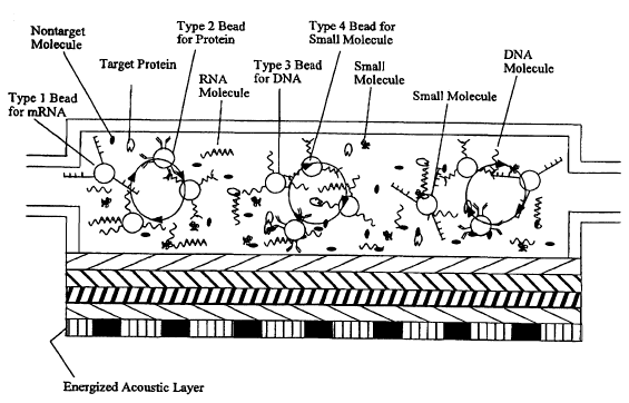
Figure 8 is a schematic representation of a cross-sectional view of the
chamber with
2S four different types of beads in a solution being introduced into the
chamber. The
'Four types of the beads, type 1, type 2, type 3, and type 4 are used for
capturing target
mRNAs, target proteins, tar~~ot DNAs, and target small molecules,
respectively.
)Figure 9A is a schematic r417resentation of a crass-sectional view of the
chamb er with
the target cells being lysed car disrupted to release their components.
CA 02424941 2003-04-04
WO 02/30562 PCT/USO1/42601
6
Figure 9~ is a schematic representation oCa cross-sectional view of the
chamber
showing the released camponents of the lysecl target cells.
Figure 10 is a schematic representation of a cross-sectional view of the.
chamber with
the acoustic elements being energized so that an acoustic mixing is provided
to
facilitate the binding of the molecules of interest to their respective beads
(energized
acoustic layer depicted by thick bold lines).
Figure 1~ is a schematic re~~resentation of a cross-sectional view of tile
chamber with
the molecules of interest being bound to their respective beads. Target
protein
molecules, DNA molecules. mRNA molecules and small molecules have been bound
type 2, type 3, type 1 and type 4 beads, respectively.
Figure 1BA is a schematic representation o1' a cross-sectional view of the
chamber
with the molecule-bead complexes being collected to the bottom surface of the
chamber under dielectrophoretic forces produced by energized DAP electrodes
(energized DEP electrode layer shown by thick bold lines).
Figure ~2>a is a schematic represen ration of a crass-sectional view of the
chamber
with the molecule-bead complexes being collected to the central region of the
bottom
surface of the chamber under traveling-wave dielectrophoretic forces produced
by
energized DEP electrodes.
Figure ~3A is a schematic representation oFthe top view ol~ the chamber with
the
electrodes on the particle switch layer being energized.
Figure 13B is a schematic representation o1' the top view of the chamber
looking
through to the particle switch layer, illustrating the faur types of molecule-
bead
complexes being switched rind separated to the ends o~ three branches within a
particle switch when the elec:irodes in the particle switch are energized with
phase-
shifted electric signals.
CA 02424941 2003-04-04
WO 02/30562 PCT/USO1/42601
Figure 13C is a schematic representation ol=the top view ol=the chamber
illustrating
the tour types of molecule-head complexes switched and separated to three ends
ol~
the chamber.
Figure 1~A is a schematic representation ol~ a three-dimensional perspective
view ol~ a
DNA-analysis chamber showing the DNA probe layer.
Figure ~~~ is a schematic representation ol~a three-dimensional perspective
view o~
a DNA-allalySIS Chamber ShoW111g the traVellllg-Wave dleleGtrOphOreSlS (TW-
DE~)
Electrode layer. The detailed electrical connections a~such TW-DEP elECtrodes
to a
signal source that can produce at least 3 phase-shifted signals having the san
1e
frequency are not shown.
Figure 1~C is a schematic rEpresentation of a three-dimensional perspective
view of~ a
DNA-analysis chamber showing the magnetic sensor layer. Th a letter "S"
represents
"sensor".
Figure 1~1~ is a schematic representation of~ a three-dimensional perspective
view of a
DNA-analysis chamber showing that the traveling-wave dielectrophoresis layer
being
energized, and the energized traveling-wave dielectrophoresis electrodes
moving the
DNA-bead complexes into the chamber (Energized electrode layer depicted with
thick
bold lines). The DNA-analypsis chamber comprises a chip having a DNA probe
layer
(top layer), a traveling-wave DEP layer, and a magnetio sensor layer
'?0 Figure .14E is a schematic representation ol~ a three-dimensional
perspective view of~ a
D ~ 'A-analysis chamber showing that the DNA-head complexes are dispersed into
the
chamber and target D ~ ~A molecules hybridized to the beads are also
hybridized to the
DNA probes on the chip.
Figure ~4F is a schematic representation of a three-dimensional perspective
view o1' a
?5 DNA-analysis chamber showing that the single-stranded portions of the
target DNA
molecules ell the DNA-bead complexes are hybridized to the DNA probes an the
chip
that are localized to magnetic sensors. The prGSCnce and the number ol'tIIG
magnetic
beads are detected with the magnetic sensors (energized magnetic sensor layer
CA 02424941 2003-04-04
WO 02/30562 PCT/USO1/42601
8
depicted with thick bold lines). 1~o illustrate that magnetic sensors are
responsive to
the presence of the magnetic beads, individual magnetic sensors are
schematically
shown, although these sensor elements cannot be seen from the top of the
chamber.
Figure SSA is a schematic representation oj~ a three-dimensional perspective
view of
the protein/mRNA-analysis chamber that comprises a chip showing the nucleic
acid
probel antibody probe layer (top layer) of the chip.
)figure ll~~ is a schematic representation ofi a three-dimensional perspective
views of
the protEI11lI11RNA-allalySIS ehambel' S110Wlllr' tllE tl'aVGllllg-WAVE
dlElectl'0(1110I'eSIS
electrode layer of the chip. 'I°he detailed electrical connections of
such TW-DEP
electrodes to a signal source that can produce at least 3 phase-shifted
signals having a
same frequency are not shown.
Figure ASC is a schematic representation ol~ a three-dimensional perspective
view ol=
the proteilllmRNA-analysis chamber showing that the protein-bead complexes and
mRNA-bead complexes art dispersed into the chamber using traveling-wave
dielectrophoresis (energized electrode layer depicted with thick bold lines).
Figure 15D is a schematic representation of a three-dimensional perspective
view of
the protein/mRNA-analysis chamber showing that the protein molecules and mRNA
molecules are decoupled or dissociated front the beads and have begun to bind
specific binding partners on the chip surface.
Figure 15>C is a schematic representation of a three-dimensional perspective
view of a
proteinlmRNA-analysis chamber showing that the protein molecules and mRNA
molecules are bound to the antibody-probes and nucleic acid probes
respectively,
Detestably-labeled binding partners are bEint~ introduced to the
proteilll111RN~A-
allalySlS chamber' I'I'olll a pt51'l. ~rllC beads ll~lrC heell re111QVeC1
11'olll the I:11a111bC'.1' or' the
?5 detection regions or' the chamber by travslin~~-wave dielectrophoresis
Forces by
energizing 'f W-DGl' electrodes (not shown) or by fluid flow forces durin~~
the process
of introduction of the detestably-labeled (fluol-s-scence-labeled) binding
molecules
(not shown).
CA 02424941 2003-04-04
WO 02/30562 PCT/USO1/42601
9
Figure 15F is a schematic representation oi~ a three-dimensional perspective
view o(~ a
proteinlmRNti-analysis chambei° showing that the fluorescence-labeled
binding
molecules are bound to the protein molecules and to the mIZNA molecules that
have
bound to the probes on the chip.
Figures ~6A and I$ are schematic representations of a three-dimensional
perspective
view of a small-molecule analysis chamber comprising a chip at the bottom. The
chip
has a fluidic channel layer (~), and a traveling-wave DEP layer (B). The
detailed
electrical connections of the traveling-wave UEP electrodes to a signal source
that can
generate at least 3 please-shi ited signals having tile same frequency are not
shown.
Figure 1.6C is a schematic representation of a three-dimensional perspective
view of
the small-molecule analysis chamber showing that the small-molecule-bead
campiexes are moved to the central regions of the channel using traveling-wave
dielectrophoresis (active electrode layer depicted with thielc bald lines).
Figure Jt6d) is a schematic representation of a three-dimensional perspective
view oi'
the small-molecule analysis chamber showing that the small molecules are de-
coupled
or dissociated from the beads. The beads have been moved out of the chamber by
traveling-wave dielectrophoresis (not spawn). The molecules are then labeled
with
florescence molecules (not shown).
Figure ~6;IJ is a schematic representation of a three-dimensional perspective
view of
small-molecule analysis chamber showing that the small molecules are directed
through the channel under electrophoresis ar Llectro-asmosis elects.
Figure 16F is a schematic representation of a three-dimensional perspective
view of
small-molecule analysis opamber showing that the small molecules are directed
through the channel and art' detected by an ol~(=chip iluoresoence detector_
2~ Figure 17 depicts a single chip integrated biochip system, in which the
Chip is part o(~
a chamber, and the cover ol~ the chamber has inlet ports for the application
ol~ a sample
and the addition of reagents. ante outlet ports for the outflow oi~ waste.
'1'hrc~e separate
CA 02424941 2003-04-04
WO 02/30562 PCT/USO1/42601
axeas of the chip are used for sample processin~~ (areas A and 13) and
analysis (C), and
each area ofthe chip has dil~lcrent functional or~r~s.
Figure 18 depiots a single chip integrated biochip system, in which the chip
is part of
a chamber, and the cover ol~ the chamber has inlet ports for the application
o1' a sample
acid the addition of reagents. and outlet ports I-or the outflow of waste.
'T'11e chip
comprises a particle switch that can direct sample components to different
areas of the
chip for further pracessing and analysis tasks.
Figure >19A is a top view of a multiple force chip capable of producing
dielectrophoretic foi°ces from an upper layer having interdigitated
Electrodes and
electromagnetic forces from a lower layer having electromagnetic elements.
Figure )19~ is a tap view through the chamber comprising the multiple lorcc
chip
showing a diluted blood sample introduced into the chamber.
Figure J19~ is a top view through the chamber comprising the multiple force
chip
showing white blood cell collected at the edgea of the interdigitated
microelectrode
array by positive dielectrophoretio forces.
)Figure ~.9D is a top view through the chamber comprising the multiple irrcc~
chip just
after the addition of a lysis buffer that contains magnetic beads with oli~~c>-
Cd°C)~~
modified surfaces.
Figure I9>E is a top view through the chamber comprising the multiple
foi°ce chip
showing the capture of the magnetic beads at the poles of activated magnetic
elements.
lNigu~~e ><9F is an image of tm agarose gel showing an RT-PCTZproduct
~aoneratiy
li~om mRNA recovered from the captured magnetic beads.
JO
CA 02424941 2003-04-04
WO 02/30562 PCT/USO1/42601
SUMMARY
The present invention recognizes that analytical techniques that can he uselul
in medical diagnosis, forensics, genetic testing, In°ognosties, and
pharmacoge«omies,
and research often require extensive preparation of complex biological
samples.
Preparation of biological samples such as blood samples can require multiple
steps
such as centrifugation, filtering, and pipeting, and steps that involve lysis
procedures,
incubations, enzymatic treatments, gel purification of nucleic acids or
proteins, etc.
Such steps are time-consuming, labor intensive, and diffcult to standardize.
The
present invention recognizes that an automated integrated system that can
perform
both sample preparation and sample analysis can standardize and streamline
testing
procedures from sample to result, representing, i~z effect, a "lab on a chip"
that
requires minimal manual intervention. In addition, such systems can be
designed to
analyze multiple sample components at once, reducing the need for multiple
samples
to be taken from a single source, greatly accelerating the process of
diagnasis,
assessment, or investigation.
The present invention also recognizes that the ability to manipulate
particles,
such as culls and microparticles bound to sample components using applied
physical
forces, can be utilized to automate, streamline; sample processing and
analysis. These
methods of manipulating sample components for sample processing (or sample
?0 preparation) and analysis can be utilized for a variety of purposes, such
as the
detection of particular molecules, compounds. or nucleic acid sequences in
samples,
for use in the diagnosis or prognosis of disease states, conditions, or
infection with
etiological agents, in the identification of subjects, in the genetic
screening of
subjects, and other applications.
'?5 A first aspect of the invention is an integrated biochip system that
comprises a
single chip, wherein the chip can perform at least two sequential taslcs, and
at least
one of the tasks functions in the pracessing ol~ a sample. frcferably, at
least one task is
performed by the application of physical forces that are in part generated by
micro-
scale structures that are built info or onto a chila. freferabIy, at least one
to s1: is
30 performed by the manipulation of binding partners that are coupled to a
sample
moiety. An integrated biochip system is preferably automated.
CA 02424941 2003-04-04
WO 02/30562 PCT/USO1/42601
l
A second aspect of the invention is an integrafed biochip system that
comprises two ar more chips and can perform at (east two sequential tas(a
using two
or more chips of the integrated system, wherein at least one of the chips
aC'the system
can pei°form at least one task in the preparation of a sample.
Preferably, un integrated
S biochip system comprising two or more chips is automated, and at least two
of the
chips of the system can be in fluid communication with one another.
Translocation of
sample components from at least one chip oi= the integrated biochip system to
at least
one other chip of the integrated biochip system is preferably by a mechanism
other
than fluid flow, mast preferably through tho application of physical forces.
Preferably, at least one task is performed by the application of physical
farces
that are in part generated by micro-scale structures that are built into ac
onto a chip, al
least one task can be performed by the manipulation of binding partners that
are
coupled to a sample moiety.
A third aspect ofthc invention is a method ofusin g a system of integrated
1.S chips for processing and analyzing samples. ~hhe method includes the
application of a
samplo to the system and performing at least two sequential tasks in the
processing
and, optionally, analysis, of a sample. At least one processing task can be
performed
by the integrated system using applied physical forces that are in part
generated by
microscale structures an the surface of a chip aF the system. Preferably but
optionally
the processing stop can include the manipulation of sample moieties coupled to
micraparticles.
DETAILED DESCRIPTION Oi° 'I"IiE INVENTION
DEFINITIONS
2S Unless donned otherwise, all technical and scientific terms used herein
have
the same meaning as commonly understood by one of ordinary skill in the art to
which this invention belongs. Generally, the nomenclature used herein and the
manufacture or laboratory procedures described below are well known and
commonly
employod in the art. C:anventional mothods art used far these procedures. such
as
those provided in the art and various general re ferences. 'I'crms of
orientation such as
"up" and "down" or "upper's or °'lower" and the like refer to
orientation of~ parts
during use of a device. Where a term is provided in the singular, the
inventors also
CA 02424941 2003-04-04
WO 02/30562 - PCT/USO1/42601
li
contemplate the plural of tlntt term. The nomenclature used herein is well
known and
commonly employed in the nrt. Where there are discrepancies in terms and
definitions used in references that are incorporated by reference, the tern ~s
used in this
application shall have the dclunitions given herein. As employed throughout
the
disclosure, the following terms, unless otherwise indicated, shall be
understood to
have the following meanings:
An "integrated chip system'', "integrated biochip system", a "system of
integrated chips", a "system of integrated biochips" ar "system" is at least
one chip
that can perform at least two sequential tasks in the processing and analysis
of a
sample, in which at least one task performed by the integrated biochip system
is a
processing task.
A "task'" is a function in the processing or analysis of a sample. A task can
comprise more than one stela. For example, a separation task can comprise
mixing and
binding steps that facilitate the separation.
A "fun coon" performed by a chip o(= a system of the present invention can be
a
task, such as a processing ar analysis task, or can be another function that
occurs
between tasks or as part of a task and facilitates the performance of the
task. One
example of a non-task function is a mixing function, such as a mixing function
that is
performed by acoustic forces on a chip that facilitates dispersion andlor
binding of
sample components. Another example of a non-task function is a translocation
of
moieties from one chip to another chip, or from one area of a chip to another
area of a
chip, such as by electrophoresis. dielectrophoresis, traveling wave
dielectrophoresis,
or traveling wave magnetophoresis.
A "processing fiask'~ is a procedure in the processing of a sample. (
Processing
'?5 of a sample is also referred to as sample preparation,) Generally a
processing task
serves to separate components of a sample, translocate compon ents of a
sample,
focus, capture, isolate, con ccntrate, or enrich components of a sample. at
least
partially purify components of a sample, or disrupt or structurally alter
ctunl~anents ol~
a sample (for example, by Ivrsis, denaturation. chemical modification, or
hintling of
components to reagents). A processing step can net on one type of sample
component
to release, expose, modify, c,r generate another type of sample component that
can be
used in a further processing or analysis task. li"c,r example, a cell can be
Ivpscd in a
CA 02424941 2003-04-04
WO 02/30562 PCT/USO1/42601
1 ~l
processing step to release nucleic acids that can be separated in a further
processing
task and detected in a subsccluent analysis task. Binding or coupling can he a
step in a
pi°ocessing task, where binding or coupling, particularly the coupling
ofa sample
component to a binding partner such as a microparticle, facilitates the
se:paralion,
translocation, capture, isolation, focusing, concentration, enrichment,
structural
alteration, or at least partial purification of at least one component of a
sample,
Mixing can also be a step in a processing task, where mixing facilitates the
binding,
separatian, translacation, concentration, structural alteration, or at least
partial
purification of at least one component of a sample.
An "analysis task" is a task that determines a result of a sample larocessin g
and
analysis procedure, and can be an assay, such as a binding assay, a
biochemical assay,
a cellular assay, a genetic assay, a detection assay, etc. Generally an
analytical task
determines the presence, amount, or activity of a sample component. Binding ar
coupling can be a step of an analysis task, where binding or coupling
facilitates the
detection or assay of at least one component of a sample. Mixing can also be a
step of
an analysis task, where mixing facilitates the binding, detection, or assay
ol=at least
one component of a sample.
"Sequential" means following a particular order, where followings a particular
order of tasks, for example. is necessary to ~~chieve the desired final
result. In an
2Q integrated biochip system ol~ fihe present invention, taslcs are performed
sequentially to
abtain a final result. When two tasks are performed sequentially, a second
task uses
one ar more products of the first task, where ''product" can mean a sample
component
that was separated, at least partially purified, or concentrated in the first
step, or a
sample component that was the result of a denaturing or lysing step, was
subjected to
a biochemical reaction ar away. became bound to a reagent, etc., in a previous
task.
As used herein. "first" and "second" do not rcFer to their absolute order in
the
integrated system, but rather to their relative order, where a process
performed on the
second chip occurs after a process performed on the first chip.
A 'xcllip'~ is a surFacr on which at least one manipulation or process. such
as a
iranslocation, separation, capture, isolation, lr~cusing, enrichment,
concentration.
physical disruptian. mixing. binding, or assav° cm be performed. A
chila can he a solid
or semi-solid substrate, porous or non-porous on which certain processca, such
as
CA 02424941 2003-04-04
WO 02/30562 PCT/USO1/42601
1i
physical, chemical, biological, biophysical or biochemical processes, eic..
can be
carried out. A chip that performs more than one lunation can have combinations
of
one or more different Functional elements such specific binding members,
substrates,
reagents, or different types of micro-scale structures that provide sources of
different
physical forces used in the processes carried out on the chip. Chips can be
multiple
force chips, in which differs nt functional elements can be pravided on the
same
surface, or in different structurally linked substrates or layers (where a
layer is a
surface that supports substrates, micra-scale structures, or moieties to be
manipulated)
that are vertically oriented with respect to cue another. For descriptions of
multiple
I 0 force chips, see United States Application IW unber 091679,024 having
attorney docket
number 4718~12000~100, Entitled "Apparatuses Containing Multiple Active I~orce
Generating Elements and Uses Thereof' filed October ~l, 2000, herein
incorporated by
reference in its entirety.
Micro-scale structures such as but not limited to channels and wells,
electrode
elements, electromagnetic elements, and piezoelectric transducers are
incorporated
into, fabricated on, or otherwise attached to the substrate for facilitating
physical,
biophysical, biological, biochemical, or chemical reactions or processes on
the chip.
Tlve chip may be thin in one dimension and may have various shapes in other
dimensions, for example, a rectangle, a circle, an ellipse, or other irregular
shapes.
The size of the major surface of chips of the present invention can vary
considerably,
e.~:, from about 1 mm'' to ahout 0.25 m~. Pre:ferably, the size of the chips
is from
about ~. mm2 to about 25 cm~ with a characteristic dimension from about I mm
to
about 5 cm. The chip surfaces may be flat, or not flat. The chips with
non=Ilat
surfaces may include channels or wells fabricated on the surfaces.
~5 '°Micro-scale structures" are structures integral to or attached on
a chip or
chamber that have characteristic dimensions of scale for use in microfluidic
applications ranging ti~om about 0.1 micron h~ about 20 nun. hxample o 1 micro-
scale
structures are wells, channels, scaffolds, electrodes, electromagnetic units,
piezoelectric transducers, metal wires or films. feltier elements, micro
lubricated
pumps or valves, microfabricated capillaries car tips, or optical elements. A
variety ol~
micro-scale structures are disclosed in United States Patent Application
Number
09I67t),024, having attorney docket number ~718~12000~10(l. en titled
c'Ahparatuses
CA 02424941 2003-04-04
WO 02/30562 PCT/USO1/42601
1O
Containing Multiple Active: force Generating ~;lements and uses Thereof-"
lined
October 4, 2000, herein incorporated by reference in its entirety. Micro-scale
structures that can, when energy, such as an electrical signal, is applied.
generate
physical forces useful in the present invention, can be referred to as
"physical Force-
s generating elements" "physical force elements'", ''active Force elements'-,
or "active
elements".
"Substrate'" refers to fine surface of a chip where a moiety to be manipulated
can be held and manipulated. A substrate can be hydrophobic or hydrophilic, or
a
combination thereof and can comprise materials such as silicon, rubber, glass,
one or
snore ceramics, plastics, polymers, or copolymers. The substrate can be soled
or semi-
solid, can comprises one or more channels or wells, and can support micro-
scale
structures and functional elements such as specific binding members,
substrates,
reagents, or catalysts.
An "electrode" is a structure of highly electrically conductive material. A
highly conductive material i5 a material with a conductivity greater than that
of
surrounding structures or materials. Suitable highly electrically conductive
materials
include metals, such as gold. chromium, platinum, aluminum, and the like. and
can
also include nonmetals, such as carbon and conductive polymers. An electrode
can be
any shape, such as rectangular, circular, eastellated, etc. Electrodes can
also comprise
doped semi-conductors, where a semi-conducting material is mixed with small
amounts of other conductive materials.
A "chamber" is a structure that that is capable of containing a t"luid sample
and
preferably comprises at least a portion of a chip.
A "port" is an opening in a chamber through which a Fluid sample can enter or
exit the chamber. A port can be of any dimensions, but preferably is of a
shape and
size that allows a sample to he translocated through the porn by physical
Forces, or
dispensed through the port 1y> means of a pipette. syringe, or conduit. or
other means
of applying a sample.
A "conduit"' is a means For fluid to be transported From a container to a
chamber of the present invention. Preferably a conduit enga~~es a porfi in a
chamber. A
conduit can comprise any material that permits the passage of a l7uid
tlzrc~ut~h it.
Preferably a conduit is tubin~~, such as, for t~~tunhle, rubber, "I"el7on
CA 02424941 2003-04-04
WO 02/30562 PCT/USO1/42601
17
{polytetral7uoroethylene), or tygon tubing. A conduit can be of any
dimensions. buff
preferably ranges From 10 microns to 5 millimeters in internal diameter.
A "well" is a structure in a chip, with a lower surface surrounded on at least
two sides by one or more walls fihafi extend I-rom fihe lower surface of the
well or
channel. The walls can extend upward from the lower surFace of a well ar
channel at
any angle or in any way. The walls can be o(~an irregular conformation, fihafi
is, they
may extend upward in a sigmoidal or otherwise curved or multi-angled C~ashiou.
The
lower surface of the well or channel can be at the same level as the upper
surface of a
chip or higher than the upper surface of a chip, or lower than fine upper
surface of a
chip, such that fihe well is a depression in the surf ace of a chip. 'The
sides or walls of a
well or channel can comprise materials ofiher fihan thaw that make up the
lower
surface of a chip. In this way the lower surface of a chip can comprise a thin
material
fihrough which electrical (including electromagnetic) forces can be
transmitted, and
fine walls of one or more wells andlor ono or more channels can optionally
comprise
I S other insulating materials that can prevent the: transmission of
electrical Forces. The
walls of a well or a channel of a chip can comprise any suitable material,
including
silicon, glass, rubber, and/or one or more polymers, plasfiics, ceramics, or
metals.
A "channel" is a structure in a chip wifih a lower surface and afi least two
walls
that extend upward from the lower surface oFthe chamlel, and in which the
length of
2Q two opposite walls is greater fillan fine distance between the two apposite
walls. A
channel therefore allows fan Ilow of a fluid along its internal length. A
i:hannel can be
covered ~a "tunnel") or open.
An "active chip" is a chip that comprises micro-scab structures that are built
into or onto a chip that when energized by an external power source can
generate at
Z5 least one physical Force that can perform a prooessing step or task or an
analysis step
or task, such as, but not limited to, mixing, iranslocation, Focusing,
separation,
concentration, capture, isolation, or enrichment, An active chip uses applied
physical
forces to promote, enhance, or facilitate desired biochemical reactions or
processing
steps or flasks or analysis steps or tasks. On an active chip, "applied
physical Forces '
30 are physical farces thafi, when energy is provided by a power source that
is external fio
an active chip, are generated by micra-scale structures built into or onto a
chip.
CA 02424941 2003-04-04
WO 02/30562 PCT/USO1/42601
18
A ''passive chip" is a chip that daes not utilize externally applied physical
forces to manipulate or control molecules and particles for chemical,
biochemical, or
biological reactions. Instead, the reaction process on a passive chip involves
thermal
diffusion of molecules and particles and involves naturally occurring farces
such as
the earth's gravity.
An "electromagentic chip" is a chip that includes at least one electromagnetic
unit, such as a micro-electromagnetic unit. The electromagnetic unit can be on
the
surface of a chip, or can be provided integrally ar at least partially
integrally, within
said chip. her example, an electromagnetic unit can be provided on the surface
of a
I 0 chip or can be imbedded within a chip. Optionally, an electramagnetic unit
can be
pal-tially imbedded within a chip. Preferred electromagnetic chips are those
disclosed
in United States Patent Application Serial Number 09/399,299 (attol°ney
docket
number ART-OOl O~.P.1), tiled September 17, 1999, entitled, "Individually
Addressable Micro-Electromagnetic Unit Array Chips" and United States Patent
15 Application Serial Number t)9/685,410 (attorney docket number ART-001
p4.P.1.1 ),
filed October 10, 2000, entitled, "Individually Addressable Micro-
Electromagnetic
Unit Array Chips in Horizontal Configurations', both herein incorporated by
reference in their entireties.
"Particle switch chip'" refers to the chip disclosed in United States
Application
20 Number 091678,263 (attorney docket number AI2TLNC0.002A), entitled
"Apparatus
for Switching and Manipulating Particles and Methods of Use Thereof' laled on
October 3, 2000, incorporated by reference in its entirety, comprising al
least three
sets of electrodes that are independent of one another, that can translocatc
particles
using traveling wave dielectrophoresis or traveling wave electrophoresis, and
that can
?5 be used to move particles alr~ng different pathways connected at a common
branch
point when the sets afelectrodes are connected to out-of=phase signals.
A "multiple force chip" or "multiforcc chip" is a chip that generrltes
physical
force fields and that has at least two different types of built-in structures
each of
which is, in combination with an external power source, capable oj~ generating
one
30 type of physical 1-7eld. A ful I description of th c multiple Force chip is
provided in
United States Application Number 091679,0'' having attorney docket number
~~18i~?000~00, elltltled "<~l~yal'atLISC~ COllttllillll~~ Mllltlple ActIVe
f"()1'eC.' (it'll('I'~1t111
CA 02424941 2003-04-04
WO 02/30562 PCT/USO1/42601
1~
Elements and Uses Thereol-' Filed Uctober ~. ~t)00, herein incorporated by
rclcrence
in its entirety.
"Mixing" as used herein means the use of physical forces to cause particle
movement in a sample, solution, or mixture (such as a mixture of sample and
sample
solution, or a mixtm°e or moieties and binding partners), or to cause
mavement of
sample, solution or mixture that is contained in a chamber such that
components of
the sample, solution, or mixture become interspersed. Preferred methods of
mixing for
use in the present invention include use of acoustic forces and thermal
convection.
''Disruption" as used herein means changing the struotural state of a sample
component. Examples of disruption are cell lysis, denaturation of proteins,
and
dissociation of subunits of complexes, such as, for example, ribosomes.
Disruptions
can be effected through the use of physical forces, such as for example, high
voltage
electric fields or acoustic forces, or by use of reagents such as denaturing
agents,
chelating agents, surfactants, or enzymes.
"Piezoelectie transducers" are structures capable ol=generatiug an acoustic
field in response to an electrical signal. Preferred piezoelectric transducers
arc
piezoelectric ceramic disks or piezoelectric thin films covered on both
surfaces with a
metal film.
"Electromagnetic units" are structures that, when connected to a source of
electric current, can produce a magnetic hold and exert a magnetic force on
magnetic
or paramagnetic particles. L;lectromagnetic units preferably include a core
that is
preferably magnetic or maf~netizable, and a means, such as a conducting coil,
for
conducting an electric current about said magnetic core.
"Fluid flow" refers tc~ the mass flow ol~ (laid by means such as by
electrophoresis or mechanic,.il force, such as laressure or thermal convection
forces.
"Autamated" means not requiring manual procedures, such as pipeting or
other manual transfer of samples or reagents. inversion or vortexing of tubes,
placing
samples in a centrifuge, incubator, etc. by a practitioner, anel the like. IAn
automated
system may, however, require manual application oi~th~ sample to the system
(i.e., by
3(~ laipeting or injecting), or manual recovery ol~sample components that have
been fully
processed by tl~e system (i.c.. by pipeting tiwm a chamber, or collecting iv a
tube that
a conduit leads into). An automated system many c7r may not require a
practitioner to
CA 02424941 2003-04-04
WO 02/30562 PCT/USO1/42601
Ca17t1'Ol pOWel'-dl'IVell Sy5tel77s f01' j~Llld flaw. to Galltl'O1 powel'-
dl'1Ve11 SyStel115 la l'
gellel'atlllg phySlGa1 farCeS 1a1' tile pel'tar111a17CG aI' pl'oCeSSlllg alld
allalySIS tEiSl<S, to
control power-driven systems For generating physical forces for the
translocation oI~
sample canlpon ents, and the like, during the operation of the integrated chip
system.
5 An automated system, such as an automated integrated biochip system of the
present
invention, is preferably but optionally programmable.
As used herein, "physical field," e.g., used itself ar used as "physical field
in a
region of space" ar "physical field is generated in a region o~ space" means
that the
region of space leas fallowin~~ characteristics. When a Illoiety of
appropriate
10 propel'ties is introduced into the region of space (i.e. into the physical
field), Forces are
produced on the moiety as a result of the interaction between the moiety and
the field.
A moiety Gan be manipulated within a field via the physical forces exerted on
the
moiety by tile field. Dxemplary fields include electric, magnetic, acoustic,
optical and
velocity fields. In the present invention, physical field always exists in r1
medium in a
15 region of space, and the moiety to be manipulated is suspended in, ar is
dissolved in,
ar mare generally, is placed in the medium. 1"ypically, the medium is a fluid
such as
aqueous or noel-aqueous liquids, or a gas. Depending an the field con
fiiguratian, an
electric field may produce electrophoretiG forces on charged moieties, or may
produce
conventional dielectcophoretic forces and/or traveling wave dielectrophoretic
forces
20 on charged and/or neutral moieties. Magnetic fuelds may produce magn etic
forces on
magnetic moieties (inclLldint~ paramagnetic moieties, or tra~~eling-wave
magnetophoretic farces on magnetic moieties. Acoustic field may produce acou
stic
radiation forces on moieties. Optical field may produce optical radiation
farces on
moieties. Velocity field in the medium in a region of space refers to a
velocity
distribution of the medium that moves in the reunion a~ the space. Various
mechanisms play be responsible far causing the medium to move and the medium
at
different positions may exhibit different velocities, thus generating a
vGloGiiy field. A
velocity field may exert mechanical Farces on moieties in the n7ediun7.
As used herein, "phi°aical force" ref~ra to any Force that moves l~hrv
moieties or
their binding partners withcmlt chemically or biologically reacting with t17~
moieties
and the binding partners, or with minimal chemical or biolo~~ical reactions
with the
binding partners and the moieties sa that the bialogicallchenlical
Functions/praperties
CA 02424941 2003-04-04
WO 02/30562 PCT/USO1/42601
21
of the binding partners and the moieties are not substantially altered as a
result of such
reactions. Throughout the typlication, the team of "Forces'" or ''physical
li~rcc~s"
always means the "Forces" ~~r "physical forces" e:xeuted on a moiety ar
moieties. 'I"he
"forces" or ''physical forces" are always generated through "fields" or
''physical
Gelds". The forces exerted on moieties by the 1-fields depend on the
properties of the
moieties. Thus, for a given lueld or physical field to exert physical forces
on a moiety,
it is necessary for the moietv° to lave certain properties. While
certain types of fields
may be able to exert farces on different types of moieties laving different
properties,
other typos of fields may be able to exert forces on only limited type of
moieties. Far
example, magnetic field can exert forces or magnetic forces only on magnetic
particles or moieties having certain magnetic laroperties, but not on other
particles,
e.g,, polystyrene beads. On the other hand, a non-uniform electric field can
exert
physical forces on many types of moieties such as polystyrene beads, cells,
and also
magnetic particles.
As used here in, "electric forces" (or ''electrical Forces") are the Forces
exerted
on moieties by an electric (or electrical) field.
"Electric field pattern" refers to the field distribution, which is function
oFthe
frequency of the field, the magnitude of the field, the geometry of the
electrode
structures, and the frequency and/or magnitude modulation of fine field.
"Dielectric properties" of a moiety are properties fihat determine, at least
in
part, the response of a moiety to a dielectric iaeld. The dielectric
properties of a
moiety include the effective electric conductivity of a moiety and the
efFective electric
permittivity of a moiety. T'or a particle of homogeneous composition, for
example, a
polystyrene bead, the effective conductivity and effective pcrmifitivity arc
independent
?5 of the frequency of the electric field. For moieties of nonhomogeneous
composition,
For a example, a cell, the ei-1-active conductivity and eFfective permittivity
are values
that take into account the el~lective conductivities and effective
permittivities of both
the surface (membrane) and internal portion c~f~ the cell, and can vary wish
fine
frequency of the electric i~iclcl. In addition, the dielectric Force
experience by a moiety
3b in an electric field is dependent on its size; therefore, the coverall sire
ol'moietyr is
herein considered to be a dielectric property oFa moiety. Properties of a
moiety that
contribute to its dielectric properties include the net charge on a moiety:
ihc
CA 02424941 2003-04-04
WO 02/30562 PCT/USO1/42601
composition of a moiety (including the distribution of chemical groups or
moieties on.
Wlthln, Or t171'OLIghOLlt a 11701Cty~; SILe Of a II7C)Iety; 5u1'faCe
CClIIt1gL11'at1017 ()1'L117101ety;
surface charge of a moiety; and the conformation of a moiety.
A "dielectrophoretic force" is the force that acts on a polarizable particle
in a
nonuniform AC electrical IUc:ld. As used herein "dielectrophoresis" is the
n7ovement
of moieties in response to dielectric forces.
"Dielectrophoresis''_ sometimes called ''conventional dielectropl7oresis, is
the
movement of polarized particles in nonuniform electrical fields. There are
generally
two types ofdielectrophoresis, positive dielectorphoresis and negative
dielectrophoresis. In pasitive dielectrophoresis, particles are moved by
dielectrophoresis toward the strong field regians. In negative
dielectrophoresis,
particles are moved by dielectrophoresis toward weak field regions. Whether
moieties
exhibit positive or negative clielectrophoresis depends on whether particles
are more
or less polarizable than the surrounding medium.
"Traveling-wave dielectrophoretic (DGP) ford" refers to the force that is
generated on particles or molecules due to a traveling-wave electric field. An
ideal
traveling-wave field is characterized by the distribution of the phase values
ofAC
electric field components, being a linear function of the position of the
particle. A
traveling wave electric field can be established by applying appropriate AC
signals to
the microelectrodes appropriately arranged oll a ch 1p. For generating a
iraveling-
wave-electric field, it is necessary to apply at least three types of
electrical signals
each having a different phase value. An example to produce a traveling wave
electric
field is to use four phase-quardrature signals (0. 90, 180 and 270 degrees) to
energize
Four linear, parallel electrodes patterned on the chip surfaces. Such four
electrodes
may be used to form a basic. repeating unit. Depending on the applications,
there
may be more than two such units that are located next to each other. This will
produce a travelin l; electric field in the spaces above or near the
elecirodca. As long
as electrode elements are arr~lngod Following certain spatially sequential
orders,
applying phase-seduenced signals will result ill r°atablisl7ing
traveling electrical (welds
:30 in the region close to the electrodes.
As used herein, '°traveling wave dielecirophoresis"' is the
movement of
moieties in response to a traveling wave electric field.
CA 02424941 2003-04-04
WO 02/30562 PCT/USO1/42601
As used herein, "magnetic Forces" are the F01'GeS exerted on moieties by a
magnetic field.
"Traveling wave electromagnetic Force" refers to the Force that is generated
on
particles or molecules due to a traveling magnLtiG field or a traveling
nla~~n~tio wave.
"Traveling wave magnetophoresis" rulers to the movement of a magnetic
particle or magnetizable particle under the influence of a traveling magnetic
held or a
traveling magnetic wave generated by an array of electromagnetic units. The
individual electromagnetic units are arranged according to specific spatial
relationships among the units. >~or example. individual electromagnetic units
may be
of rectangular geometry and of equivalent lengths, alld microfabricated on
chips so
that the units are aligned and parallel to Each other, as depicted, for
example, in Figure
2~B oFUnited States Patent Application Serial I~lumber 09IG85,~10 and having
attorney docl~et number AR'f-00104.P.1.1, bled October 10, 2000, entitled,
"Individually Addressable Micro-Electromagnetic Unit Array Chips in I-Iorizon
cal
Configurations", which is incorporated by reference ill its entirety.
Traveling wave
magnetophoresis can be synchronized or continuous. In synchranized
maglletOphOre5lS, a I'C CLII'1'CSlt IS LlSed t0 I11ag11et1Ze lndlVIClLIal
eleGtl'Olllag11Gt1C L1111tS
within an array such that the electramagnetic units can be addressed
sequentially. The
sequentially addressed electromagnetic units arc energized in an order, sue(
as a
~0 predetermined order, such that a magnetic particle or magnetizable particle
trans~el's
ti°om one location to another, In continuous magnetophoresis, an AC
Gurrcnt is used
such that the electromagnetic units are addressed using currents that are out
o-F phase,
such as, but not limited to, about 90 degrees out of phase. Alternative phase
shifts can
also be utilized. The phase :shifts cause a travelin g magnetic wave or
traveling
magnetic 'field to form.
As a sed herein, "acoustic forces (or acoustic radiation Forces)" are the
forces
eYel°ted on moieties by an acoustic Feld.
As used herein, "optical (or optical raLliation) farces" are the Forces
exerted on
moieties by an optical field.
~0 A "sample'° is any fluid (roll which components are to be separated
or
analyzed. A sample can be From any source. such as an organism, '~rouh
ol~cr~~unisnls
1i'om the same or differont spGGics, from th-r c:nvirollmed, such as l~ronl a
htoiy oI~
CA 02424941 2003-04-04
WO 02/30562 PCT/USO1/42601
water or from the soil, or from a Food source or an industrial source. A
sample can be
an unprocessed or a processed sample. A sawplc can be a gas, a liquid, or a
semi-
solid, and can be a solution or a suspension, A sample can be an extract, for
example a
liquid extract of a sail or food sample, an extract of a throat or genital
swab, or an
extract of a fecal sample.
A "blood sample" as used herein can refer to a processed or unprocessed
blood sample, i.e., it can be a centrifuged, filtered, extracted, or otherwise
treated
blood sample, including a blood sample to which one or more reagents such as,
but
not limited to, anticoagulanCs or stabilizers have been added. A blood sample
can be
of any volume, and can be from any subject such as an animal or human. A
preferred
subject is a human.
"Subject" refers to any organism, such as an animal or a human. An animal
can include any animal, such as a feral animal, a companion animal such as a
dog or
cat, an agricultural animal such as a pig or a cow, or a pleasure animal such
as a
horse.
A "white blood cell" is a leukocyte, or a cell of the hematopoietic lineage
that
is not a reticulocyte or platelet and that can be found in the blood of an
animal.
Leukocytes can include lymphocytes, such as I3 lymphocytes or T lymphocytes.
Leukocytes can also include phagocytic cells, such as monocytes, macrophages,
and
granulocytes, including basophils, eosinophils and neutrophils. Leukocytes can
also
comprise mast cells.
A "red blood cell" is an erythrocyte.
"Neoplastic cells" refers to abnormal cells that grow by cellular
proliferation
more rapidly than normal and can continue to grow after the stimuli that
induced the
new growth has been withdrawn. hleoplastic cells tend to show partial or
complete
lack of structural organization and functional coordination with the normal
tissue, and
may be benign or malignant_
A "malignant cell" is a cell having the laroperty of locally invasive and
destructive growth and metastasis.
A ''stem cell" is an undifferentiated cell that can give rise, through one or
more cell division cycles, to at least one dil~lcr~ntiated cell type.
CA 02424941 2003-04-04
WO 02/30562 PCT/USO1/42601
A "progenitor cell" is a committed but undifferentiated cell that can give
rise,
through one or more cell division cycles, to at least one differentiated cell
type.
Typically, a stem cell gives rise to a progenitor cell through one or more
cell divisions
in response to a particular stimulus or set oI~ stimuli, and a progenitor
gives rise to one
5 or more differentiated cell types in response to a particular stimulus or
set o(~ stimuli.
An 'ketiological agent" refers to any etiological agent, such as a bacteria,
virus,
parasite or prior that can infect a subject. An etiological agent can cause
symptoms
or a disease state in the subject it infects. A human etiological agent is an
etiological
agent that can infect a human subject. Such human etiological agents may be
specific
10 for humans, such as a specific human etiological agent, or may infect a
variety of
species, such as a promiscuous human etiological agent.
A "component" of a sample or "sample component" is any constituent of a
sample, and can be an ion, molecule, compound, molecular complex, organelle,
virus,
cell, aggregate, or particle ol=any type, including colloids, aggregates,
particulates,
1 ~ crystals, minerals, etc. A component of a sample can be a constituent
entity of a
sample that has been exposed or: altered by processes performed before
application of
the sample to a system of the present invention, or by the methods of the
present
invention, such as methods performed by a system of the present invention. A
component of a sample can l)e soluble or insoluble in the sample media or a
provided
20 sample buffer or sample solution. A component ofa sample oar be in gaseous.
liduid,
or solid form. A component of a sample may he a moiety or may not be a moiety.
A ''moiety" or "moir''ty of interest" is rely entity whose manipulation in a
system of the present invention is desirable. A moiety can be a solid,
including a
suspended solid, or can be in soluble form. A moiety can be a molecule.
lVlolecules
25 that can be manipulated include, but are not limited to, inorganic
molecules, including
ions and inorganic compounds, or can be orf~anic molecules. including amino
acids,
peptides, proteins, glycoproic:in s, lipoproteins, glycolipoproteins, lipids,
lots, sterols,
sugars, carbohydrates, nucleic acid molecules. small organic molecules, or
complex
organic molecules. .~ moiety can also be a nlolccular complex, can be all
organelle,
can be one or more cells, including prokaryotic and eulcaryotic cells, or can
be one or
more etiological agents. including viruses, parasites, or priors, or portions
tll~reof~. A
11101ety Call alSO bC a CL'yStal. 111111e1'al, COl1o1C1_ ll'ag111el1t,
lIlyCC111C, dl'oplCi, 17u1)ble. t)I'
CA 02424941 2003-04-04
WO 02/30562 PCT/USO1/42601
76
the like, and can comprise one or more inor~~nllic materials such as
polynleric
materials, metals, minerals, Mass, ceramics, and the like. Moieties can alsc7
be
aggregates of molecules, complexes, cells, organelles, viruses, etiological
agents,
crystals, colloids, or fragments. Cells can be any cells, including
prokaryotic and
eul<aryotic cells. Eukaryotic cells can be of any type. Of particular interest
are cells
such as, but not limited to, white blood cells, malignanf cells, stem cells,
progenitor
Dells, fetal cells, and cells inFected with an etiological agent, and
bacterial cells.
Moieties Gan also be artificial particles such polystyrene microbeads,
microbeads of
other polymel° compositions. magnetic micorbeads, carbon nlicrobeads~
As used herein, "intracellular moiety" refers to any moiety that resides or is
otherwise located within a cell, i.~,, located in the cytoplasm or matriX
o~l=cellular
organelle, attached to any intracellular membrane, resides or is otherwise
located
within periplasm, if there is one, or resides or is otherwise located on cell
surface, i.e"
attached on the outer surface: of cytoplasm membl°ane or Gell wall, if
there is one.
As used herein, "nlalnipulation" refers to moving or processing at- the
moieties, which results ill one-, two- or three-dimensional movement of the
moiety, in
a Ghip format, whether within a single Ghip ar between or among multiple
chips.
Moieties that are manipulated by the methods of the present invention can
optionally
be coupled to binding partners, such as microparticles. Non-limiting eXamples
of the
manipulations include transportation, capture, Focusing, enrichment,
concentration,
aggregation, trapping, repulsion, levitation, separation, isolation or linear
or other
directed motion oCthe moieties. par effective manipulation of moieties coupled
to
binding partners, fine bindings partner and the physical force used in the
method must
be colnpatlble. ~'pl" eXanlpl(:. bllldlllg pal'tllel'S wlth InagIletIG
propertleS IllLlSt be LISed
with magnetic force. Similarly, binding partners with certain dielectric
properties,
c:.g,, plastic particles, polystyrene microbeads. Must be used with
dielectrophorelic
force.
As used herein, "th moiety to be manipulated is substantially coupled onto
surface of the binding partner" means that a majority of the moiety to be
mvnipLllat~d
3p is coupled onto surface of the binding partner anti can be manipulated by a
suitable
physical force via manipulation of the bindill~.~ partner. Ordinarily, at
least 1 t% of the
moiety to be manipulated is coupled onto surf-ace of the binding partner,
I'rGlerably,
CA 02424941 2003-04-04
WO 02/30562 PCT/USO1/42601
27
at least 5°l0, 10%, 20°r'°, 30°; r~.
~10°~'°, 50%. 60'~~, 70%, 80°l° or
90°f° of the moiety to be
manipulated is coupled onto surFacc oFthe binding partner.
As used herein, "the moiety to be manipulated is completely coupled onto
surFace of the binding partner" means that at least 90°l0 of the moiety
to be
S manipulated is coupled onto surface of the binding partner. Preferably, at
least 91 °Jo,
92%, 93°,~0, 9~t°J°, 95%, 96°f,.
97°r'°, 98°,~°, 99°/~ or
100°~° oFthe moiety to he
manipulated is coupled onto surface of the binding partner. A "solution that
selectively modifies red blood cells" is a solution that alters non-nucleat~:d
red blood
cells such that they do not interfere with the diclectrophorctic separation
o~l~ other cells
or components of a bland sample, without substantially altering the integrity
of white
blood cells, or interfering with the ability oFwhite blood cells to be
dielectrically
separated from other components of a blood sample.
"Binding partner" reFers to any substances that both bind to the moieties with
desired affinity or specificiiv and ace manipulatable with the desired
physical force(s).
l5 ~ ~on-limiting examples of the binding partners include cells. cellular
organelles.
viruses, microparticles or an aggregate or complex thereof , or an aggregate
or
complex of molecules.
A "microparticle" or "particle" is a structure of any shape and of any
composition, that is manipulatable by desired physical force(s). The
mieroparticles
used in the methods could hove a dimension from about 0.01 micron to about ten
centimeters. Preferably, the microparticles used in the methods have a
dimension
from about 0.1 micron to about several thousand microns, Such particles or
microparticles can be comprised of any suitable material, such as glass or
ceramics,
and/or one or mare polymers. such as, For example, nylon,
polytetrafi7uoroethylene
2~ (TEFLON ~~~~, polystyrene, holyacrylamide, scpaharose, agarose, cellulose,
cellulose
derivatives, or dextran, and~"or can comprise metals. Examples of
microparticles
include, but are not limited to, plastic particles. ceramic particles, carbon
particles,
polystyrene microbeads. glass beads, magnetic beads, hollow glass spheres,
metal
particles, pauticles of complex compositions. n~icroFabricated or
micromachined
particles, etc.
CA 02424941 2003-04-04
WO 02/30562 PCT/USO1/42601
"coupled" means bound. I~or example, a moiety can be coupled tc~ a
micraparticle by speciFic or nonspecific binding. As disclosed herein, the
binding call
be covalent or noncovalent. reversible or irrcvcrsible.
A "specific binding member" is one of two different molecules having an area
on the surface or in a cavity which specifically binds to and is thereby
defined as
complementary with a particular spatial and polar arganization of the other
molecule.
A specific binding member can be a member of an immunological pair such as
antigen-antibody, can be biotin-avidin or biotin streptavidin, ligand-
receptor. nucleic
acid duplexes, IgG-protein A, DNA-DNA, DNA-IZNA, RNA-RNA, and the like.
A "nucleic acid molecule°' is a polynucleotide. A nucleic acid molecule
can be
DNA, RIA, or a cambinatitm of both. A nucleic acid molecule can also include
sugars other than ribose and deoxyribose incorporated into fine backbone, and
thus can
be other than DNA or RNA. A nucleic acid can oomprise nucleobases that are
Naturally occurring or that do not occur in nature, such as xanthine,
derivatives of
Nucleobases, such as 2-aminoadenine, and the life. A nucleic acid molecule
ofth a
pl'eSent lllvelltlOn Gall have I I111CageS OtheI' than phOSphOdleSter
IInICageS. A llLlclele
acid molecule of the present invention can be a peptide nucleic acid molecule,
in
which nucleobases are linked to a peptide backbone. A nucleic arid molecule
call be
of any length, and can be single-stranded, double-stranded, or triple-
stranded, or any
combination thereof.
"I-Iomogeneous manipulation" refel's to the manipulation of pal'ticles in a
mixture using physical farces, wherein all particles of the mixture have the
same
response to the applied forcL~.
"Selective manipulation" refers to the manipulation of parficles using
physical
?5 l:orces, ill which differen t particles in a mixture have diflerl:llt
responses to the applied
Force.
"Separation'" is a process in which oNe or more components of a sample is
spatially sEparated from one or more other components of a sample. A se
l~aration can
be performEd such that one or more moieties oFinterest is iranslocatcd to one
or more
areas of a separation apparatus and at least se~nlc of the remaining
comlaonents are
translocated away from the clrea or areas where the one or more moieties of
interest
al'e traIlSlOCated t0 alld/~OI' rCtallled 111, Or I11 W111Ch One OI' 11101'e
111OIetleS 1;; I'Etalll(:d 111
CA 02424941 2003-04-04
WO 02/30562 PCT/USO1/42601
c~
one or more areas and at least some or the remaining components are removed
ti'om
the area or areas. Alternativ~c;ly, one or more components c>l~a sample can be
translocated to andlor retained in one or more areas and one or more moieties
can be
removed from the area or areas, and optionally collected. It is also possible
to cause
one or more moieties to be translocated to one or more areas and one ar more
moieties
of interest or one or more components of a sample to be translocated to one or
more
other areas. Separations can be achieved through the use of physical,
chemical,
electrical, or magnetic forces. Examples of (or ces that can be used in
separations are
gravity, mass flow, dielectrophoretic forces, and electromagnetic forces.
"Capture" is a type of separation in wi~ich one or mare moieties is retained
ill
one or more areas of a chip. A capture can be performed using a specif c
binding
member that binds a moiety of interest with high affinity.
An "assay" is a test performed on a sample or a component of a sample. An
assay can test for the presence of a conlponeni'. the amount or concentration
of a
component, the composition of a component. the activity of a component. etc.
Assays
that can be performed in conjunction with the compositions and methods o(= the
present invention include biochemical assays, binding assays, cellular-
assays, and
genetic assays.
A "reaction" is a chemical or biochemical process that changes the chemical
ar biochemical composition of one or more molecules or compounds or that
changers
the interaction of one or snore molecules with one or more other molecules or
compounds. Reactions of thG present invention can be catalyzed by enz~~nlcs,
and can
include degradation reactions, synthetic reactions, modifying reactions. or
binding
reactions.
A "binding assay" is an assay that tests l~or the presence or concentration of
an
entity by detecting binding ol~ the entity to a sheciFic binding member, or
that tests the
ability of all entity to bind another entity, or tests the binding affinity
ol~ one entity for
another entity. An entity can be an organic or inorganic molecule, a
nlolccular
t;omplex that comprises, or'~cmic, inorganic. t>r a combination of~ organic
ante inorganic
GO111pOLlIIdS, all OI'gallelle, a VII'L15, 01' a Cell. 13111c11ng aSSayS Call
LISe detectable IabelS
or signal generating systems that give rise to detectable signals in the
presence ol~ the
bound entity. Standard binding assays incluclc those that rely on nucleic acid
CA 02424941 2003-04-04
WO 02/30562 PCT/USO1/42601
~0
hybi°idization to detect speci tic nucleic acid sequences, those that
rely on antibody
binding to entities, and thaw that rely an ligands binding tt~ receptors.
A "biochemical assay" is an assay that tests for the presence, concentration,
or
activity of one or more components of a sample.
A "cellular assay' is fm assay that tests For a cellular process, such as. but
not
limited ta, a metabolic activity, a catabolic activity, an ion channel
activity, an
intracellular signaling activity, a i°eceptor-linlceci signaling
activity, a transcriptional
activity, a translational activity, or a secretary activity.
A "genetic assay" is an assay that tests For the presence or sequence of a
genetic element, where a genetic element can be any segment of a DNA or R~ ~A
molecule, including, but not limited to, a gene, a repetitive clement, a
transposable
element, a regulatory element, a telomere, a centromere, or DNA or RNA of
unknown
function. As nanlimiting examples, genetic assays can use nucleic acid
hybridization
techniques, can comprise nucleic acid sequencing reactions, or can use one or
more
polymerases, as, For example a genetic assay based on PCR. A genetic assay can
use
one or more detectable labels, such as, but not limited to, I7uorochromes.
radioisotopes, or signal generating systems.
A °'detection assay ~ is an assay that can detect a substance, sLicl~
as an ion,
molecule, or compound by producin g a detectable signal in the presence oFthe
substance. Detection assays can use specific binding members, such as
antibodies or
nucleic acid molecules, and detectable labels that can directly or indirectly
bind the
specif c binding member or the substance or a reaction product of the
substance.
Detection assays can also use signal producing systems, including enzymes or
catalysts that directly or indirectly praduce a detectable signal in the
presence oFthe
?5 substance or a product oFthc substance.
A "detectable label's is a compound ar molecule that eau be detected, or that
can generate a readout, such as fluorescence, radioactivity, color,
chemiluminescence
or other readouts known in the art or later developed. The readouts can be
based on
i7uorescence, such as by Iluorescent labels, such as but not limited to. C~v-
s, Cy-5,
p phycoerythrin, phycocyanin. allophycocyanin. 1' ITC, rhodamine. ar
lanthanides: and
by tloureseent proteins such as, but nat limited to. green Iluorescent protein
(Gl~ P).
'Fhe readout can be based on cnzvmatic activity such as, but not limited to,
the
CA 02424941 2003-04-04
WO 02/30562 PCT/USO1/42601
Jl
activity of beta-galactosidase, beta-lactamaso. horseradish peroxidase,
alkaline
phosphatase, or luciFerase. The readout can be based on radioisotapes Csuch as
~~P,
~I-1 , ~'~G, ~'S, ~Z~I, ~''P or ~~~1 ). A label optionally can be a base with
modified mass,
such as, Ior example, pyrimidines modified at the ~5 position or purines
modified at
the N7 position. Mass modiFyin g groups can be, (or examples, halogen, ether
or
polyether, alkyl, ester or polyester, or of the general type XR, wherein X is
a linking
group and R is a mass-moth lying group. One of skill in the art will recognize
that
there axe numerous possibilities for mass-modifications useful in modifying
nucleic
acid molecules and oligonucleotides, including those described in Oligonu
cleotides
and Analogues: A Practical Approach, Eclcstein, ed. (1991 ) and in
PGTiUS9~1100193.
A 'signal producing system" may have one or more components. at least one
component usually being a Labeled binding member. The signal producing system
includes all of the reagents required to produce or enhance a measurable
signal
including signal producing means capable oI~ interacting with a label to
produce a
signal. The signal producing system provides a signal detectable by external
means,
often by measurement of a change in the wavelength of light absorption or
emission.
A signal producing system pan include a cllromopharic substrate and enzyme,
where
chromophoric substrates arc enzymatically converted to dyes which absorb light
in
the ultraviolet or visible region, phosphors or lluorescers. However, a signal
producing system can also provide a detectable signal that can be based on
radioactivity or other detectable signals.
The signal producinf~ system can include at least one catalyst, usually at
least
one enzyme, and can include: at least one substrate, and may include two or
mare
catalysts and a plurality of u.ibstrates, and may include a combination of
onrvmos,
~5 where the substrate olvone enzyme is the praduct of the other enzyme.
'I'IZe operation
of the signal producing system is to produce a product which provides a
detectable
signal at the predetermined site, related to the presence of label at the
predetermined
site.
In order to have a dc:toctahle signal, it way be desirable to provide moans
For
amplifying the signal produced by the presence oFthe label at the
predetermined site.
Therefore. it will usually ho preFerable For the label to be a catalyst ar
luminescent
compound or radioisotope. most prcFerablv a catalyst. PreFerably. catalysts
arc
CA 02424941 2003-04-04
WO 02/30562 - PCT/USO1/42601
3~
enzymes and coenzymes which can produce a multiplicity of~ signal generating
molecules from a single label. An enzyme or coenzyme can be emhloycd which
provides the desired amplification by producing a product, which absarbs
light, for
example, a dye, or emits light upon irradiation, for Example, a fluoresces.
S Alternatively, the catalytic reaction can lead to direct light emission,
l:or example.
chemiluminescence. A large number of enzymes and coenzymes for providing such
products are indicated in U'.S. Pat. No. ~,275.1~9 and U.S. Pat. No.
x,318,9$0, which
disclosures are incorporated herein by reference. A wide variety of non-
enzymatic
catalysts which may be employed are found in LT.S. Pat. No. 4,160,d~15, issued
July
10, 1979, the appropriate portions of which are incorporated herein by
reference.
The product of the enzyme reaction will usually be a dye or t7uorescer. A
large
number of illustrative Eluorriscers are indicated in U.S. Pat. No,
~t,275,1~1C). which
disclosure is incorporated h crein by reference.
Other technical terms used herein have their ordinary meaning in the art that
they are used, as exemplified by a variety of technical dictionaries.
A SYSTt;ld9 OF I~'TE(:Itr~TGD CHIPS FOR TI-IE i'ROCESSING AND ANAL~I'SIS OF A
SAIViPI~E
The present invention includes an integrated biochip system for the processing
and analysis of a sample. Bv '°integrated biochip system" is meant a
system that: 1 J
comprises at least one chip. ?) is capable of laerForming at least two
seduential tasks
on a sample, wherein at least one task is a processing task. Preferably, at
least one
task performed by a system of integrated chips of the present invention
rccluires the
application at physical force by a source that 1s in part external to a chip
and in part
intrinsic to a chip, and prel~rably but optionallv, at least one sample
com~~onent is
manipulated through the use ofspecitie bindinr~ partners. such as
microhrtrticles. in a
task performed on at least one chip of a system ol' the present invention.
The present invention includes at least one chip, where a chip has a surface
on
which at least one separation, trap slocation. capturing procedure, assay, or
acoustic
mixing ox physical disrupticw process can bc~ le;rt'ormed. A chip can comprlsc
silicon,
glass, rubber, photoresist. or one or more mcials. ceramics. polymers.
cop>Ivmers. or
CA 02424941 2003-04-04
WO 02/30562 . . . PCT/USO1/42601
~3
plastics. A chip can comprise one or more flexible materials. A chip can he
from
about 1 mnh to about 0,25 :o~. Preferably, the sne of the chips useable in the
present
methods is ti-om about 4 mm~ to about 25 cm~. 'l'he steal?e ol~ the chips
useable in the
present methods can be regular shapes such as square, rectangular, circular,
or oval, or
can be irregularly shaped. The active surface ol~ a chip need not be flat, but
can be
curved, angled, etc. Chips useable in the methods of the present invention can
have
one or mare wells or one or more channels that can be etched or bored into a
chip or
built into or onto the surface: of a chip.
A chip can be part or' a chamber, can cn4~age a chamber, or can be at least
partially enclosed by a chamber, but this is not a requirement of the present
invention.
A chamber of the present invention is a structure that call contain a fluid
sample. A
chamber can be oh any size or dimensions, and preferably can contain a Iluid
sample
of between 0.001 mioroliter and 50 milliliters, more preferably between about
0.1
microliters and about 25 milliliters, and most preferably between about I
microliter
and about two milliliters. Preferably, a chamber comprises at least a portion
of at least
one chip. A chamber can comprise more than anc chip, or several chambers may
comprise, contact, or engage the same chip. A chamber can comprise any
suitable
material, for example, silicon, glass, metal, ceramics, polymers, plastics,
etc. and can
be of a rigid or flexible material. Preferred materials for a chamber include
materials
that do not interfere with the manipulation aF moieties in a sample, for
example,
insulating materials that do not bind charged or polarized molecules, such as
certain
plastics and polymers, for example, acrylic, or glass.
A chamber that coral?rises at least a portion of a chip useable in the methods
of
the present invention can comprise one or more ports, or openings in tile:
walls of a
2~ chamber. A port can be of any appropriate shape or size for the transport
or
dispensing of a sample, sample components, bur°fers, solutions, or
reagents through
the port. A port can be permanently open, or can comprise a flap or valve:
that allows
the part to be reversibly closed. A part can al?banally be an opening in a
wall that is a
common wall between two chambers. Alternatively, a port call provide an
opening in
a wall of a chamber- for the dispensing of sample into the chamber by, far
extlmple,
dlSpells111g 01' 111jeCtloll.
CA 02424941 2003-04-04
WO 02/30562 PCT/USO1/42601
3 ~1
A part can engage a conduit. A conduit can be any tube that allows for the
entry of a fluid sample, solution, or reagent into the chamber, or allows for
the
translocation of sample component or microparticles from one chamber to
another
chamber. Preferred conduits for use in the present invention include tubing,
for
example, rubber or polymeric tubing, e.g., tygon or Teflon~~~M
(polytetrafluoroethylene) tubing. Conduits that engage one or snore ports of a
chamber
can be used to introduce a sample, solution, reagent, or preparation by any
means,
including a pump for example, a peristaltic pump or infusion pump), pressure
source
syringe, or gravity feed.
Preferred chips in a system of the present invention include active chips.
Preferably, at least one chip in an integrated bioehip system of the present
invention is
an active chip. Active chips are chips that comprise micro-scale structures
that can
generate a physical force when energy is supplied to them From, for example, a
pawer
supply. Thus, the applied physical forces used in the methods of the present
invention
require an energy source (sometimes called a "signal source") and a structure
capable
of converting the energy to a type of force useFul in the present invention.
Active
chips are therefore described as chips that supply at least in part, a source
of a
physical farce used in the methods of the present invention. Micro-scale
structures
that can convert the applied energy to a type of force useful in the present
invention
can be, as nonlimiting examples, electrodes for generating electrophoretic and
dielectrophoretic Forces, electromagnetic units for generating
electroma~~netic or
magnetophoretic or magnetic forces, and piezoelectric transducers far
generating
acoustic forces. Depending on the type of micro-scale structure they comprise,
they
can be referred to as, for example, Electrophoresis or dielectrophoresis chips
(comprising electrodes), electromagnetic chips (comprising electromagnetic
units) or
acoustic chips (comprising piezoelectric transducers). Chips can also comprise
optical
elements, micro-capillaries or tips, heating e;lcments (e.g., metal wires),
1'eltier
elements, micro-valves, or micro-pumps.
~n active chip can ht: constructed by huildin g physical Force elements (e.g.,
electromagnetic units, pie~oe:lectric transducers, or electrades) onto or into
the chip
surface, or by applying functional layers such as, Car example,
oligonuclc:otidc arrays
or protein arrays onto the surface of the chila to make, for example, a
pasalve chip.
CA 02424941 2003-04-04
WO 02/30562 PCT/USO1/42601
Other materials that can be provided on passive or active chips of the present
invention include speciFc binding members, including, but not limi ed to
avidin,
streptavidin, or biotin, antibodies, and nucleic acid molecules; enzymes.
catalysts, or
substrates (including, but not limited to enzymes, catalysts, and substrates
used for
5 detection); reagents, including insulating Layers. or coatings or layers of
substances
provided to prevent nanspecitic binding or interaction of one or- more sample
components to a chip surface; complexes; and even viruses and cells. These
materials
can optionally be provided in wells or channels of a chip of a system of the
present
invention. Materials that can be used as coatings or layers to prevent
nonspecific or
10 undesirable interactions of one or more sample components with a chip
surface
(including micro-scale structures on the chip) can form a i~top layer" of the
chip, and
can be thin (less than 100 Angstrom) layers of polymers, compaunds such as
silicon
dioxide, surfactants, ax biomolecules, such as BSA.
Examples of active clips include, but are not limited to, the
dielectrophoresis
15 electrade array on a glass substrate (c.g., Dielectrophoretic Manipulation
of Particles
by Wang et ul., in IEEE Transactian on Industry Applications, Vol. 33_ No. 3,
May/June, 199'7, laages 660-669''), the individually addressable electrode
array on a
microfabricated bioelectronic chip (e.g., Preparation and LLybridization
Analysis of
DNAIRNAfrom E. coli on Microfabricated Bioelectronic Chips by Cheng cl crl.,
L0 Nature Biotechnology, Vol. 16, 1998, pages '?ill-546), the capillary
electropharesis
chip (e.g., Combination of sample-Preconceniration and Capillary
>electrophoresis
On-Chip by Lichtcnberg, e~ cal., in Micro Total Analysis Systems 2000 edited
by A.
van den Berg et crl., pages 3t>7-310), the acoustic force chips disclosed in
U~.S. Patent
No. 6,029,518, the electromagnetic chips disclosed in l~.S. Patent Application
Serial
?5 No. 09/399,299 (attorney docket number AR'f-00104.P. I ), Bled September
17, 1999,
herein incarporatetl by reference, and United States Application Number
()9/6$5,410
(having attorney docket number AIZT-00104.!.1.1 ), Fled October 10, ?O()(),
entitled
c'Individually Addressable Micro-I~IECtroma~~nctic Unit Array Chips in
Horizontal
Configurations", also incorporated by reference.
30 For dielECtrophoresl;~ chips, including, chips that are used for
conventional and
traveling wave dielectrophoresis. electrodes ~~n a chip can be: of any sh~y~_
such as
rectangular, castellatetl, triani~ular, circular, tmcl the lilce. hlcctrodes
can be arranged
CA 02424941 2003-04-04
WO 02/30562 PCT/USO1/42601
3G
in vat°ious patterns, for example, spiral, parallel, interdigitated,
polynomiU. etc.
Clectrode arrays can be l~abr~cated on a chip by methods known in the art. for
example, electroplating, spattering, photolithography or etching. Examples oFa
chip
comprising electrodes include, but are not limited to, the
dielecti°ophoresis cleotrode
array on a glass substrate (c~.~., Dielectrophoretic Manipulation of Particles
by Wang
et al., in LEES Transaction on Industry Applications, Vol. 33, No. 3,
May/.lune, 1997,
pages 660-669), individually addressable electrode array on a microfabricated
bioelectronic chip (e.g., Preparation and Hybridization Analysis of DN'AIRNA
from
E. Goli on Microfabricated lBioelectronic Chips by Chen g of crl., Nature
Biotechnology, Vol. 16, 19O$, pages 541-546). and the capillary
electrophoresis chip
(e.g., Combination of Sample-Preconcentration and Capillary Electrophoresis On-
Chip by Lichtenberg, el crl., in Micro Total Analysis Systems 2000 edited by
A. van
den Berg et al-, pages 307-~ 10).
Other preferred chips that find usefulness in the present invention are
described in United States ~\pplioation Number 09167$,263 (attorney doclcot
number
ARTLNC0.002A), entitled "Apparatus for twitching and Manipulating Particles
and
Methods of Use Thereof' f'lled on October 3, '2000 and United States
Application
Number 09/679,024 (havinf~; attorney docket number 471$42000400), entitled
"Apparatuses Containing Multiple Active horee Generating Elements and Uses
Thereof" filed October 4, 200D, also herein incorparated by reference.
Single Chip ~5~~.slems~
Ln one aspect of the present invention. an integrated biochip system comprises
a single chip. In this aspect. a single-chip into~~rated biochila system
comprises an
2~ active chip that can perform at least two sequential tasks. Preferably, an
active chip of
a single-chip system comprises different functional elements to perform at
least two
sequential tasks.
A chip that performs more than one Cvnction can have combinaii~ws o(one or
more different functional elements such specific binding members, substrates.
reagents, or diFferent types t(~ micro-scale structures, including micro-scale
structures
that provide, at least in part. one or more sources oFphysical forces used in
processes
or tasks carried OLIt on the chip.
CA 02424941 2003-04-04
WO 02/30562 PCT/USO1/42601
37
In embodiments where a system ofthc present invention comprises a chip that
has different lvnctional elements, the regions oI~ the chip having different
functional
elements can be in close proximity, such that sample components are fi~ce:ly
and
readily diffusible among the different functional elements (see, for example,
>f~'igure
17), and preferably but optionally, the different functional elements are at
least
partially interspersed with one another. Alternatively, in a multiple force
chip,
different functional elements, in particular different physical force-
generating
elements, can be provided in different structurally linked substrates that are
vertically
oriented with respect to one another. For examples of multiple force chilas
see United
States Application Number ()9/679,021 (having attorney docket number
d718~2000400), entitled "Ahparatuses Containing Multiple Active Foi°ce
Generating
Elements and Uses Thereol~~ filed October ~, 2000, herein incorporated by
reference.
Lt is also possible to have different functional elements on a chip of a
system
of the present invention that are not in immediate proximity. Preferably, such
chips
f5 are multiple force chips that comprise functional elements that eau
generate physical
forces that can be used to translocate sample components From one area of a
chip to
another area of a chip. Preferred physical force-generating elements of a chip
for
translocating sample components are electrodes and electromagnetic units. In
preferred embodiments of the present invention, functional elements sunk as
electrodes and electromagnetic units that are used in translocating a sample
component from one area ol~ a chip to another area oFa chip are arranged such
that
they can generate traveling wave dielectrophoretic forces or traveling wave
electromagnetic forces.
The order of sequential tasks performed on the same chip can be regulated by
2~ the selective activation of functional elements; by controlled
translocation of sample
components and binding partners, optionally but preferably including
microparticles
coupled to sample components; by the regulatc:cl addition of reagents,
including, but
not limited to, detergents, el~rymes, and spocil!c binding members; or
combinations
thereof.
(referred chips and preferred active layers of chips oFthe present invention
for
translocatin g sample compr~nents From one functional area of a chip to
another
include those described in 1 ~nitod States Application t~I~umhe:r 09/678,'?OS
(having
CA 02424941 2003-04-04
WO 02/30562 PCT/USO1/42601
3g
attorney docket number AR'ILNC0.002A), entitled 'Apparatus for Switching and
Manipulating (articles and Methods of Use "IhereoF' filed on October s_ ?()00,
herein
incorporated by reference. such particle switch chips and particle switch
active layers
of chips can be used for translocating sample campanents from one area of a
chip to
another area of a chip, where different areas aF a chip can have different
Functional
elements for performing different tasks. Particle switch chips and particle
switch
active layers of chips can also be used for translocating sample components
from one
chip of a system to another chip of a multiple chip system, where different
chips of
the sysfem can have different functional elements for performing different
tasks.
It is also possible to Dave one or more sources of a force used to translocate
sample components or microparticles on or intrinsic to a chamber, such as a
chamber
that comprises a chip. For example, electrades used as a source of an electric
field
used to translocate particles can be incorporated into a chamber wall, or
extend from a
chamber wall (including the top wall) in any direction. It is also passible to
have one
or more source elements that are external to a chip, or chamber of the present
invention, but this is not pre (erred.
Multiple Chip S,~~stc~nzs
In one aspect of the present invention. an integrated biochip system comprises
multiple chips. In this aspect. a multiple chip integrated biochip system
comprises al
least one active chip and can perform at least two sequential tasks.
Where an integrated biochip system of the present invention comprises more
than one chip, preferably at least one task in the processing of a sample can
be
performed on at least one chip of the present invention and at least one other
task can
be performed on at least ono other chip of the 1?resent inven tian.
In these aspects, pre(crably at least two chips are, For at least a portion of
the
time that the system is operating, in fluid connnunication with one anotl?cr.
ITluicl
eammunication in this sense means that rluid con move Dram the surface c~l'onc
chip
a0 to the surface aFanather chil?. and in particular that sample components
cmci
microparticles. in soluble ~~r suspended form in a h~luid (that is, a liquid
car a has), can
be tl°anslocated from the sur(hce aFone chip is the surface of another
chip, by means
CA 02424941 2003-04-04
WO 02/30562 PCT/USO1/42601
39
other than collecting and dispensing a Fluid From one chip to another chip
such as by
pipeting or withdrawing and injecting.
Chips that are in fluid communication with one another are preFerallly
positionally and Functionally order°ed such th~lt a "second" chip can
receive Ci'om a
"first" chip a sample, samplr= component, or sample product that is the
product of a
separation, translocation, capture, assay, mixing or disruption process
perl:ormed on
the "first" chip, and the "second°' chip can perl:orm a function that
is a further step in
the processing or analysis o(~ the sample. (As used herein, "first" and
"second" do not
refer to their absolute order in the integrated system, but rather to their
relative order,
where a process performed on the second chip occurs immediately after a
process
perfol°med on the first chip. ) ThLls, the first and second chips in
the example are
preferably positionally ordered such that a sample, sample component, or
sample
product (including, for example, a sample camponent coupled to microparticles)
can
be translocated from the first chip to the second chip. Preferably, in this
example, the
6xst and second chips are adjacent or in close: proximity.
Preferably, the translaort of sample components from one chip to another chip,
or from one chamber to another chamber, does not require manual transfer. but
is
accomplished through fluid l'low (using force generated by a pump, for
example) or
by using applied physical forces.
In a multiple chip system, forces used to translocate sample components ar
microparticles from one chip of the system to another chip ofthe system can
have one
or more sources that are but It onto or into a chip. Thus, active chips of the
multiple
chip system can be used for transporting sample components by, far example,
traveling-wave dielectropln.~resis or traveling-wave magnetophoresis for one
chip to
another chip. ~IAhe particle switch chip described in United States
Application Number
09/678,263 (having attorney docket number AIZTLNC0.002A), entitled "apparatus
for Switching and Manipulating Particles and Methods al~ Use Thereoi'~ filed
on
October 3, 2000, herein incorporated by reference, can be used in this
rGt~ard. Particle
switch chips Gan also be uscol Far translocatin~.~ sample eolnponents from one
Area of a
i0 Ghlp t0 anOthel' al'ea of a Chlp 111 a Inllltlple Clllla UI' Single Chlp
System, \~r11(:1'C C111Te1'ellt
ill'eaS Ofa chip Call have dll'1C1'ellt tL111ct1o11a1 C1C111entS for
pel'tol'llling Clll~lC1'Cllt tCISICS.
CA 02424941 2003-04-04
WO 02/30562 PCT/USO1/42601
~10
The multiple force chips described for the single-chip system and described in
United States Application Number Q91679,02~ (having attorney docket number
471812000400), entitled "Apparatuses Containing Multiple Active Forcn
C;enerating
Clements and Uses 'hhereol~~ tiled October ~. 2000, herein incorporated by
reference,
can also end use in multiple chip systems ofthe present invention. For
example, a
multiple force chip can be used to separate components oI a sample using
dielectrophoretic and magnetic forces, and then the separated components can
be
directed to one or more other chips o1>' the system f=or one or more analysis
tasks.
A multiple chip system of the present inventian can also optionally comprise
one or more passive chips whose function does not require an applied physical
force.
Passive chips that are a part ot~ a system of the present invention can be
used for a
variety o~assays and detection s, such as but not limited to binding assays.
biochemical assays, cellular assays, genetic assays, sandwich hybridizatians,
etc.
~Segaaenlial Ta.~'k5' in lhc Pnot~ce~a~ing a~zd ~ncrh,sis of cr ~fanaplc
An integrated biochip system of the present invention is capable of performing
at least two sequential tasks in the processing and analysis of a sample.
~equontial
tasks are tasks that are performed in a particular order to achieve the
desired t7nal
result. When two tasks are performed sequentially, a second task uses one or
more
direct or indirect products ot~the first task, where "praduct" can mean a
sample
component that was separated, at least pal'tially purified, or concentrated in
a first
step, or a sample component that was the result of a denaturing or lysing
step. was
subjected to a biochemical reaction or assay, became bound to a reagent, etc.,
in a
previous task. 13y "Fist" and ''second" is meant the relative order and not
the absolute
order, o~ tasks performed in the integrated system.
At least ane function that can be performed by a chip of the system of the
present invention is a processing task, in which a processing task is any
procedure that
prepares a sample For analysis and can include as nonlimiting examples, a
separation,
translocation, focusing, capture, isolation, enrichment. concentration,
enrichment.
pal'tlal Ol' SLlbstatltlal pul'IflCtit1011, StI'LlctLlral altel'atlOll 0I'
phySlCal dlsl'Llptloll: a17C1 Call
include as part of the task chrrmical reactions. including ~.?nzynlatic
reactions alld
binding reactions, such as binding ofsamplc ct~nlponents to microparticlcs"
CA 02424941 2003-04-04
WO 02/30562 PCT/USO1/42601
41
~pt1011aI1y, at least tile Othel' tL111Ct1017 hel'1Or111ed by a Ghlp Ot rl
SVStC171 Ol the
preSellt lnVellt1011 Call be all allalySIS ta5lC. fall allalySlS taSlC lS ally
1L111Ct1017 that leads t0
a result of a processing and analysis procedure. Nonlimiting examples ol~
analysis
procedures are assays, such as biochemical, cellular, genetic, and detection
assays.
Detection assays can also include binding reactions and enzymatic reactions.
In
cel-tain preferred embodiments in which a system comprises a single chip, at
least one
processing task and at least one analysis task can be performed on the single
chip. In
other preferred embodiments where an integrated biochip system of the present
invention comprises more than one chip, preFerably at least one processing
task can be
performed on at least one chip of the present invention and at least one
analysis task
can be performed on at least one other chip of the present invention, but this
is not a
requirement of the present invention.
Where an integrated biochip system oI~ the present invention comprises more
than one chip, preferably at least two Ghips are, f:ar at least a portion of
the tinge that
1 S the system is operating, in fluid communication with one another. Fluid
communication in this sense: means that fluid can move from the surface of one
chip
to the surface of another chip, and in particular that sample components and
microparticles, in soluble or suspended form in a fluid (that is, a liquid or
a gas), can
be translocated from the sul'f'ate of one chip to the surface of anofher chip,
by means
other that collecting and dispensing a fluid from one chip to another chip
such as by
pipetting or withdrawing and injecting.
ships that are in fluid communication with one another are preferably
positionally and functionalli' ordered such that a "second" chip can receive
from a
"first" chip a sample, sample component, or sample product that is the product
of a
separation, translocation, capture, assay, mi;~ing or disruption process
performed on
the "first" chip, and the "second"' chip can pcrl-orm a function that is a
l~urlller step in
the processing or analysis ol~the sample. (As used herein, ''lurst" and
"second" do not
refer to their absolute order ill the integrated system, bu t lather to their
relative older,
where a process perfarlned «n the second chip occurs immediately alter a
process
performed on the first chip. ) 'fllus, the first and second chips in the
exan7ple arc
preferably positionally ordered such that a san1111e, sample component, or
sample
product (including, For exan7ple, a sample component coupled to
microptlriiclesl can
CA 02424941 2003-04-04
WO 02/30562 PCT/USO1/42601
be translocated ti-om the first chip to the second chip. Preferably, in this
example, the
first and second chips are adjacent or in close proximity.
The inventors contemplate that in preferred embodiments of the present
invention, an integrated system of the present invention can perform at least
two
sequential tasks in the processing and analysis oFa sample while the sample
remains
continuously within the integrated system. 'That is, a sample applied to the
integrated
biochip system can remain continuously within said integrated system from the
beginning of the first of the sequential tasks until the end of the last of
the sequential
tasks performed by the integrated system.
1Q Preferably, the sample and sample components are moved within the system
withouf manual transfer from one location to another within the system. sample
and
sample components, as well as, optionally, solutions, buffers and reagents,
can be
moved within the integrated system using, for example, fluid flow generated by
power-driven pumps (such as syringe pumps or peristaltic pumps). In preferred
embodiments of the present example (some of which are illustrated in Fi;ures
Jl - JL3),
sample components axe translocated from one area of a chip to another area of
a chip,
or from one chip or chamber to another chip or chamber, using applied physical
forces.
In especially preferred embodiments, an integrated biochip system of the
2p present invention is automated, such that the tasks are performed by tile
integrated
system sequentially without manual intervention, such as, Cor example,
transfer of
sample or sample components from one chamber to another chamber. 1~n automated
system may, however, require manual application of the sample to the system
(i.e., by
pipeting or injecting), or manual recovery oh ~ sample components that have
been fully
processed by the system (i.c., by pipeting ti-om a chamber, or collecting
laroccssed
components in a cube that a conduit leads into). ~n automated system oCthe
present
invention may or may not require a practitioner to control power-driven
systems for
Iluid flow, to control power-driven systems for generating physical forcc:~s
for the
performance ofprocessing and analysis tasla_ to control power-driven systems
for
3() generating physical forces t~c~r the translocation ol~ sample components,
and the like,
during the operation of the integrated chip syrst~m. An automated integrRcd
biachip
system ofthe present invention, is preferably hut optionally programmublc.
CA 02424941 2003-04-04
WO 02/30562 PCT/USO1/42601
L1J
II. METIiODS OP USING A ~IrSTEM OE INTE(:RA'1'ED CHIPS I~OR TI-IE PRO('I:SSINC
t\~VD
ANALYSIS OF A SAnil'LI:
A system of the present invention can be used to process and optionally
S analyze a sample. Pi°acessing a sample can involve: separating
components of the
sample, translocating components of a sample, capturing components of a
sample,
isolating components oFa sample, focusing components of a sample, at least
partially
purifying con ~ponents of a sample, concentrating components of a sample,
enriching
components of a sample. disrupting components of the sample, disrupting
components
l 0 of the sample, with or without added solutions, reagents, or preparations,
analyzing a
sample can involve: detecting components of a sample, quantitating components
of a
sample, or measuring the activity o~ components of a sample (where activities
can be,
for example, regulatory, catalytic or binding activities, or activities whose
mechanisms are known or unlazovi°n, such as cytotoxic activities,
mitogcnic activities,
15 transcription-stimulating activities, etc.).
The method includes: application of a sample to a system of inte~~rated chips
of the present inventions and performing at least two sequential tasks in the
integrated
system, in which at least one of the sequential tasks is a pracessing task. IA
processing
task can include: separating components of the sample, translocating
components of a
20 sample, capturing components of a sample, isolating components of a sample,
focusing components of a sample, at least partially purifying components of a
sample,
concentrating components ol~a sample, enriching components of a sample"
disruptin~~
camponents oFthe sample, disrupting components of the sample, with or without
added solutions, reagents, or preparations. ~lacciluc nonlimiting examples oI~
25 processing taslts are: separating white blood cells from a blood sample or
a bufFy coat
preparation of a blood samlale, separating fetal ells from a maternal blood
sample or
a maternal amniotic tluid sample, separatint.; malignant cells from a blood
sample,
separating a stem cell from a bone marrow sample, lysing white blood calls
(that have
been separated From a blood ,ample), conce~~irating bacterial ells from a
urine
30 sample, and separating mRi~A molecules from a lysate of target cells.
The method can also include the translocation ofsample components from one
area oFa chip to another area of a chip, wherein at least two different tasla
arc
CA 02424941 2003-04-04
WO 02/30562 PCT/USO1/42601
~l~
performed in the dif~Ferent areas of the chip, or translacation of sample
components
Ii-om chip to another chip, milercin at least tv.~~o cii lferent tasks are
performed on the
different chips.
S ~polication of~~'anzple
A sample can be any fluid sample, such as an environmental sample, including
air samples, water samples, Food samples, and biological samples, including
extracts
of biological samples. A sample can optionally be at least partially
processed. her
example, a sample can be a centrifuged sample, or a sample to which a
detergent has
been added. A sample may lave been heated or chilled before being used in the
methods of the present invention. A sample can also have reagents added to it,
such
as, but not limited to stabilizers, including chclators, reducing agents,
surfactants,
anti-coagulants, glycerol, DMSO, and the like. A sample can be a sample that
has
been stored, including samples that have been stored at low temperature,
including
1 ~ samples that have been frazcn. Biological samples can be blood, serum,
saliva, urine,
semen, occular fluid, pleural fluid, cerebrospinal fluid, amniotic fluid,
ascites fluid,
extracts of nasal swabs, throat swabs, or genital swabs or extracts of fecal
material.
Qiological samples can also be samples of organs, tissues, or cell cultures,
including
both primary cultures and cell lines. A preferred sample is a blood sample.
A blood sample can be any blood sample, recently taken from a subject, taken
from storage, or removed from a source external to a subject, such as
clothing,
upholstery, tools, etc. A blood sample can therefore be an extract obtained.
for
example, by soaking an article containing blood in a buffer or solution. A
blood
sample can be unprocessed. processed, or partially processed, for example, a
blood
sample that has been centrifuged to remove serum, dialyzed, subjected to C7ow
cytometry, had reagents added to it, etc. A blood sample can be of any volume.
For
example, a blood sample can be less than 0.(>5 microliters, or more than ~
milliliters,
depending on the application.
A sample can be applied to an integrated chip system by any appropriate
.30 means, fm- example, by dispensing the sample on to a chip or into a
chamber of a
system by pipeting or injection. The application of sample can opfionallv be
through a
conduit that engages a poi°t ofa chamber that comprises a chip of a
system of the
CA 02424941 2003-04-04
WO 02/30562 PCT/USO1/42601
4>
preSellt 111VEIltlol7 alld Call opt1011a11y LISe a plllllp, SLICK aS a(1
II1)ECtlon pL1177p OI'
peristaltic pump, c»' gravity I~~:d.
One or more reagents. compounds, buFFers, or solutions can be added to a
sample before adding the sample to an integrated chip system of the present
invention.
Mixing of compounds or solution s with a sample can optionally occur in one or
more
conduits leading to an integrated chip system, or in one ar more reservoirs
connected
to conduits. Sample solutions that play be useFul in particular' aspects of
the present
invention include solutions that can modify tl7e dielectric properties of at
least one
component of a sample, and solutions that prefr:rentially lyse red blood
cells. Such
solutions are disclosed in L.Pnited States Patent Application Serial I~la.
09686,737
(attorney docket number ART-00102.P.1), Oiled October 10, 2000, entitled
"Compositions and Methods For Separation of Moieties on Chips", herein
incorporated by reference. (one or more solutions, buffers, reagents,
compounds, or
preparations, including preparations of microparticles, can also be added to a
chamber
or chip of a system of the present invention at any point during the
processing and
analysis of a sample on a chip. Such solutions. buFfers, reagents, compounds,
and
preparations cars be added to a chamber or chip by any means, such as but not
limited
to dispensing, fluid flow, or translocation using physical forces, including.
for
example, dielectrophoretic and electromagnetic Forces for the movement of
particles,
?0 Solutions that call find use in the present invention and their methods of
use
include those disclosed in t~.S. Patent Application Serial ~lo. 09/686,737
(attorney
docket number ART-0010?.I'.I), entitled "Con7positions and Methods ~lvr
separation
of Maieties on Chips", incorporated by reference in its entirety.
Tll~o on tljlore Sc~c~ztcjilial Tcr,v°lt,~~
Preferably, at least one processing task, including, but rat limited to a
separation, translocation, capture, isolation. purification, enrichment,
Focusing,
structural alteratian, or disruption procedure that takes place on a chip
oFthe system
of the present inven tion is (l7rough the application of physical forces.
Alalalfcation ol~
physical Forces to eFfect a processing task is l7reFErably b}r means that arc
in part
intrinsic to chips of the systL m of the present iwYention and fn part
external to chips of
the present invention. "hhe exact mechanism ol~ the application of forcES
dcllends on
CA 02424941 2003-04-04
WO 02/30562 PCT/USO1/42601
~O
the forces employed. For example, acoustic, optical, electromagnetic,
dielectrophoretic, and electrophoretic forces can be generated by applying
electric
signals using a power supply connected to piezoelectric transducers, optical
units,
Pettier elements, metal wires, microcapillarics, micro-tips, micro-valves,
micro-
s pumps, electromagnetic units or electrodes that are built onto or into a
chip. The
physical forces that can be used in the invention are described in the
following
applications: United States Patent Application Serial Number 091636,104 lined
August 10, 2000, entitled "Methods for Manipulating Moieties in Microl7uidic
Systems"; United States Application Number 091678>263 attorney docket number
ARTLyNC0.002A), entitled ''Apparatus for Switching and Manipulating Particles
and
Methods of Use Thereof' filed on October 3, 2000; United States Application
Number 091679,021 (attorney docket number X71842000400), entitled "Apparatuses
Containing Multiple Active Force Generating hlements and Uses Thereol" Filed
October ~l, 2000, United States Patent Application Serial Number 09/399,299
(attorney docket number AIZT-00104.P.1 ), 171ed September 17, I 999, entitled,
"Individually Addressable Ivticro-Electromagnetic Unit Array Chips"; and
United
States Application Number ()9/685.410 (attorney docket number ART-001 O~.P.1.1
),
filed October 10, 2000, entitled "Individually Addressable Micro-
Electromagnetic
Unit Array Chips in Horizontal Configurations°', all of which are in
corporated by
reference in their entireties,
A chip capable of producing acoustic Forces and conventional
dielectrophoretic forces may be used to exert these two types offoi°ces
simultaneously
on moieties such as cells, or microparticles on the same chip surface.
Alternatively,
two different types of physical force can perform sequential tasks, and the
tasks can
take place on the same or differen t chips. 'The physical forces can be
exorted on a
plurality of moieties sequentially or' simultaneously. For example, a chip oT
a system
oTthe present invention capable ot~ producin~~ acoustic forces and
conventional
dielecti°ophoretic forces mew be used to exert those two types of
forces simultaneously
on two typos oT moieties such as calls and microbeads. "Thus, both types of
moieties
experience acoustic forces and conventional dielectrophoretic Tortes. In
another
example. a system capable of producing magnetic forces and traveling wave
dielectrophorotic forces mav' he used to exert these two types of forces
CA 02424941 2003-04-04
WO 02/30562 PCT/USO1/42601
X17
simultaneously, and on two types of moieties such as magnetic beads and
certain
types of biological cells, respectively. These functions can occur on the same
chip of
the system or in parallel on separate chips of the system. 'I"hus, magnetic
forces are
exerted only on magnetic microbeads and traveling wave
clielectrophoi°c~tic forces may
be exerted only on biological cells. In still another example, a system can
produce
magnetic forces and traveling wave dielectrophoretic forces sequentially an
different
chips. First, the magnetic force generating elements are turned on so that
magnetic
microbeads bound to a particular sample moiety experience magnetic forces for
a
specified length of time and are captured on one chip. The non-captured sample
I O components are transferred to a second chip, where traveling wave
dielectrophoretic
force generating elements arc turned an so that biological cells that are
sample
components experience traveling-wave dielectrophoretic forces.
Of particular relevance to the methods of the present invention is the ability
to
control the application of physical forces using one or more external energy
or signal
sources that preferably are connected to micro-structures on a chip of a
system of the
present invention that generate the physical force on the chip. For example,
one or
more electrical signal sources can produce one or more electric signals in a
particular
sequence to apply current to a set of electromagnetic units, to apply an
electric field
generated by an electrode array, etc. These different functional units can be
on the
'?0 same or different chips. Alternatively, more than one type of functional
element can
be turned on at the same time, such as, for example, piezoelectric transducers
for
producing acoustic forces and electrodes for producing conventional
dielectrophoretic
forces, where the two types of functional elements are interspersed or
overlapped on
the same chip and can provide, for example, simultaneous mixing and
scparatian. It is
also possible to sequentially apply a power signal to subsets offuncfional
elements on
the same chip as for example, in traveling wave magnetophoresis, or to apply
electrical signals of different pleases to different subsets of electrodes, as
Ior example,
in traveling wave dielectrolahoresis. Preferably, the application of physical
Fields
through one or more power or signal sources is controlled by a power supply
control
3(~ system or signal generator control system that leas an automatable and
pro~~rammable
switch mechanism, Preferably, a power supply control system or signal
~~~:nerating
control system also allows the operator to re~~ulate and modulate parameters
of~ the
CA 02424941 2003-04-04
WO 02/30562 PCT/USO1/42601
X11
output power or the generafied signals . Where electric fields are used,
fihcse
parameters can include the signal frequency. signal phase, signal amplitude,
and
signal modulation mode.
At least one of the procedures in fihe present system can be a processing task
or an analysis task that is perFormed on a sample by manipulating sample
components
in a chip format. Moieties to be manipulated can be cells, cellular
organelles, viruses,
molecules or an aggregate or complex thereo(~. Moieties to be manipulated can
be
pure substances or can exist in a mixture of substances wherein the target
moiety is
only one of the substances in the mixture. For example, cancer cells in fine
blood from
leukemia patients and metasfiatia cells in the blood patients with solid
tumors can be
the moieties to be manipulated. Similarly, various blood cells such as red and
white
blood cells in the blood can be the moieties to be manipulated.
Non-limiting examples of manipulatable cells include animal, plant, Fungi,
bacteria, recombinant or cultured cells. l~or animal cells, cells derived
I'uom a
pauicular tissue or organ can be manipulated. Preferably, cells derived
lu°om an
internal animal organ such as brain, lung, livLr, spleen, bone marrow, thymus,
hearfi,
lymph, blood, bone, cartilage, pancreas, kidney, gall bladder, stomach,
intestine,
testis, ovary, uterus, rectum. nervous system, gland, internal blood vessels,
etc. can be
manipulated. Further, cells derived from any plants, fungi such as yeasts,
bacteria
such as eubacteria ar archaebacteria can be manipulated. Recombinant cells
derived
From any eucaryofiic or prokaryotic sources such as animal, plant, fungus or
bacterium
cells can also be manipulated. Body fluid such as blood, urine, saliva, bone
marrow,
sperm or other ascitic Fluids. and subfractions thereof i.~~;, serum or
plasma, can also
be manipulated.
2~ Manipulatable cellular organelles include nucleus, mitochondria,
chloroplasts,
ribosomes, ERs, ~olgi apparatuses, lysosomes, proteasomes, seoretorv vesicles.
vacuoles or microsomes. Manipulatable viruses, whether intact viruses or any
viral
structures, ca.~>., viral particles, in fine virus lily cycle can be derived
from viruses such
as Mass I viruses. Mass I1 viruses, Class III viruses, Class 1V viruses, Class
V viruses
3~ or Class VI viruses.
Manipulatable intracellular moieties include any moiety that resiclc~; or is
ofiherwise located within a cell, i.c~" located in the cytoplasm: or matrix
of~ccllvlar
CA 02424941 2003-04-04
WO 02/30562 PCT/USO1/42601
organelle; attached to any intracellular membrane; resides or is otherwise
located
within periplasma, iCthere is one; or resides or is otherwise located on cell
surface,
i.e., attached on the outer surface of cytoplasm membran a or cell wall, if
there is one.
Any desired intracellular moiety can be isolated from the target cell(s).
I~~'or example,
cellular organelles, molecules or an aggregate or complex thereof can be
isalated.
Non-limiting examples of such cellular organelles include nucleus,
mitochondria,
chloroplasts, ribosomes, ERs, Golgi apparatuses, lysasomes, proteasomcs,
seeretory
vesicles, vacuoles or microsomes, membrane receptors, antigens, enzymes and
proteins in cytoplasm.
Manipulatable molecules can be inorganic molecules such as ions, organic
molecules or a complex thereof. Non-limiting examples of manipulatable ions
include sodium, potassium. magnesium, calcium, chlorine. iran, copper, zinc,
manganese, cobalt, iodine, molybdenum, vanadium, nickel, chramium, Iluorine,
silicon, tin, boron or arsenic ions. Non-limiting examples of manipulatable
organic
molecules include amino acids, peptides, proteins, nucleosides, nucleotides,
oligonucleotides, nucleic acids, vitamins, monosaccharides, oligosaccharides,
carbohydrates, lipids or a complex thereof.
Far any moieties that cannot be directly manipulated with the desired physical
farces, binding partners that themselves can be directly manipulated with the
desired
physical forces can be coupled to the moieties and the manipulation of such
moieties
can be effected through the manipulation of coupled binding partner-moiety
complexes. Any binding partners that both bind to the moieties with desired a-
ffinity
or specificity and are manipulatable with the compatible physical forces) can
be used
in the present methods. The binding partners can be cells such as animal,
plant,
fungus or bacterium cells, cellular organelles such as nucleus, mitochondria,
ehloroplasts, ribosomes, CRs. Golgi apparatuses, lysosomes, protcasomcs,
secretory
vesicles, vacuoles or microsomes; viruses, microparticles, or an aggregate or
complex
thereof. Cells, cellular organelles and viruses can also be used as bindim~
partners.
Preferred binding partners are microlaarticles. The microparticles used in the
methods have a dimension from about 0.01 micron to about ten centimeters.
Preferably, the microparticles used in the present method have a dimension li-
om
about 0.01 micron to about several thousand microns. Also larefcrably _ Ihc
CA 02424941 2003-04-04
WO 02/30562 PCT/USO1/42601
microparticles used are plastic particles, pol~rstyrene microbeads, glass
beads,
magnetic beads or hollow glass slaheres, laarticlc;s of comlalcx compositions,
micxofabricated free-standing microstructures.
In preferred embodiments ofthe present invention, at least one sample
5 component to be manipulated in a processing or analysis task can be coupled
to the
surface of the binding partner, such as a microparticle, with any methods
known in the
art. Fox example, fine moiety can be caupled to the surface of the binding
parfner
directly or via a linker, preferably, a cleavable linker. The moiety can also
be coupled
to the surface of the binding partner via a covalent ox a non-covalent
linkage.
10 Additionally, the moiety can be coupled to the surface of the binding
partner via a
specific or a non-specific binding. Preferably, the linkage between the moiety
and the
surface of the binding partner is a cleavable linkage, e.g., a linkage that is
cleavable
by a chemical, physical or an enzymatic treatment. Also lareferably, the
methods for
coupling and/or decoupling the moieties to their binding partners disclosed in
the co-
15 pending U.S. Application entitled "Methods For Manipulating Moieties in
Microfluidic Systems" (US application No. 091636,104; attorney docket number
X7184-2000100), filed on August 10, 2000 and incorporated by reference in its
entirety, can be used. Preferably, the moiety to be manipulated is
substantially
coupled onto surface of the binding partner.
20 Preferably, the methods far manipulating the moieties through the use of
binding partners disclosed in the co-pending U.S. Application No. 09/636,104
entitled
"Methods for Manipulating Moieties in MicroL7uidic Systems" (attorney docket
number ~I718~I-2000100), filed on August 1 p, 2p00 can be used for
manipulating
moieties that cannot be directly manipulated with the desired physical forces.
2S The moiety can be manipulated in a liduid, or gaseous state/medium, or a
combination thereof. Preferably, the moiety is manipulated in a liquid medium.
The
liquid medium can be a suspension, a solution or a combination thereof.
The present method can be used to manilaulate a single moiety at a time, and
can also be used to manipulate a plurality ol~moieties simultaneously. In some
cases,
30 the moiety to be manipulatccl can be con taro ed in a mixture and the
moiety is
selectively manipulated. Selective manipulation refers to the manipulation
larocess
that the moiety that is beinf~ manipulated is selectively larocessed, and/or
is selaarated
CA 02424941 2003-04-04
WO 02/30562 PCT/USO1/42601
51
from the mixture, and/or is caused to experience different manipulation forces
or
manipulation procedures from other moieties or other particles or other
molecules in
the mixture. In other cases. the moiety to be manipulated constitutes a
mixture and
the entire mixture is manipulated. The moieties to be manipulated include the
ones
that can be manipulated directly by various physical forces and the ones that
cannot
be manipulated directly by various physical Forces and have to be manipulated
through the manipulation oh the binding partner-moiety complex. In specihic
embodiments, moieties to foe manipulated are cells, cellular organelles,
viruses,
molecules or an aggregate or complex thereof,
The present methods can use any type of manipulations. Non-limiting
examples of the manipulations include transportatian, focusing, capture,
enrichment,
concentration, aggregation, trapping, repulsion, levitation, separation,
fractionation,
isolation or linear or other directed motion ofthe moieties.
Preferably, in the method of the present invention the first task performed on
a
chip is a separation, translocation, capture, mixing, or disruption procedure
that
functions in the processing of a sample, but that is not a requirement of the
present
invention. Thus, in nonlimiting examples of the processing procedures that can
be
used on a sample comprisin4~ cells, cells of interest can be separated from
other cells,
for example, by conventional dielectrophoresis, or can be translocated from
cellular
debris of lysed cells of other types, for example, by traveling wave
dielectrophoresis,
ar can be captured, for example, by binding to electromagnetic units (where a
preparation of magnetic microparticles has been added to the sample), or can
be
mixed, for example, with specific binding members, using, for example,
acoustic
elements, or can be disrupted, for example, by electronic lysis. In ce~~tain
preferred
embodiments of the present invention, at least two sequential analysis tasks
can be
performed on different types of sample components, for example, a first
separation
task can be performed on cc Ifs, and a second separation task can be performed
on
proteins, or a first separation task can be performed on proteins, and a
second
separation task can be performed on RNA molecules.
~ljzcrl>>.si,~~ ~'u.s~k
Preferably but optionally, in a system of the present invention, at Icast one
analysis task of a simple ohihe present invention occurs alter at least one
processing
CA 02424941 2003-04-04
WO 02/30562 PCT/USO1/42601
5?
task. Analysis tasks performed on chips of a system of the present invention
can use
mixing or binding steps, and preferably include detection assays, biochemical
assays,
cellular assays, binding assays or genetic assays. One or more analysis tasks
can be
performed sequentially of in parallel using the methods of the present
invention. T'or
example, a detection assay For protein and a detection assay for RNA molecules
can
be performed simultaneously, and in some aspects on the same chip (see, for
example,
Fig. ~ 5>E).
An analysis task can optionally include an assay, including, without
limitation
biochemical, cellular, genetic, and detection assays, and can include a mixing
procedure or a reaction, such as a binding, chemical, or enzymatic reaction.
In some embodimenfs of the present invention, a method of using a system oir
integrated chips includes the use of detection assay on at least one chip of
the system.
Preferred detection methods include binding of a sample component to a
specific
binding member, such as for example, an antibody or nucleic acid molecule that
is
attached to the surface of a chip. In some preferred aspects of these
detection methods
the sample component to be detected has been manipulated by physical Forces
when
coupled to a micraparticle, and prior to the detection step, fine sample
component to be
detected is decoupled from the binding partner. Reversible linlcers for
coupling
moieties to microparticles are disclosed in United States Patent Application
Serial
Number 09/636,104 (attorney docket number 471$4-2000100) filed August 10,
2000,
entitled "Methods for Manipulating Moieties in Microfluidic Systems",
incorporated
by reference. The sample component bound to specific binding partners attached
to
the surface of a chip can be detected in several ways. The component can be
labeled
prior to binding the specific binding member with a detectable label.
Aliernafively, a
sandwich hybridization can be performed, in which a third molecule (typically
an
antibody or oligonucleotide> that is detectably labeled is bound to the bound
sample
component. Other methods oFdetectian can be envisioned, such as enzymatic
reactians that add detectable labels to bound sample components (e.g., 'Till-
in
polymerase reactions on bound nucleic acid moleculesj. See, for example
tl~nited
States Patent Application Number 09/64$,0t; l lattorney docket number
AID°f-
0010i.P.1) entitled "Methods and ~'omposit~ions for ldentilying Nucleic Acid
Molecules Using Nucleolyiic Activities and 1-yPhridization~~. filed on Auf~ust
25, ?000,
CA 02424941 2003-04-04
WO 02/30562 PCT/USO1/42601
53
herein incorporated by referonce. Preferably, detectable labels used in thoso
detection
methods are t7uorescent, or spectrophotometrically detectable. In such cases a
chamber that encloses a detection chip has a transparent cover, such as a
glass cover,
to permit detection.
Other mechanisms of detection are also contemplated. Far example, moieties
bound to magnetic beads can bind specific binding members attached to the
surface of
a chip that are in proximity to magnetic heads on fihe chip that are connected
to
detectors that produce signals generated by the presence of magnetic
particles. In
another example, the moieties bound to microparticles can bind specific
binding
I O members that are linked to weight sensing systems, such as cantilevers.
The weight of
a particle can be sensed by the cantilever and a signal can be transmitted to
a display
or recording device.
It is also possible to detect fluorescence emitted by labeled moieties
translocated through an aperture, such as the port of a chip. Moieties eau be
directed
through a port by, for example, fluid flow.
Trarzslocation of Sarnple C'orrrponents, fi~ona crl lc~crst one Chip of the
~fys~I~rn to. trl lecrsl
orze Others Chip of ~lh~ Sy~lcna
Sample components. including sample components coupled to speci~7c
2(1 binding partners such as microparticles, oars be translacated from one
chip of the
system to another chip of the system by any means, including fluid flow (
including
mass flaw through the application of mechanical force, such as by a syringe
pump or
peristaltic pump, or convection forces), but preferably translacatian of
sample
components (including sample components bound to micraparticles) from at least
one
of the chips of a system of the present invention to at least one other chip
of the
system is by application of physical farces such as, but not limited to,
eloctrophoretic
forces, dielectrophoretic forct;s (including convon banal and traveling wave
dielectrophoretic Forces) or olectromagnetic Ibrces. Cspecially preferred
meahods far
translocatian ol~ a sample component from ono area of a chip to another urea
of a chip,
or from one chip to another chip ofa system are traveling wave
dieleetralaharesis and
traveling wave magnetopharosis. In preferred embodiments, sample components
coupled to microparticles o(~the present invention are translocated from ono
are of a
CA 02424941 2003-04-04
WO 02/30562 PCT/USO1/42601
5~1
chip to another area ofa chip, or From one chip to another chip of the present
invention using traveling wove dielectrophorcsis or traveling wave
ma~nntophoresis.
Of particular relevance to the methods of the present invention is the ability
to
control the application of physical forces using one or more external energy
or signal
sources that preferably are connected to micro-structures on a chip or chamber
of the
system of the present invention That generate the physical forces responsible
for
translacating sample components from one area of a chip to another area of a
chip or
From chip to chips Thus the direction of sample components from one area of a
chip to
another area of a chip or fi°om one chip to another to allow for the
step-wise sequence
I 0 of functions performed by the system, can be controlled by controlling the
power
source that directs the sample components ti-om chip to chip, or from one area
of a
chip to another area of a chip. It is also necessary in some applications, to
sequentially
apply a power signal to subsets of functional elements on the same chip as in
traveling
wave magnetophoresis, or to apply electrical signals of different phases to
different
subsets of electrodes, as for example, in traveling wave dielectrophoresis.
Preferably,
the application of physical Fields thi°ough one or mare power or signal
sources is
controlled by a power generator control system or a signal generator control
system
that has an automatable and programmable switch mechanism. Preferably, a power
generating control system or signal generator control system also allows the
operator
to regulate and modulate parameters of the power outputs and generated signals
, such
as, for example in the case ol~ electrical forces, the signal frequency,
signal amplitude,
signal phase, and signal modulation mode.
Translocation of sample components and micropartieles from one chip to
another chip of a system of the present invention can occur through a part in
a
chamber that comprises one oFthe chips, optionally through a conduit, but this
is not a
requirement of the present invention. Translocatian of sample components and
micropartieles from one arch of a chip to another area of a chip or Pram one:
chip to
another chip of a system of the present invention can occur thi°augh
Iluici Claw,
including mass flaw and electrophoresis, but preC'erably, the translocation
r~C~ sample
components and micraparticles that occurs thraLigh physical farces occurs by
conventional or traveling wave dielectrophoresis or electromagnetic forces.
including
traveling wave magnetophorosis_ In the puelcrrcd modes aCtranslocation oC~
sample
CA 02424941 2003-04-04
WO 02/30562 PCT/USO1/42601
components and microparticles from one area oFa chip to another area o(~ a
chip or
From one chip to another chip oFthe system, hreFerably at (cast one oFthc
sources of
the force used to eFfect the iranslocation is integral to at least one chip
o1= the system
or at least one chamber of the system. Sample components, including sample
components coupled to microparticles, are translocated sequentially from one
chip to
another chip of a system of the present invention, so that processes in tile
processing
and analysis of a sample arc performed in an order that allows for a desired
final
result. For example, components of a sample that are cells of a specific type
can be
separated on a first chip, and then translocated to a second chip where they
are lysed
10 to expose other sample components that are intracellular moieties, and
where the
sample components are mixed with a preparation of specific binding parfners
such as
microparticles. Sample components coupled to microparticles can then be
translocated, for example using traveling wave dielectrophoresis, to a third
chip
where, for example, a detection assay can be IaerFormed.
15 Sample components. including sample components coupled to microparticles,
can also be translocated from one chip to more than one other chip of a system
of the
present invention, so that subsequent processes in the processing and analysis
of a
sample can be performed in parallel. The sample components can be translocated
simultaneously or sequentially to more than one chip. Preferably,
differ°ent sample
?0 components are translocated to different chips, but this is not necessarily
the case. For
example, a protein sample component can be transferred to one chip, a nucleic
acid
sample camponent can be transferred to a second chip, and a steroid hormone
can be
translocated to a third chip. In the alternative. I~~I~A and protein sample
components
can be directed to the same detection chip, For example. In preferred
embodiments,
25 the transfer of different components to different chips or to different
areas of a chip
can be achieved through the coupling of different companents to microparticles
with
different properties, For example difFeren t dielectric properties. In this
way,
microparticles will respond differently to physical forces alaplied to the
chip and will
be directed in diFferent directions, Ior example. directing dihFeren t samlalc
component
30 through different ports to enter diFFerent chambers, or by directing the
microparticles
to different areas of the same chip.
CA 02424941 2003-04-04
WO 02/30562 PCT/USO1/42601
SG
A preferred chip for the differential translocation of sample components to
differen t chips is the particle switch chip, disclosed in U.S. Patent
Application United
States Application Number C)9/G78,263 (attorney docket number
ARTL1~1C'0.002A),
entitled "Appal°atLis for Switching and Manipulating Particles and
Methods ol~ Use
Thei°eof ' filed on October l . ?000, herein incorporated by reference.
'>Ah~ particle
switch chip translocates microparticles using traveling wave electrophoresis
or
conventional or traveling wave dielectrophoresis. Microparticles that respond
to
different field frequencies can be directed to different locations, and can be
made to
migrate clang different paths, using different electrical signals applied to
the particle
switches.
Operation ofczzz Izzlegrated l3ioclZip System
In the methods of the present invention, at least two tasks axe performed
sequentially. This means that at least one tasl. is performed on a sample
component
that is a product or result of an earlier task performed on a sample.
Preferably, tasks
performed by the system occur in an order that allows progressive purification
or
enrichment, or in some cases alteration, of a sample component that can then
be
analyzed. In this respect, use of an integrated biochip system to process and
analyze a
sample leads from "sample to answer".
Although it is preferred that at least two of the tasks performed on a system
of
the present invention be performed sequentially, it is not a requirement of
the present
invention that all tasks be performed in a sequential order. for example, it
can be
preferred in some embodiments, for example to have certain analysis steps
performed
in parallel, where one analysis step is for detecting one type of sample
component (for
example, RNA), and another analysis task is far detecting anothei° type
of~ sample
component (for example, protein).
The operation of a svfstem can be exemlalitied by reference to the figures,
which are provided far illustration, and not by way of limitation:
lFego ~ shows a chamber that compris~:s a multiforce chip used in the system
of
the present invention. DifFere;nt geometries ohthe DEP electrodes may be used,
for
example, spiral electrode arrays, as described in "Dielectrophoretic
manipulation of
CA 02424941 2003-04-04
WO 02/30562 PCT/USO1/42601
57
cells using spiral electrodes by Wang et al., l3iophys. ,L, Vol. 72, pages:
1887-1899
( 1997)" may he used instead of the rectangular array shown in pig. 1 B. All
of the
functional elements (acoustic, DEP electrode. electromagnetic elements.
particle
switch elements) spawn in I~'ig. 1 B-1 E require electrical connection to
edcrnal signal
sources. Far clarity, nave t>(~ the electric connections were shown. The
details of
these connections can be found in U.S. Patent Application Serial No.
09/399,299
(attorney docket number AI~T-0010~.P.1 ), filed September 17, 1999; United
States
Application Serial No. Number 09/685,110 (having attarney docket number ART-
OOIO~.P.I .1), filed October l p, 2000, entitled Celndividually Addressable
Micro-
Electromagnetic Unit Array Chips in Horizontal Configurations"; United States
Application Serial No. 09/678,263 (attorney docket number ARTLNC0.002A),
entitled °'Apparatus for Switching and Manipulating Particles and
Methods of Use
Thereof' filed on October 3, 2000; and United States Application Serial No.
09/679,024 (having attorney docket number ~718~2000~00), entitled 'Apparatuses
Containing Multiple Active horce Generating Elements and Uses Thereat'' filed
October ~1, 2000, all herein incorporated by reUeren ce.
A sample, such as a blood sample, to which a preparation of microparticles
coupled to specific binding members has been added, is introduced into the
chip by
pumping the sample through a port of a chamber (Fig. 2A and >g).
The chip comprises acoustic elements, and mixing of the sample is performed
using acoustic forces ('fig 3). The acoustic forces are produced by energizing
the
acoustic elements within the acoustic layer using AC electric signals. Under
the
applied AC electrical signals, the acoustic elements exhibit mechanical
vibration due
to the piezoelectric effects. Such mechanical vibration at the same frequency
as that
of the applied electric signals is coupled into the chamber and produces an
~coListic
wave or acoustic field within the chamber. The resulted acoustic field or wave
exerts
Forces on the culls and beads in the chamber and also exerts forces on the
suspending
medium in the chamber to result in an acoustic-field-induced mixing. Where
paramagnetic micropartielcs comprising spe:cilic binding members are tnc:d is
the
system of the present invention, acoustic forces can increase the
efficiencv° ol~
microparticle binding to specific components ol'the sample tFig. ~).
CA 02424941 2003-04-04
WO 02/30562 PCT/USO1/42601
hollowing binding to specific components of a sample, the paramagnetic
microparticles can be used in separation methodologies. I-Iere, the
microparticles can
be poi°amagnetic particles comprising antibodies specific for a
specific cell type, and a
multi-force chip used in the system of the present invention can comprise
5 electromagnetic units. The energized electromagnetic elements are used to
collect
and trap the magnetic bead-cell complexes, while other call types and sample
components are washed out of the chamber (Fig. 5A and SB, and SC), I~or
example,
by mass flow of fluid pumped tlu-ough the chamber. The microparticles can then
be
dissociated from the moieties of interest (Fig. 6), for example by chemical
cleavage of
linkers, and in a further process, the moieties at interest can be
dielectrophoretically
separated from the microparticles (fig. 7A and 7B). The magnetic
microparticles,
having different dielectric properties from those of the target cells, can he:
I7ushed
From the chamber, for example, by fluid flow, Dielectrophoretic retention can
be
achieved by application of an electric signal to an electrode array to produce
a
nonuniform electric field. The electric field pattern, the composition of the
suspending
medium, and the composition of the magnetic microparticles is such that
moieties of
interest are retained at electrode surfaces, and magnetic microparticles are
not retained
at electrode surfaces.
~ther solutions, suspensions, preparations, or reagents can be added to the
chamber that contains dielectrophoretically retained moieties of interest. Car
example.
a suspension of different types of microparticle is introduced to the chamber
in F'ig. 8.
Each type of miccoparticle has a different specific binding member attached
thereon,
in which the different speciluc binding members can bind different components
of the
moiety of interest. Toe example, one type oi~ particle can be coupled to
antibodies to a
particular type of protein, another type of particle can be coupled to
antibodies to a
small molecule such as a steroid molecule, another type aF microparticlc can
be
coupled to an oligo dT nucleic acid that can bind the poly A tail of mRNAs,
and
another type of microparticlc can be coupled to a single-stranded DN~1
molecule that
is complementary to a sequence that is known or suspected of being present in
a
moiety of interest, such as a cell of interest. 'IAhe moiety ol~ interest can
be disrupfed to
expose or contact components of the moiety oC interest to reagents or
preparations,
such as one or more preparations of microparticlcs. hoe example, a cell can be
lysed
CA 02424941 2003-04-04
WO 02/30562 PCT/USO1/42601
59
to allaw internal moieties ol~a cell to be released into the medium and
contact
preparations ofmicropai°ticles coupled to specific binding members
(Fib;. 9A and l~).
Lsysis of cells can occur, for example, by adding a hypotonic solution or a
solution
comprising a detergent or other lysing agents to the chamber. Mechanical
forces (such
as agitation), or electric or acoustic forces can aptionally be applied using
functional
elements on a chip to cause disruption of the cells. The application of
acoustic forces
can promote efficient mixing of the sample comprising components of the
disrupted
moieties (e.g., components of lysed cells) and the preparation of different
types of
microparticles (Fig. 10). This increases the el~iciency of binding of the
components to
1 C) the microparticles ()Fig. ~A), I-Iere, mRNA derived from lysed target
cells binds to
Type 1 beads, a target protein derived from lysed target cells binds Type '~
beads,
DNA derived from lysed target calls binds to Type 3 beads, and a target small
molecule derived from lysed target cells binds °fype 4 beads.
In this example, the different types of microparticles (beads) exhibit
positive
dielectrophoresis in response to an applied electric field pattern (shown in
L~ igs. 12A
and B), but this need not be the case. The microparticles of different types
bound to
different moieties of interest can be dielectrophoretically focused to the
central
regions on a multi-force chip by applying an electric field across a plurality
of
electrodes that are on one layer of the multiple force chip (fig. 12 B). In
this case,
phase-shifted signals can be applied to DEP electrodes in the chamber so that
generated traveling-wave electric fields travel either towards the center or
towards the
periphery of the electrode array. To generate a traveling wave electric held,
the
electrodes are grouped such that each group receives the same phase of an AC
signal,
and electrodes of each group are interspersed with electrodes of each of the
other
groups (receiving different phase signals). At bast three groups of electrodes
are
required with at last three different phase si~~nals applied to generate a
traveling
wave electric held. In one example, every Ii(th of the rectangular electrodes
(counted
from the innermost one) arc connected together to farm ~ groups of electrodes:
i.e.,
group 1: electrodes 1, 5, and 9; group ?: electrodes 2, 6, and 10; group 3: 3,
7, and 1 1;
and group ~: electrodes d, ~. and 12. The four groups of electrodes can be:
applied
with AC signals of same Frequency bLlt phased at 0, 90, 180 and 270 de~~ra-rs,
or 0, -
90, -180 and-270 degrees. Multi-layer fabrication is required For making such
CA 02424941 2003-04-04
WO 02/30562 PCT/USO1/42601
electrode configurations. Alternatively, the spiral electrodes, described.
described in
"Dielectrophoretic manipulation oi~ cells using spiral electrodes by Wang et
al.,
Biophy.s. .L, Vol. 72, pages: 1887-1899 (1997)" may be used.
Microparticles that are retained in one car more areas oi' a chip can be
separated
5 on a particle switch chip, described in United States Application Number
09/678,263
(attorney docket number AIZTLNC0.002A), entitled "Apparatus for Switching and
Manipulating Particles and Methods of Use Thereof' fled on October 3, ?000,
herein
incorporated by reFerence. Microparticles, including microparticles coupled to
moieties o~ interesfi, can be translocated on a particle switch chip using
traveling wave
10 dielectrophoresis (F'ig. ~3 A, >I$, and C~. At the branch point,
application oFa non-
zmiform and traveling-wave field directs one type of microparticle in one
direction,
and another type o~F microparticle in another direction. 'plze movement oi~
different
types o~Inicroparticles to diFl'erent directions in the particle switch may
occur
simultaneously under a given electrical signal application condition.
Alternatively,
15 certain signal combinations are applied first to move are type ("the first
type") of~
microparticles in one direction in the particle switch while other types of
microparticles remain stationary or essentially stationary. After "the f rst
Type" o~
microparticles reaches the required position in the particle switch, different
signal
combinations are applied to move the other types of microparticles in ofher
directions
20 in the particle switch. The microparticles can be directed through
di~Ferent ports of a
chamber comprising a particle switch chip to different chips tar further
separation,
analysis, or detection, or can be directed to diFf'erent areas of a chip for
Further
separation, analysis, or detection.
One method of detection uses electromagnetic signals generated by the
25 binding ova magnetic particle to a region of a chip that comprises an
oligonucleotide
array. In this aspect, depicted in F'ig. lib A, l~, and ~, a preparation oi~
magnetic
micropartieles coupled to nucleic acid molecules is used. A given
micraparticle is
coupled to a species o~ nucleic acid molecule known to be or suspected of
being
present in a sample being tested. A set o~ such microparticles is allowed to
hybridize
30 to nucleic acid molecules in a sample. Hybridization occurs such that the
nucleic acid
molecule i'rom the sample ihat is hybridized to the nucleic mid coupled to the
CA 02424941 2003-04-04
WO 02/30562 PCT/USO1/42601
61
microparticle has a single-stranded overhang that is capable of binding to an
oligonuclcotide on the chip. I1'nbound nucleic acid molecules of the sample
can be
removed, for example, by v,rashing the chamber following electromagnetic
capture of
the magnetic microparticles. The magnetic microparticles that are bound to
nucleic
acid molecules of the sample can bind oligonucleotides on the array, thereby
binding
a magnetic microparticle to o particular location on the array. The presence
of
magnetic microparticles at that position can be detected on the chip by
certain
magnetic field sensors or by cantilever-type pressure detecfors, for example.
For
example, the sensor technology described in "A biosensor based on
magnetoresistance technology", in Biosens. Bioelectron. Vol: 13, pages 731-
739,
1998, by Baselet et al, can be used to detect the presence of the magnetic
particles.
Detection can also be by the binding aF tluarescen t molecules fo nucleic
acids
or proteins (Fig SSA-D). In this case, miaraparticles bound to moieties of
interest can
be translocated by conventional or traveling wave dielectrophoresis onto or
across a
chip that: comprises specific binding members such as, for example, single:-
stranded
nucleic acid molecules and antibodies. The moieties of interest baund to
micraparticles (for example. proteins or interest or RNAs of interest) can be
decoupled from the microparticles before or during dielectrophoretic
translocation of
the microparticles. The dissociated moieties of interest are then available to
bind
specific binding members attached to the chip. The chamber can optionally be
flushed
with a solution to remove any unbound moieties. A "sandwich" hybridization is
then
performed, with fluorescent molecules attached to molecules that are specific
binding
members specific for the moieties of interest. The fluorescent molecules will
thus
become attached to areas oC~the chip that correspond to particular- moieties
of interesf.
and can be detected by any slandai°d fluorescence detectioj~ methods.
Detection can also be by means of generation of a fluorescence sf~~ual that
occurs when moieties of interest flow through a chazmel or port. For example,
small
molecules such as, for example, steroids that Dave been sep~.irated from
rather moieties
and sample components dielcctrophoretically using microparticles can be
translocated
and focused in a channel ofn chip (16 A, 13). 'fhc microparticles can be:
clccoupled
from the moiety of interest and the moiety of interest can be labeled, for
example with
CA 02424941 2003-04-04
WO 02/30562 PCT/USO1/42601
6''
a fluOreSGent label, alld dll"('.Cted throLlgh the Cllallllel, Ion' exalllple,
by l~Llld l7ow ( 16
C, 1), and ~) and detected «si~lg optical light sources.
In fhe examples depicted in Figures 1~A-1~F, and 15A-F, traveling-wave
dielectrophoresis (TW-DEP) electrodes are energized to move and disperse
microparticles with bound molecules of interest into the chamber. In this
case,
traveling-wave dielectrophoretic forces are used. Phase-shifted signals cal be
applied
to the TW-DEP electrodes so that traveling-wave electric fields are praduced
to exert
traveling-wave dielectrophoretic forces to move and dispense the
microparticles. To
generate a traveling wave electric held, the electrodes are grouped such that
eaoh
I 0 group receives the same phase of an AG signal, and electrodes of each
group are
interspersed with electrodes of each of the other groups (receiving different
phase
signals). At least three groups of electrodes are required with at least three
different
phase signals applied to generate a traveling wave electric f end. In one
e~anlple,
every fourth of the semicircular electrodes (counted from the innermost one in
Figure
14B and TSB) are connectecC together to form 3 groups of electrodes: i.e.,
~~roup 1:
electrodes l, ~, and 7; group ?: electrodes 2, 5, and 8; group 3: 3, 6, and 9.
The three
parallel line electrodes may also be connected into the above mentioned three
groups
of electrodes. The three groups of electrodes can be applied with AC signals
of same
frequency but phased at 0, 1 '?0 and 2~0 degrees, or 0, -I'?0, -2~Ip degrees.
Mufti-layer
fabrication is 1°equired for nlalcing such electrode
configul°afiions.
Figure L7 depicts a single chip integrated biochip system, in which the chip
is
part of a chamber, and the cover of the chamber has inlet ports for the
aplalication of a
sample and the addition of reagents, and outlet ports for the outflow of
waste. Three
separate areas of the chip are: used for sample processing (areas A and 13 )
and analysis
(~), and each area of the chip has differEnt functional areas or layers.
Figure 18 depicts a single chip integrated biochip system, in which the
multiple force chip is part ol-mulfiiple chanlbcrs_ Bind the cover of the
challlbers has
inlet ports for the application of a sample and the addition of reagents, and
outlet ports
for the autllow of waste. The chip comprises a particle switch that can
tlireci sample
conlpollents to different areas ofthe chip for further processing and
anal°sis tasks.
CA 02424941 2003-04-04
WO 02/30562 PCT/USO1/42601
6J
111 aI7 eXe177plary LISC Ol'the 5111g1e C171p SySteI77 117 )Fl~Ture 118, a
flllid 5a177p1e
comprising target and non-target cells is introduced to chamber A. T17E target
cells
are separated from the non-target cells in chamber A, and alter removal
~~C~thE
nontarget cells by fluid flown, tl7e target cells are lysed to release their
intracellular
components. Two types of micropal-ticles are then introduced into chamber A:
one
type ofmicroparticles that binds to InRNA molecules and another type c>f
microparticles that bind to target protein molecules. The cell separation and
cell
disruption of target cells to obtain intracellular moieties performed in
chamber A is
similar to the methods illustrated in )Figures 1 -13.
Using the particle switch on tl7e chip, microparticles with bound mRNA
molecules are directed to chamber B 1 and n7icroparticles with bound target
protein
molecules are directed to chamber B2 (Figure 18). Thus, mRNA molecules and
protein molecules are separated from od7ex intracellular components into two
separate
chambers. mR ~ ~A molecules and protein molecules on the microparticles are
then
labeled with fluorescent molecules introduced into chambers B 1 and B2 through
the
inlet and outlet ports connected to cl7alnber B l and B2. The fluorescent
molecules are
coupled to specific binding members that can bind to the n7RNA molecules and
protein molecules on the mfcroparticles. The labeled mRNA molecuies and
protein
molecules are then de-coupled or dissociated from microparticle surfaces, and
are
then transported via fluid fi7aw to chambers C 1 and C2, respectively.
The top surface of chamber G1 has in7mobilized nucleic acid probes that can
bind to target mRNA molecules, and hybridization can occur between the bound
probes and target mRNA n7olecules under con trolled stringency conditions.
Similarly.
the top surface of chamber (.'2 has innnobilized antibody probes, and binding
aftarget
?5 proteins to the bound antibodies can occur vender controlled stringency
conditions.
The stringency control is provided by the components of the hybridization or
binding
buffers and wash buffers introduced into chambers Cl and C2 via the inlet and
outlet
parts connected to chambers Cl and C2, reslaectively. Tl)E intensity of the
fluorescent
signal emanating li-om the chip after washing off unbound label provides duan
iitative
information on the mRNA molecules and protein molecules from the tar~~el cells
in
tl7e original sample.
CA 02424941 2003-04-04
WO 02/30562 PCT/USO1/42601
64
CXAMf P L>G
Use of an integp-~ted system for separastion of white blood cells from a Mood
s~~nple and lE$10IA isolation.
MZCltiple F'or"ce C.'hi/~
A multiple force chip of dimensions 1 cm by 1 cm was constructed on a
silicon substrate. The chip had two active layers, as shown in Figure 19A: an
upper
layer of interdigitated microelectrodes, and a lower layer of having a
microfabricated
electromagnetic coil. The microelectrodes are made of chromium (100
Angsti°om
thick) as a seed layer and 0.? micron thick gold film as the top layer and
have a 50
micron width and ~0 ixiicran gap. The electromagnetic units contained a
magnetic
core having dimensions 50 micron (width) by 200 micron (length) by 5 - 10
micron
(thickness). (Detailed descriptions of fabrication procedures for malting
these
electromagnetic units on a chip is disclosed in United States Patent
Application Serial
Number 091685,410 filed October 10, 2000, entitled, "Individually Addressable
Micra-Electromagnetic Unit Array Chips in Horizontal Configurations"".
incorporated
by reference in its entirety. ) Dielectric insulation between the
microelectrodes and the
electromagnetic elements was achieved using deposited, thin, dielectric Films
(e.g.
SiO~, S to 20 micron thick).
A chamber was constructed around the multiple force chip. In this case, a
molded plastic rectangular enclosure (having four sides but no top or bottom)
was
glued onto the chip to make the chamber walls, The chamber walls had a
thickness of
about 600 microns. A piece of thin glass was then glued to the top edges oI~
the
plastic enclosure to make a top for the chamber. 1-Ioles were molded on two
opposite
~5 plastic walls ofthe chamber. and Teflon tubing of diameter Ill6 inch was
glued to the
plastic chamber walls at the holes, and used as the "inlet tubing'" and the
''outlet
Cubing". Samples were introduced into the chamber via ono piece of tubing (the
"inlet
tubing") connected to one end of the chamber and removed from the chamber via
the
other piece of tubing (the ''t>utlet tubing"') cannected to the other end oi~
the chamber.
Dieleclroplmrelic a'c/acrralicm ~f~l'I'hile Bloucl ('ells' from cc l3loocl
Scn~~/~lc~
Peripheral blood samples ol~about 10 microliters volume were diluted in a
hypotonic sucrose solution f 4 2% sucrose in weight-to-weif~ht ratio) with a
ratio of
CA 02424941 2003-04-04
WO 02/30562 PCT/USO1/42601
6J
1:19 of blood to hypotonic sucrose solution. A diluted blood sample ol=?00
microliters was then introduced to the chamber via a syringe pump with the
syringe
connecting to the inlet tubing. The chamber was pre-tilled with an isotonic
sucrose
buffer (8.5°~'° sucrose plus 0.3 °~'o dextrose) prior to
the introduction of the blood
S samples. During the sample: introduction, AC' electrical signals of up to ~
V peals-to-
peak at frequencies between 1 - 6 MHz were applied to the electrodes using a
power
supply. Under these electric field conditions, white blood cells in the flow-
introduced
samples experienced positive dielectrophoretic Forces and were collected by
the
microelectrodes at the electrode edges despite continuous fluid flow through
the
i 0 chamber Figure ,~9~).
The flow rate through the chamber was adjusted to optimize white blood cell
separation. High fluid flow rates through the chamber resulted in losses
oFwhite
blood ells, and different flow rates resulted in diffErent percentages of
white blood
cells being collected at the electrode edges. ~hhe flow rates used were
between 0.5
15 mLlhour and 2 mLlhour. The introductian ol~ blood sample into the chamber
and the
collection of white blood cells at the electrode edges continued for several
minutes
(e.g. 5 minutes), while excess buffer and sample components that did not
collect at the
electrodes were removed by fluid flow through the outlet tubing, so that a
sufficient
number of white blood cells was collected on the chip by dielectrophoresis
(shown in
20 )Figure 19C). figure 19C demonstrates the use of dieleatrophoresis an a
multiforce
chip for a processing task, i.e., separating /collecting white blood cells
from a diluted
blood sample.
After collecting white blood calls at the electrode surfaces, a lysis~binding
solution was introduced into the chamber via the inlet tubing with the
electrical
25 signals (e.g., I-h MI-Iz at ~ ~ V poak-to-peal:) applied on the
microelectrodes ()Figure
19~). The lysislbinding solution (I00 mM Tris-I-LCI, pLI 7.5; 500 mM hiCl.
IOmM
EDTA; 1°J° LIDS and SmN1 dithiothreitol (D"I"T)), contained
magnetic microbeads of
2.8 microns in diameter copied with Oligo (dT)~; (supplied by Dynal). A('ter a
volume ofthe solution similar to the volume o(~ the chamber (about 30
microliters)
30 was intraduced_ the fluid flow was stopped. 'l9hc sample, now a cell
lysnte_ v=as
allowed to incubate; with the lysislbinding solutian that contained magnetic
beads for
CA 02424941 2003-04-04
WO 02/30562 PCT/USO1/42601
- 10 minutes to allow released mRNAs from lysed white blood cells to hybridize
to
Oligo (dT)~~ on the surfaces of the magnetic beads.
Eleclr'onaagnelic ~'uplzare,for I,~'olcrlioh of~rrrIZN~I
DC electrical current was applied to electromagnetic units on the lower layer
of the multiple force chip so that each unit was energized with a current
value of 100
- 200 mA. The applied DC current to the electromagnetic units praduces a non-
uniform magnetic field distribution around these electromagnetic units, and as
a
result, the magnetic beads collect at the strongest field region corresponding
to tile
two poles at the ends of the major axis of the electromagnetic coil (>Figure
>i 9>B).
After the magnetic beads were collected with applied DC current for 1 - s
minutes, a
flow of washing buffer A ( I 0 mM Tris-HC 1, pI-I 7.5; 0.17 M LiCI, 1 mM LDTA,
0.1 °~'o LiDS) was applied into the chamber to wash off unbound
molecules such as
DNA, proteins, and other biomolecules that exited via the outlet tubing.
After pumping washing buffer A through the chamber to remove molecules
such as DNA, proteins and other malecules that were not bound to the magnetic
beads, a flow of washing bul~ter B (10 mM 'hris-I-ICI, p1~ 7.5; 0.17 M LiCI. 1
mM
EDTA) was used to wash the bound beads. The volume of washing buffer A and B
pumped through the chamber was 30 to 100 microliters at flow rates below 3
mLlhour. At these flow rates, magnetic beads remained on the two ends of the
electromagnetic elements/coils.
After the flow was stopped, the electric ctn°rents that wEre applied to
electromagnetic
elements were turned off so that the magnetic buds were no longer subjected to
a
strong attractive magnetic i~icld to immobilize them on the poles of the
2S electromagnetic units. A buffer was pumped into the chamber through the
inlet
tubing and magnetic beads were removed from the chamber via the outlet tubing
and
collected into a microfuge tube.
PCR ~1,~'s'~r~.~ of 'h~'ulcrfccl rnR~:1
Collected magnetic heads were then ~ulojected to au ohf-chip rE~~Lrse-
transeription reaction to generate cDNA molecules, The cDNAs were liirihcr
simplified in a I'C12 reaction using a pair ol~l-~rimers hybridizing to
houscl:eeping gen a
CA 02424941 2003-04-04
WO 02/30562 PCT/USO1/42601
67
G3PDH. The PCR mixture contained 0.2 ).~M primer, 1.5 mM MgCI~, t).? mM dNTP,
mM Tris-I-IC1 (pH=8.3). ~0 mM KCl and t),t)01°lo gelatin, and the PCIZ
was
performed at temperature cycles of 9~1 "C (30 rocs) followed by 60 "C (60
secs)
followed by 72 "C (60 secs). A total of 30 cycles were used. The reactions
were
loaded on an agarose gel, and amplified G3PDI-I products were detected after
electrophoresis and ethidium bromide staining ai~ the gel (Figure ~9)~).
The strongly stained band corresponding to the size of amplified G3PDH gene
segment in the right lane o~ the gel demonstrated that the magnetic beads
captured
anRNA molecules corresponding to the G3PDH Bones. The negative control loaded
10 in the middle lane of the gel shows the PCR results when magnetic beads
introduced
into the chamber did not have coated oligo-(dT)25 molecules Figure 1)F), or
magnetic beads introduced into the chamber that was not pre-used far
separating
white blood cells from blood samples.
r
All headings are for the convenience of the reader and should not be used to
limit the meaning of the text that follows the heading, unless so specified.
All publications, including patent documents and scientific articles, referred
to
in this application and the bibliography and attachments are incorporated by
reference
in their entirety foi° all purposes to the same extent as if each
individual publication
were individually incorporated by reference.
CA 02424941 2003-04-04
WO 02/30562 PCT/USO1/42601
G8
9$I33I~I1~GI~APH~'
United States Provisional Application Number 601239,299 (attorney docizet
number
ART-001 OS.P.I) tiled October 10, 2000, entitled "An Integrated Biochip System
for
Sample Preparation and Analysis" naming Cheng, et al. as inventors.
United States Patent Application Serial No. ()9/399,299 (attorney docket
number
ART-OOIO~.P.I), tiled September l7, 1999, entitled "Individually Addressable
Micro-Electromagnetic Unit Array Chips".
United States Application Serial No. 091685.110 (having attorney docket number
ART-0010~.P.1.1 ), fled October 10, 2000, entitled "Individually Addressable
Micro-
Clectromagnetic Unit Array Chips in Horizontal Configm°ations".
United States Application serial No. 09/678,263 (attorney docket number
ARTUNC.O.002A), filed on October 3, 2000, entitled "Apparatus for Switching
and
Manipulating Particles and Methods of Use 'I~l~ereof'.
United States Application Serial No. 091679,02 (having attorney docket number
I 5 ~171842000~100), " Filed October ~1, 2000, entitled "Apparatuses
Containing Multiple
Active Force Generating Elc~:ments and Uses "IAhereol".
United States Patent Application Serial No. 09186,737 (attorney docket number
ART-00102.P.1), Filed October 10, 2000, entitled "Compositions and Mcahods rar
Separation of Moieties on Chips".
United States Patent Application Serial No. ()9/636, I 0~1 (attorney docket
number
4718-2000100), tiled on August 10, 2000, ~:ntitled "Methods for Manipulating
Moieties in Microtluidic Systems".
United States Patent Serial Applicatian No. t)~)I6~18,081 (attorney docket
number
ART'-00101.P_ 1 ), filed oia ~\ugust 25, 2000, entitled ''Methods and
Compositions for
Identifying Nucleic Acid Molecules Using l~lucleolytic Activities and I-
Ivbridization'".
U.S. Patent No. X1.1 GO,G~S
CA 02424941 2003-04-04
WO 02/30562 PCT/USO1/42601
G9
U.S. Patent No. 4,275,149
U.S. Patent No. 4,318,980
U'.S. Patent No. 6,029,518
Baselet et al. (1998) "A Biosensor Based on Magnetoresistance Technology" ,
Biosens. Bioelectron. Vol. 13, pages 731-739.
Cheng et al. (1998) "Preparation and Hybridization Analysis of DNAIR~~A From
E.
coli on Microfabricated Bioelectronic Ghips'~ Nature Biotechnology, Vol. 16,
pages
541-546.
Edman, C. (1998) "Electric llield Directed Nucleic Acid Hybridization on
Microchips", Nz~cl. ~lcids~ Rc~.s.. 25: pages 491)7-4914.
Effenl~ausor, C.S. et al. {19~~~1) "I-Iigh-speed separation of antisense
oligonucleotides
on a micromachined capillary electrophoresis device", ~Ij~crl. Ch~f~i. Volume
66,
pages 2949-2953.
I S Hawison, D..1. et al. (1993) "Micromachining a miniaturized capillary
electrophoresis
based chemical analysis system on a chip", ~S'4~lr~l~Ce, Volume 261, pages:
895-896.
Sosnowski, R., et al. (1997) "Rapid Determination of Single Base Mismatch
Mutations in DNA Hybrids by Direct Electric Meld Control", Pros. Null. tlcarl.
Sci"
Volume 94, pages i I 19-I 1?3.
Wang et al. (1997) "Dielectrophoretic Manipulation of Particles by in IL;LC
Transaction on Industry Applications", Vol. 33, No. 3, pages 660-669.