Note: Descriptions are shown in the official language in which they were submitted.
CA 02425787 2003-04-09
WO 02/45177
PCT/US01/47924
EPITAXIAL EDGE TERMINATION FOR SILICON CARBIDE SCHOTTKY
DEVICES AND METHODS OF FABRICATING SILICON CARBIDE DEVICES
INCORPORATING SAME
FIELD OF THE INVENTION
The present invention relates microelectronic devices and more particularly to
edge termination for silicon carbide Schottky devices.
BACKGROUND OF THE INVENTION
High voltage silicon carbide (SiC) Schottky diodes, which can handle voltages
between 600V and 2.5 kV, are expected to compete with silicon PIN diodes
fabricated
of similar voltage ratings. Such diodes may handle as much as 100 amps of
current,
depending on their active area. High voltage Schottky diodes have a number of
important applications, particularly in the field of power conditioning,
distribution and
control.
An important characteristic of a SiC Schottky diode in such applications is
its
switching speed. Silicon-based PIN devices typically exhibit relatively poor
switching speeds. A silicon PIN diode may have a maximum switching speed of
approximately 20 kHz, depending on its voltage rating. In contrast, silicon
carbide-
based devices are theoretically capable of much higher switching speeds, for
example,
in excess of 100 times better than silicon. In addition, silicon carbide
devices may be
capable of handling a higher current density than silicon devices.
However, reliable fabrication of silicon carbide-based Schottky devices may
be difficult. Typical edge termination in SiC Schottky diodes require ion
implantation
of p-type dopants into the crystal. Such implants may cause substantial damage
to the
crystal lattice, which may require high temperature annealing to repair such
defects.
This high-temperature anneal step (>1500 C) may be undesirable for a number
of
17-12-2002 2.:57PM MBS&S 919 854-1401 NO,
8853 US0147924
=
reasons. For example, high temperature anneals tend to degrade the surface of
SiC on
which the Schottky contact is to be made, as silicon tends to dissociate from
exposed =
surfaces of the crystal under such a high-temperature anneal. Loss otsilicon
in this
manner may result in a reduced quality Schottky contact between metal and the
semiconductor surface. High temperature anneals have other drawbacks as well.
.
Namely, they are typically time-consuming and expensive. Moreover,
implantation of =
p-type (Al) dopants may cause substantial lattice damage, while other species
(13)
have poor activation rates.
. =
A conventional SiC Schottky diode structure has in n-type SIC substrate on
which an n- epitaxial layer, which functicins as a drift region, is formed.
The device
typically includes a Schottky contact formed directly on the n- layer.
Surrounding the
Sehottley contact is a p-type ITE (junction termination extension) region
which is
- = typically formed by ion implantation. The implants may be
aluminum, boron, or any
other suitable p-type dopant. The purpose of the JTE region is to prevent the
electric
.field crowding at the edges, and to prevent the depletion region from
interacting with
the surface of the device_ Surface effects may cause the depletion region to
spread
unevenly, which may adversely affect the breakdown voltage of the device.
Other =
termination techniques include guard rings and floating field rings which are
more
strongly influenced by surface effects. A channel stop region may also be
formed by
implantation of n-type dopants such as Nitrogen or Phosphorus in order to
prevent the
depletion region from extending to the edge of the device.
-Additional conventional termination of SiC Schottky diodes are described in
"Planar Terminations in 4H-SiC Schottky Diodes With Low Leakage And High
Yields" by Singh et aL, ISPSD '97, pp, 157-160. A p-type epitaxy guard ring
termination for a SiC Schottky Barrier Diode is described in "The Guard-Ring
. = .. Termination for High-Voltage SiC Schottky Barrier Diodes" by
Ueno et a/., IEEE
Electron Device Letters, Vol_ 16, No. 7, July, 1995, pp. 331-332.
Additionally, other
termination techniques are described in published PCT Application No. WO
97/08754 =
entitled "SiC Semiconductor Device Comprising A PN Junction With A Voltage
Absorbing Edge." =
=
United States Patent NO. 5,789,311 describes a Schottky electrode formed on
an n-type SIC base member with an Al-Ti alloy or by laying Al films and Ti
films .
' alternately, and a resultingstructure is subjected to a heat
treatment of 600 C.
2 ==
E mP f angs:AMENDED SHEET
1,200 C. A p-type SiC layer may be formed around the Schottky junction so, as
to
form a p-n junction with the n-type SiC base member.
= United States Patent No. 5,914,500 describes a diode structure with a
Schottky
junction, wherein a metal contact and a silicon carbide Semiconductor layer of
a first
conducting type form the junction and wherein the edge of the junction
exhibits a
= junction termination divided into a transition belt having a gradually
increasing total
- charge or effective sheet charge density closes to the metal
contact and a junction-
termination extension (ITE) outside the transition belt, the JTE having a
charge
profile with a stepwise or uniformly decreasing total charge or effective
sheet charge
. 10 density from' an initial value to a zero or almost zero total
charge at the outermost
edge of the termination following a radial direction from the center part of
the JTE
= " towards the outermost edge of the termination.
= .
United States Patent No. 5,712,502 describes an n or p-doped semiconductor
region that accommodates the depletion zone of an active area of the
semiconductor
. component with a vertical extension dependent upon an- applied blocking
voltage.
= EP Application No. EP1111688A1 describes a schottky diode on a silicon
carbide substrate. =
=
SUMMARY OF THE INVENTION
Embodiments of the present invention may provide a silicon carbide Schottky
= rectifier having a silicon carbide voltage blocking layer having a
predefined surface
=
,
=
=
=
AMENDED SHEET=
=
= EmPfannLui t
I I .1/1,1... Z.V.U1 =.
CA 02425787 2003-04-09
WO 02/45177
PCT/US01/47924
doping level and a Schottky contact on the silicon carbide voltage blocking
layer. A
silicon carbide epitaxial region is also provided on the silicon carbide
voltage
blocking layer and adjacent the Schottky contact. The silicon carbide
epitaxial region
has a thickness and a doping level designed to provide a selected charge per
unit area
in the silicon carbide epitaxial region. The charge per unit area in the
silicon carbide
epitaxial regions, also referred to as the junction termination extension
(JTE) charge,
is selected based on the surface doping of the blocking layer. In particular
embodiments, the JTE charge is greater than 50% of an optimal JTE charge as
determined by the surface doping of the blocking layer. Furthermore, it is
preferred
that the JTE charge is not greater than the optimal charge value.
In further embodiments of the present invention, a silicon carbide Schottky
rectifier is provided having a silicon carbide voltage blocking layer and a
Schottky
contact on the silicon carbide voltage blocking layer. A silicon carbide
epitaxial
termination region is provided on the voltage blocking layer and adjacent the
Schottky
contact. The product of the thickness and doping concentration of the silicon
carbide
x so x Ec)
epitaxial region is greater than about 50% of
where:
sr is the relative dielectric constant of SiC;
so is dielectric constant of air;
Ec is the critical electric field of SiC; and
q is the electronic charge.
In further embodiments, the product of the thickness and doping concentration
are not greater than about 100% of rx 60 x Ec) . In still further embodiments,
the
thickness and doping concentration are not less than about 75% of (a', x eo x
Ec)
In still further embodiments of the present invention, the silicon carbide
epitaxial region extends from the Schottky contact from about 1.5 to about 5
times the
thickness of the blocking layer. Additionally, a non-ohmic contact may be
provided
between the silicon carbide epitaxial termination region and the Schottky
contact.
In embodiments of the present invention where the silicon carbide epitaxial
region has a first conductivity type and the voltage blocking layer has a
second
conductivity type opposite the first conductivity type, the edge termination
may also
3
CA 02425787 2003-04-09
WO 02/45177
PCT/US01/47924
include a region of first conductivity type silicon carbide in the voltage
blocking layer
having a carrier concentration higher than that of the voltage blocking layer
and
adjacent a periphery of the silicon carbide epitaxial region opposite the
Schottky
contact.
In additional embodiments of the present invention, the Schottky rectifier may
also include a first layer of silicon carbide of a first conductivity type the
same as a
conductivity type of the blocking layer and disposed between the blocking
layer and a
silicon carbide substrate. The first layer of silicon carbide may have a
carrier
concentration higher than the blocking layer. A second layer of silicon
carbide of the
first conductivity type may also be provided on the substrate opposite the
first layer of
silicon carbide so as to provide a layer of silicon carbide having a carrier
concentration higher than a carrier concentration of the substrate. An ohmic
contact
may be provided on the second layer of silicon carbide. In such embodiments,
the
second layer may be an implanted layer of first conductivity type silicon
carbide.
Furthermore, the silicon carbide epitaxial region may be of a second
conductivity type
opposite that of the first conductivity type. In particular, the first
conductivity type
may be n-type and the second conductivity type may be p-type.
In other embodiments of the present invention, a Schottky rectifier is
provided
which includes an n-type silicon carbide substrate, an n-type silicon carbide
blocking
layer on the silicon carbide substrate, a Schottky contact on the silicon
carbide
blocking layer, an epitaxial region of p-type silicon carbide on the silicon
carbide
blocking layer and adjacent the Schottky contact so as to form a non-ohmic
contact
_
between the p-type epitaxial region and the Schottky contact, and an ohmic
contact on
the substrate opposite the blocking layer.
In further embodiments of the present invention, a plurality of p-type silicon
carbide islands on the blocking layer may be provided. In such embodiments,
the
Schottky contact overlaps the plurality of p-type islands.
In yet other embodiments of the present invention, a Schottky rectifier is
provided which includes an n-type silicon carbide substrate, an n-type silicon
carbide
blocking layer on the silicon carbide substrate, a Schottky contact on the
silicon
carbide blocking layer, an epitaxial region of p-type silicon carbide on the
silicon
carbide blocking layer and adjacent the Schottky contact so as to form a non-
ohmic
contact between the p-type epitaxial region and the Schottky contact and an
ohmic
contact on the substrate opposite the blocking layer. The p-type silicon
carbide
4
CA 02425787 2003-04-09
WO 02/45177
PCT/US01/47924
epitaxial region extends from the Schottky from contact about 2 to about 3
times the
thickness of the blocking layer. Such embodiments may also include a plurality
of p-
type silicon carbide islands on the blocking layer. If so, then the Schottky
contact
overlaps the plurality of p-type islands.
In method embodiments of the present invention, a method of fabricating a
termination region of a silicon carbide Schottky rectifier includes forming an
epitaxial
layer of p-type silicon carbide having a thickness and a doping level selected
so as to
provide a charge in a region of p-type silicon carbide adjacent to a Schottky
contact of
the Schottky rectifier proportional to the surface doping of a silicon carbide
blocking
layer of the Schottky rectifier and patterning the epitaxial layer of p-type
silicon
carbide so as to provide the region of p-type silicon carbide adjacent to the
Schottky
contact of the Schottky rectifier.
In such method embodiments, the patterning the epitaxial layer of p-type
silicon carbide may be provided by forming an oxide layer on the p-type
epitaxial
layer of silicon carbide, patterning the oxide layer so as to expose a portion
of the p-
type epitaxial layer corresponding to the Schottky contact, thermally
oxidizing the
exposed portion of the p-type epitaxial layer at a temperature and for a time
sufficient
to consume all of the expose portion of the p-type epitaxial layer, and
etching the
thermally oxidized portion of the p-type epitaxial layer so as to expose a
portion of
the blocking layer on which the Schottky contact is formed. Furthermore,
thermally
oxidizing the p-type epitaxial layer may be carried out in a dry ambient
environment.
Additionally, thermally oxidizing the p-type epitaxial layer may be
accomplished by
oxidizing the p-type epitaxial layer at a temperature of less than about 1300
C.
In further embodiments, etching the thermally oxidized portion of the p-type
epitaxial layer may be preceded depositing an ohmic metal on a surface of a
silicon
carbide substrate opposite the blocking layer and annealing the ohmic metal so
as to
form an ohmic contact to the silicon carbide substrate. Such a deposition of
an ohmic
metal may also be preceded by implanting n-type dopants in the substrate so as
to
form a region of n-type silicon carbide having a carrier concentration higher
than a
carrier concentration of the substrate. In such embodiments, the ohrriic metal
may be
deposited on the implanted region of the substrate. Furthermore, the
implantation of
n-type dopants may be carried out prior to thermally oxidizing the exposed
portion of
the p-type epitaxial layer such that thermally oxidizing the exposed portion
of the p-
type epitaxial layer also activates the n-type dopants.
5
CA 02425787 2003-04-09
WO 02/45177
PCT/US01/47924
In yet other embodiments of the present invention, etching the thermally
oxidized portion of the p-type epitaxial layer is followed by depositing a
Schottky
metal on the exposed portion of the blocking layer.
In still other embodiments of the present invention, the good quality
passivating oxide layer is patterned so as to expose a portion of the p-type
epitaxial
layer corresponding to the Schottky contact including a plurality of regions
of
exposed portions of the p-type epitaxial layer. The exposed portion of the p-
type
epitaxial layer including the plurality of regions is thermally oxidized at a
temperature
and for a time sufficient to consume all of the exposed portion of the p-type
epitaxial
layer. The thermally oxidized portion of the p-type epitaxial layer is etched
so as to
expose a portion of the blocking layer on which the Schottky contact is formed
thereby providing a plurality of exposed portions of the blocking layer spaced
apart
by islands of p-type silicon carbide.
In additional embodiments of the present invention, patterning the oxide layer
so as to expose a portion of the p-type epitaxial layer corresponding to the
Schottky
contact is preceded by patterning the oxide layer and the p-type epitaxial
layer to
expose a portion of the blocking layer at the periphery of the Schottky
rectifier, and
implanting n-type dopants in the exposed portion of the n-type blocking layer
so as to
provide a region of implanted n-type dopants adjacent the periphery of the p-
type
epitaxial layer.
In particular embodiments, the thickness and doping level of the silicon
carbide epitaxial region are selected so as to provide a charge in the region
of p-type
silicon carbide adjacent to a Schottky contact of the Schottky rectifier which
is from
(Er so Ec)
about 50% to about 100% of QJTE x x,opt
where:
QJTE,opt is the optimum JTE charge;
Er is the relative dielectric constant of SiC;
80 is dielectric const. of air;
Ec is the critical electric field of SiC; and
q is the electronic charge.
Furthermore, the thickness and doping level may be about 75% of
0
x 60 x Ec)
=
6
CA 02425787 2003-04-09
WO 02/45177
PCT/US01/47924
In further method embodiments of the present invention, a method of
fabricating a silicon carbide Schottky rectifier is provided by forming a
first n-type
silicon carbide epitaxial layer on an n-type silicon carbide substrate,
wherein the first
n-type silicon carbide epitaxial layer has a carrier concentration less than a
carrier
concentration of the silicon carbide substrate. A p-type silicon carbide
epitaxial layer
is formed on the first n-type epitaxial layer. A passivating oxide is
deposited on the
p-type silicon carbide epitaxial layer and the passivating oxide patterned to
expose a
portion of the p-type silicon carbide corresponding to a Schottky contact of
the
Schottky rectifier. The exposed portion of the p-type silicon carbide is
thermally
oxidized to oxidize the p-type silicon carbide to the first n-type epitaxial
layer. An
ohmic contact metal is then deposited on the substrate opposite the first n-
type
epitaxial layer and annealed so as to provide an ohmic contact to the
substrate. Then
the oxidized p-type silicon carbide is removed to expose a portion of the
first n-type
epitaxial layer corresponding to the Schottky contact and a Schottky metal
deposited
on the exposed portion of the first n-type epitaxial layer so as to provide a
Schottky
contact to the first n-type epitaxial layer.
In further embodiments of the present invention, the p-type silicon carbide
epitaxial layer has a thickness and a doping level selected so as to provide a
charge in
a region of p-type silicon carbide adjacent to the Schottky contact of the
Schottky
rectifier proportional to the surface doping of the first n-type epitaxial
layer.
In other embodiments, the method further includes forming a second layer of
n-type silicon carbide, wherein the second layer of n-type silicon carbide is
disposed
between the silicon carbide substrate and the first n-type epitaxiallayer and
has a
carrier concentration higher than the carrier concentration of the silicon
carbide
substrate.
In still other embodiments, the method may also include patterning the p-type
epitaxial layer to expose a portion of the first n-type epitaxial layer
adjacent the
periphery of the Schottky rectifier, implanting n-type dopants in the exposed
portion
of the first n-type epitaxial layer and thermally annealing the implanted
dopants so as
to activate the dopants. In such embodiments, the deposition of a passivating
oxide
may also include depositing a passivating oxide on the p-type epitaxial layer
and the
implanted region of the first n-type epitaxial layer. In particular
embodiments, the
thermal anneal of the implanted dopants is carried out at a temperature of
less than
about 1300 C.
7
CA 02425787 2010-03-01
Furthermore, additional method embodiments may also include implanting n-
type dopants in the silicon carbide substrate opposite the first n-type
epitaxial layer so
as to provide a region of n-type silicon carbide having a carrier
concentration higher
than the carrier concentration of the silicon carbide substrate. In such
embodiments,
implanting n-type dopants may be followed by depositing an oxide on the
implanted
region of the silicon carbide substrate and the thermal oxidation step may be
followed
by removing the oxide from the implanted region of the silicon carbide
substrate.
According to an aspect of the present invention, there is provided a silicon
carbide Schottky rectifier, comprising:
a silicon carbide voltage blocking layer having a predefined surface doping
level;
a Schottky contact on the silicon carbide voltage blocking layer; and
a silicon carbide epitaxial termination region on the silicon carbide voltage
blocking layer and adjacent the Schottky contact, wherein the silicon carbide
epitaxial
termination region has a thickness and a doping level which provides a charge
in the
silicon carbide epitaxial termination region that has a predefined
relationship to the
surface doping level of the voltage blocking layer;
wherein the product of the thickness and doping concentration of the silicon
g(s 0
carbide epitaxial termination region is greater than 75% of r x x Ec)
where:
Cr is the relative dielectric constant of SiC;
co is the dielectric constant of air;
Ec is the critical electric field of SiC; and
q is the electronic charge.
According to another aspect of the present invention, there is provided a
Schottky rectifier comprising an n-type silicon carbide substrate, an n-type
silicon
carbide blocking layer on the silicon carbide substrate and a Schottky contact
on the
silicon carbide blocking layer, the Schottky rectifier further comprising:
an epitaxial region of p-type silicon carbide on the silicon carbide
blocking layer, the epitaxial region having a surface disposed above the
silicon carbide
blocking layer and positioned adjacent the Schottky contact so as to form a
non-ohmic
contact between the p-type epitaxial region and the Schottky contact; and
an ohmic contact on the substrate opposite the blocking layer.
8
CA 02425787 2010-03-01
According to another aspect of the present invention, there is provided a
method
of fabricating a termination region of a silicon carbide Schottky rectifier,
the method
comprising:
forming an epitaxial layer of p-type silicon carbide having a thickness and a
doping level selected so as to provide a charge in a region of p-type silicon
carbide
adjacent to a Schottky contact of the Schottky rectifier based on the surface
doping of a
silicon carbide blocking layer of the Schottky rectifier; and
patterning the epitaxial layer of p-type silicon carbide so as to provide the
region of p-type silicon carbide adjacent to a Schottky contact of the
Schottky rectifier;
wherein the thickness and doping level of the silicon carbide epitaxial region
are
selected so as to provide a charge in the region of p-type silicon carbide
adjacent to a
Schottky contact of the Schottky rectifier which is from about 75% to about
100% of
(er x co x Ec)
q
where:
Cr is a relative dielectric constant of SiC;
co is a dielectric constant of air;
Ec is a critical electric field of SiC; and
q is an electronic charge.
According to another aspect of the present invention, there is provided a
method
of fabricating a silicon carbide Schottky rectifier, the method comprising the
steps of:
providing a first n-type silicon carbide epitaxial layer;
providing a p-type silicon carbide epitaxial layer on the first n-type
epitaxial
layer;
providing a patterned passivating oxide on the p-type silicon carbide
epitaxial
layer to expose a portion of the p-type silicon carbide corresponding to a
Schottky
contact of the Schottky rectifier;
thermally oxidizing the exposed portion of the p-type silicon carbide to
oxidize
the p-type silicon carbide to the first n-type epitaxial layer; then
depositing and annealing an ohmic contact metal on the substrate opposite the
first n-type epitaxial layer so as to provide an ohmic contact to the
substrate; then
removing the oxidized p-type silicon carbide to expose a portion of the first
n-
type epitaxial layer corresponding to the Schottky contact;
8a
CA 02425787 2010-03-01
providing a Schottky metal on the exposed portion of the first n-type
epitaxial
layer so as to provide a Schottky contact to the first n-type epitaxial layer;
patterning the p-type epitaxial layer to expose a portion of the first n-type
epitaxial layer adjacent the periphery of the Schottky rectifier;
implanting n-type dopants in the exposed portion of the first n-type epitaxial
layer; and
thermally annealing the implanted dopants so as to activate the n-type
dopants.
The advantages and features of the invention, and the manner in which the
same are accomplished, will become more readily apparent upon consideration of
the
following detailed description of the invention taken in conjunction with the
accompanying drawings, which illustrate preferred and exemplary embodiments,
and
wherein:
DESCRIPTION OF THE DRAWINGS
Figure 1 is a cross-sectional view of one embodiment of a Schottky rectifier
having edge termination according to embodiments of the present invention;
Figures 2A through 21 illustrate processing steps for fabricating silicon
carbide
Schottky rectifiers having edge termination according to embodiments of the
present
invention;
Figure 3A is a graph illustrating a relationship between the charge in the
epitaxial edge termination and the surface doping of a voltage blocking layer
on which
the epitaxial edge termination is formed;
Figure 3B is a graph illustrating an exemplary relationship of the "ideal"
blocking voltage VB to surface doping ND in the voltage blocking layer for a
range of
given thickness WE, of the voltage blocking layer;
Figure 3C is a graph illustrating the blocking voltage to JTE charge (QJTE);
and
Figure 4 is a cross-sectional view of a Schottky rectifier according to
alternative embodiments of the present invention.
DETAILED DESCRIPTION
The present invention will now be described with reference to the Figures
which
illustrate various embodiment of the present invention. As illustrated in the
Figures,
the sizes of layers or regions are exaggerated for illustrative purposes and,
8b
CA 02425787 2003-04-09
WO 02/45177
PCT/US01/47924
thus, are provided to illustrate the general structures or the present
invention.
Furthermore, various aspects of the present invention are described with
reference to a
layer being formed on a substrate or other layer. As will be appreciated by
those of
skill in the art, references to a layer being formed on another layer or
substrate
contemplates that additional layers may intervene. References to a layer being
formed on another layer or substrate without an intervening layer are
described herein
as being formed "directly" on the layer or substrate. Like numbers refer to
like
elements throughout.
As is described in more detail below, embodiments of the present invention
may provide improved Schottky rectifiers by providing p-type edge termination
without the need for a p-type implant. The avoidance of a p-type implant may
also
avoid the need for a high temperature anneal which may adversely effect the
characteristics of the device. As certain embodiments of the present invention
utilize
only n-type implants of, for example, Phosphorous which may be annealed at
less
than 1300 C, for example, 1200 C, or Nitrogen which may be annealed at about
1500 C, the higher temperatures needed to activate p-type implants may be
avoided.
Furthermore, as is described in further detail below, because the p-type
termination region is formed in an epitaxial process, its doping and thickness
may be
closely controlled. Thus, the use of an epitaxial p-type edge termination may
allow
for selecting a charge in the edge termination based on the surface charge of
the
voltage blocking layer which may provide improved edge termination performance
over, for example, relatively uncontrolled epitaxial edge termination or
implanted
edge termination techniques.
In embodiments of the present invention it may also be possible to form the
Schottky contact on a region of SiC which has not been exposed to ambient when
a
high temperature (e.g. > 1500 C) anneal is performed and, thus, loss of Si
during the
anneal may be reduced or avoided. Accordingly, a higher quality Schottky
contact
may be provided.
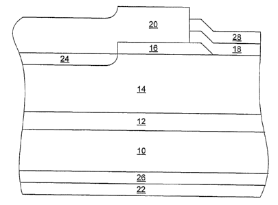
Figure 1 illustrates a first embodiment of a Schottky rectifier having
epitaxial
edge termination according to the present invention. A first (optional)
epitaxial layer
12 of n-type conductivity is grown on a single crystal bulk silicon carbide
substrate 10
of n-type conductivity and may act as a buffer layer. The first epitaxial
layer of silicon
carbide 12 is disposed between the substrate 10 and an n-type epitaxial layer
14 which
may provide a voltage blocking layer. The silicon carbide substrate 10 may be
an n+
9
CA 02425787 2003-04-09
WO 02/45177
PCT/US01/47924
SiC substrate, the first epitaxial layer 12 may be a highly doped n-type SiC
epitaxial
layer and the n-type epitaxial layer 14 may be a lightly doped n-type SiC
epitaxial
layer. Thus, the first epitaxial layer 12 may have a carrier concentration
comparable
to the silicon carbide substrate 10 and the n-type epitaxial layer 14 may have
a lower
carrier concentration than the silicon carbide substrate 10. A Schottky
contact 18 is
also provided on the n-type epitaxial layer 14.
A p-type silicon carbide epitaxial termination region 16 is also provided. The
p-type epitaxial termination region 16 is provided on the n-type epitaxial
layer 14 and
is adjacent the Schottky contact 18. A passivating oxide 20 may also be
provided.
The passivating oxide 20 may cover exposed areas of the Schottky rectifier
other than
the Schottky contact 18. Furthermore, an ohmic contact 22 may also be provided
on
the substrate 10 opposite the Schottky contact 18. The ohmic contact 22 may be
provided on an optional n+ region of silicon carbide 26 which may be provided
by
implantation in the substrate 10 and/or as an epitaxial layer formed on the
substrate
10. Preferably, the p-type epitaxial termination region 16 extends from the
Schottky
contact 18 a distance from about 2 to about 3 times the thickness of the n-
type
epitaxial layer 14. The silicon carbide substrate and epitaxial layers may be
4H SiC.
Figure 1 also illustrates an optional n+ region of silicon carbide 24 in the n-
type voltage blocking layer 14 at the periphery of the p-type epitaxial
termination
region 16. The n+ region of silicon carbide 24 may provide a "channel stop"
region
for the Schottky rectifier. An optional metal overlayer 28 on the Schottky
metal 18 is
also illustrated in Figure 1.
In particular embodiments of the present invention, the p-type epitaxial
termination region 16 has a controlled doping and thickness so as to provide a
predefined charge in the p-type epitaxial termination region 16 based on the
surface
doping of the n-type voltage blocking layer 14. Preferably, the charge in the
p-type
epitaxial termination region 16 is selected based on a theoretical optimum
junction
termination extension (JTE) charge given the surface doping concentration of
the
epitaxial layer used to make this structure:
QJTE, act = OCOJTE,opt, where
=(er x sox Ec)
0
¨,JTE,opt
where:
a is a proportionality value between 0.5 and 1.0;
CA 02425787 2010-03-01
. =
QJTE,opt is the theoretical optimum JTE charge;
81- is the relative dielectric constant of SiC (which is about 9.7);
co is dielectric constant of air which is 8.854x10⁻¹⁴c-cm/V;
Ec is the critical electric field of SiC, which is dependent on the doping by
the
formula given below;
q is the electronic charge which is 1.602x10⁻¹⁹ C; and
QJTE,act is the actual selected JTE charge.
The critical electric field of SiC is given by the following equation:
249 x10'
Ec = ______________ ,Vican;
(1 - 0.25 x logio(N/101")
where N is the doping of the n-type blocking layer. See "Ionization rates and
critical
fields in 4H-SiC", by A.0 Konstantinov, Q. Wahab, N. Nordell and U. Lindefelt,
Applied Physics Letters, vol. 72, No. 1, July 1997.
An illustration of the relationship of JTE charge to surface doping is seen in
Figure 3A. The line identified as "theoretical" corresponds to an a of 1.0 and
the
"75% theoretical" line corresponds to an a of 0.75. Figure 3B shows an
exemplary
illustration of the relationship of the "ideal" blocking voltage VB to surface
doping ND
in the voltage blocking layer 14 for a range of given thickness WE, of the
voltage
blocking layer 14. In this context "ideal" refers to the best blocking voltage
obtainable for a given layer thickness and doping without regard to surface or
other
effects. Figure 3B shows that, as the surface doping ND in the voltage
blocking layer
14 increases, the ideal blocking voltage generally decreases. In general, the
ideal
blocking voltage VB may be calculated using the following equation:
V =fi(wDxEc)
2
where 0.75 1 and Ec is given by the equation set forth
above. A doping level in
the range of lx1015to 2x10¹⁶ may yield a blocking voltage from approximately
2.5 kV
at wc. = 30 iirn to 400 V at wr, = 4 um, provided the doping is selected to be
as high as
possible while keeping the device in the punch-through regime.
As those of skill in the art will recognize, a diode epitaxial design is said
to be
in the punch-through regime when the breakdown voltage is primarily a function
of
the epitaxial thickness of the voltage blocking layer. In contrast, in the non-
punch-
through regime, the breakdown voltage is primarily a function of doping. For a
given
11
CA 02425787 2003-04-09
WO 02/45177
PCT/US01/47924
epitaxial thickness, whether a diode design is in the punch-through regime or
non-
punch-through regime depends on the doping of the voltage blocking layer. In
general, an empirical relation describing the boundary between the punch-
through
regime and the non-punch-through regime may be:
BV=5.73x10¹⁴N6. 33.
An exemplary illustration of the blocking voltage to JTE charge (QTTE) is
shown in Figure 3C. As seen in Figure 3C, as charge in the JTE increases for a
given surface doping of the blocking layer, the breakdown voltage of the
device
generally increases. However, if surface doping of the blocking layer remains
constant and charge increases beyond a threshold value (identified in Figure
3C as
QJTE,opt), the blocking voltage of the device decreases: Furthermore, the
absolute
value of the slope of the curve of blocking voltage versus JTE charge is
substantially
greater above the threshold value than below. This maximum point in the
blocking
voltage versus JTE charge curve is the "theoretical optimum" charge as it is
the
charge which theoretically provides the maximum breakdown voltage of a device
for
a give voltage blocking layer surface doping. Because the slope is steeper
above the
theoretical optimum value, it may be preferable to avoid exceeding the
theoretical -
optimum value. Thus, it is preferable the a value not be substantially greater
than
1Ø Furthermore, if a is too small, then the JTE may have only limited effect
on the
performance of the device. Thus, it is preferred that a be greater than about
0.5.
Additionally, because exceeding the optimum charge value may substantially
decrease the blocking voltage of the device, it is preferred that variations
in the
manufacturing process(es) be taken into account in establishing the charge for
the
JTE. Thus, it may be preferable to utilize an a value of about 0.75 or from
about 0.75
to about 1Ø However, as will be appreciated by those of skill in the art in
light of the
present disclosure, the selection of an a value may depend on the degree of
variation
in the final products, the acceptable failure rate or other manufacturing
concerns.
FIGs. 2A through 21 illustrate processing steps which may be utilized in
producing Schottky rectifiers having edge termination according to various
embodiments of the present invention. As seen in Figure 2A, a layer of n+
silicon
carbide 12 may optionally be formed on a single crystal silicon carbide
substrate 10
by epitaxial growth, ion implantation or other such techniques known to those
of skill
in the art. An ri epitaxial layer of silicon carbide 14 is formed on the n+
silicon
12
CA 02425787 2003-04-09
WO 02/45177
PCT/US01/47924
carbide layer 12 if present, or the substrate 10. The ri" epitaxial layer 14
may also be
formed utilizing techniques known to those of skill in the art.
As illustrated in Figure 2B, a p-type epitaxial layer is formed on the n-
epitaxial layer 14 with a doping and depth which are controlled so as to
provide the
predetermined charge proportional to the surface charge of the if epitaxial
layer 14 as
described above. Such a doping and depth may also take into account any loss
in the
p-type epitaxial layer during subsequent processing so that the final p-type
termination region has the proper final total charge.
Figure 2C and 2D illustrate optional processing steps for providing channel
stop implants. As seen in Figure 2C, a masking oxide 42 is formed on the p-
type
epitaxial layer 40. Such a masking oxide may be formed, for example, utilizing
Plasma Enhanced Chemical Vapor Deposition (PECVD) of Si02. The p-type
epitaxial layer 40 and the masking oxide 42 are then patterned so as to
provide an
oxide mask 42' and a patterned p-type layer 40' for implantation of the
channel stop
24. Furthermore, the opposite surface of the substrate 10 may also be
implanted with
n-type dopants so as to provide an optional n+ layer 26' suitable n-type
dopants may
include Nitrogen and Phosphorous. The structure of Figure 21) may then be
annealed
to activate the n-type implants. Optionally, such an anneal may be delayed and
performed simultaneously with the thermal oxidation of the p-type layer 40' as
described below. Techniques for implantation and activation of n-type dopants
in SiC
are known to those of skill in the art. In the event that one or more of the n-
type
implants are not incorporated in the device, then the implant and/or annealing
step(s)
may be omitted. However, it is preferred that the patterning of the p-type
layer 40
still be carried out so as to define the outer periphery of the p-type
epitaxial
termination region 16.
As is seen in Figure 2E, after removal of the oxide mask 42', a passivating
oxide layer 44 is formed on the exposed surface of at least the patterned p-
type
epitaxial layer 40', the n-type implanted region 24 (if present) and/or the n-
type
voltage blocking layer 14. If an n-type implant is also provided in the
opposite face of
the substrate, then an oxide layer 50 may also be deposited on the opposite
side of the
substrate 10 over the implanted region 26'. Such oxide layers may help to
prevent
loss of ion implanted regions during subsequent thermal oxidation steps.
Preferably,
the oxide layers 44 and 50 are deposited oxide layers and more preferably are
Low
13
CA 02425787 2003-04-09
WO 02/45177
PCT/US01/47924
Pressure Chemical Vapor Deposition (LPCVD) layers of Si02, however, high
quality
Plasma Enhanced Chemical Vapor Deposition 9PECVD) may also be used.
As illustrated in Figure 2F, the oxide passivating layer 44 may be patterned
to
expose the p-type layer 40'. Such a patterning may be accomplished by
photolithography and reactive ion etching, selective growth or other such
techniques
known to those of skill in the art. The oxide passivating layer 44 is
preferably
patterned so as to provide a window for formation_of the Schottky contact so
as to
provide a passivating layer 20 on exposed portions of the final device other
than the
Schottky contact 18. The structure of Figure 2F is thermally oxidized for a
time
' 10 sufficient to completely oxidize the exposed portion of the p-type
layer 40' so as to
provide a region of oxidized p-type SiC 46 corresponding to the Schottky
contact
location and the termination region 16 as is seen in Figure 2G. Such a thermal
oxidation is preferably carried out in a dry ambient of preferably less than
about 1500
. C and more preferably about 1300 C or less for a time sufficient to
completely
oxidize the p-type epitaxial layer 40'. The duration of such a thermal
oxidation may
vary depending on the temperature utilized and the thickness of the p-type
epitaxial
layer 40'. As described above, such thermal oxidation step may also be
utilized to
activate the n-type implants.
After the thermal oxidation is complete, the oxide layer 50 is removed from
the opposite side of the substrate by, for example, reactive ion etching, and
a metal
layer deposited to provide an ohmic contact 22. Suitable materials for such an
ohmic
contact include Nickel or other such materials known to those of skill in the
art. The
metal layer is also annealed to form the ohmic contact 22. The anneal may be
accomplished by a rapid thermal anneal process. Such operations are
illustrated by
Figure 211. After forming the ohmic contact 22, a photoresist pattern is
deposited to
provide a window for making the Schottky contact 18 and the thermal oxide
etched
through to the n-type epitaxial layer 14 so as to provide the window for
forming the
Schottky contact 18. Such an etch of the oxide 46 may be accomplished by a
buffered
oxide etch. As seen in Figure 21, the Schottky metal is deposited in the
window
formed by the etching of the oxide region 46 and may slightly overlap the p-
type
termination region 16. The Schottky metal may be any suitable Schottky metal,
such
as Nickel, Chromium, Titanium or Platinum. Also, an optional metal overlayer
28 of,
for example, gold, may be formed on the Schottky contact 18.
14
CA 02425787 2003-04-09
WO 02/45177
PCT/US01/47924
As illustrated in Figure 21, the Schottky contact 18 and the p-type edge
termination region 16 form a non-ohmic contact. Such a non-ohmic contact may
be
characterized by a non-linear voltage/current relationship of the contact. In
particular,
the contact has a finite turn-on voltage and a reverse leakage current which
is at least
103 times smaller than the rated on-state current. A reverse blocking voltage
is also
exhibited which is primarily determined by the epitaxial layer (14)
properties. In
addition, this junction follows closely the thermionic current transport
physics at room
temperature.
Figure 4 illustrates a further embodiment of the present invention where a
Junction Barrier Schottky (JBS)/ Merged P-I-N Schottky (MPS) grid 17 is
provided in
the Schottky gate region. A Schottky contact 18' and metal overlayer 28' may
be
provided over the JBS/MPS grid 17. Such a grid may be provided by modifying
the
patterning of the passivating layer 44 so as to provide a mask for oxidation
of the p-
type epitaxial layer 40' which provides the "bumps" or "islands" of the
JBS/MPS gate
structure illustrated in Figure 4. The oxide on the grid 17 may be removed by
mask
and reactive ion etching. Additionally, the grid 17 may be masked when the
thermally oxidized regions are etched away to provide the Schottky contact
window.
In the drawings and specification, there have been disclosed typical preferred
embodiments of the invention and, although specific terms are employed, they
are
used in a generic and descriptive sense only and not for purposes of
limitation, the
scope of the invention being set forth in the following claims.