Note: Descriptions are shown in the official language in which they were submitted.
CA 02426016 2003-04-14
WO 02/48740 PCT/SE01/02629
DETECTION OF RADIATION AND POSITRON EMISSION TOMOGRAPHY
TECHNICAL FIELD OF THE INVENTION
The present invention generally relates to detection of ionizing
radiation such as e.g. gamma and X-rays, and particularly to
positron emission tomography (PET).
More specifically, the invention relates to a novel detector
arrangement and a method, respectively, for highly temporally
and spatially resolved detection of radiation, and to a positron
emission tomography apparatus and a method, respectively, for
construction of an image of an object of interest from linear
projections of radiation as emitted from the object and
subsequently detected at high speed and at accurately determined
positions.
DESCRIPTION OF RELATED ART AND BACKGROUND OF THE INVENTION
A PET detector or camera typically consists of a polygonal or
circular ring of radiation detection sensors placed around a
patient area. Radiation detection begins by injecting isotopes
with short half-lives into a patient's body placed within the
patient area. The isotopes are absorbed by target areas within
the body, and emit positrons. In the human body, the positrons
annihilate with electrons. As a result thereof two essentially
monoenergetic gamma rays are emitted simultaneously in opposite
directions. In most cases the emitted gamma rays leave the body
and strike the ring of radiation detectors.
The ring of detectors includes typically an inner ring of
scintillation crystals and an outer ring of light detectors,
e.g. photomultiplier tubes. The scintillation crystals respond
to the incidence of gamma rays by emitting a flash of light
(photon energy), so-called scintillation light, which is then
converted into electronic signals by a corresponding adjacent
CA 02426016 2003-04-14
WO 02/48740 PCT/SE01/02629
2
photomultiplier tube. A computer, or similar, records the
location of each light flash and then plots the source of
radiation within the patient's body by comparing flashes and
looking for pairs of flashes that arise simultaneously and from
the same positron-electron annihilation point. The recorded data
is subsequently translated into a PET image. A PET monitor
displays the concentration of isotopes in various colors
indicating level of activity. The resulting PET image then
indicates a view of neoplasms or tumors existing in the
patient's body.
Such detector arrangement is known to have a good energy
resolution, but relatively bad spatial and temporal resolutions.
Early PET detectors required a single photomultiplier tube to be
coupled to each single scintillation crystal, while today, PET
detectors allow a single photodetector to serve several
crystals, see e.g. US Patents No. 4,864,138; 5,451,789; and
5,453,623. In such manner the spatial resolution is improved or
the number of photodetectors needed may be reduced.
Nevertheless, relatively low spatial resolutions are still
obtained. by PET detectors employing scintillator-based
photodetectors. Further improved spatial resolution requires the
use of a large number of small photodetectors and a scintillator
system, which generates light photons only in the scintillator
segment in which the incident radiation was absorbed. The use of
a larger number of photodetectors in a large array or to
increase the resolution of the device results in very complex
and expensive apparatus if at all realizable.
Further, in medical applications where it is desired to expose
the patient to a minimum amount of ionizing, it is important
that the detector device is sensitive to low levels of radiation
while still being able to discriminate against background
radiation. In some applications scintillator-based detectors may
CA 02426016 2003-04-14
WO 02/48740 PCT/SE01/02629
3
not possess sufficiently high sensitivities or signal-to-noise
ratios.
Still further, the light detecting arrangement of the detector
device is typically sensitive to direct irradiation by the
incident radiation and in such instance measures have to be
taken in order to prevent the incident radiation from reaching
such arrangement.
SUN~~ARY OF THE INVENTION
Accordingly, it is an object of the present invention to provide
a detector arrangement and method for detection of radiation,
which simultaneously provide for very high temporal and spatial
resolutions.
A further object of the invention is to provide a positron
emission tomography (PET) apparatus and a method, respectively,
for construction of an image of an object of interest from
linear projections of radiation as emitted from the object and
subsequently detected, which provide for a high speed and a very
high spatial resolution of the image constructed.
Yet a further object of the invention is to provide such
detector arrangement, PET apparatus, and methods, which provide
for effective rejection of noise; thus exhibiting high signal-
to-noise ratios.
Still a further object of the invention is to provide such
detector arrangement, PET apparatus, and methods, which provide
for spectrally resolved detection. In the case of PET detection
an improved energy resolution can provide for a lower number of
erroneously correlated signal pairs.
Yet a further object of the invention is to provide such
detector arrangement, PET apparatus, and methods, which can
CA 02426016 2003-04-14
WO 02/48740 PCT/SE01/02629
4
operate at fairly high radiation fluxes and which thus provide
for rapid examinations.
Still a further object of the invention is to provide such
detector arrangement, PET apparatus, and methods, which are
effective, accurate, reliable, easy to use, and of low cost.
These objects among others are, according to the present
invention, attained by detector arrangements, PET apparatus, and
methods, as claimed in the appended claims.
By providing a dual detector arrangement having a chamber filled
with a scintillating and ionizable substance wherein light as
well as electrons are created as a result of interactions
between incident radiation and the substance, and in which the
light and the electrons, respectively, are independently
detected in a respective arrangement detector, i.e. in a light
detector and in an electron avalanche detector, respectively,
followed by correlation of the respective light and electrons
which originate from the respective same incident radiation
photon, detection may be performed which exhibit major
advantages of both light detectors and electron avalanche
detectors. Particularly, as light detectors are known to provide
high energy resolution and electron avalanche detectors are
known to provide high position and temporal resolutions, the
inventive dual detector arrangement can provide the high energy
resolution of the light detectors and simultaneously provide the
high position and temporal resolutions of the electron avalanche
detectors.,Such detector arrangement is eminently adapted to be
employed in positron emission tomography (PET) to reject
otherwise erroneously matched signal pairs, by means of which
images with reduced levels of noise can be produced.
Further characteristics of the invention and advantages thereof
will be evident from the following detailed description of
CA 02426016 2003-04-14
WO 02/48740 PCT/SE01/02629
preferred embodiments of the invention, which are shown in the
accompanying drawings.
BRIEF DESCRIPTION OF THE DRAWINGS
The present invention will become more fully understood from the
5 detailed description of embodiments of the present invention
given hereinbelow and the accompanying Figs. 1-5, which are
given by way of illustration only, and thus are not limitative
of the invention.
Fig. 1 illustrates schematically, in a perspective view, a
radiation detector arrangement according to a first embodiment
of the present invention.
Fig. 2 illustrates schematically, in a cross sectional view, the
radiation detector arrangement of Fig. 1.
Fig. 3 illustrates schematically, in a perspective view, an
apparatus for positron emission tomography (PET) according to a
further illustrated embodiment of the present invention.
Fig. 4 illustrates schematically, in a cross sectional view, the
PET apparatus of Fig. 3.
Fig. 5 illustrates schematically, in a cross sectional view, a
PET apparatus according to yet a further embodiment of the
invention.
DETAILED DESCRIPTION OF PREFERRED EMBODIMENTS
In the following description, for purposes of explanation and
not limitation, specific details are set forth, such as
particular techniques and applications in order to provide a
thorough understanding of the present invention. However, it
will be apparent to one skilled in the art that the present
invention may be practised in other embodiments that depart from
these specific details. In other instances, detailed
CA 02426016 2003-04-14
WO 02/48740 PCT/SE01/02629
6
descriptions of well-known methods and apparatuses are omitted
so as not to obscure the description of the present invention
with unnecessary details.
With reference to Figs. 1 and 2, which schematically illustrate
in a perspective view and a cross sectional view, respectively,
a radiation detector arrangement 10, a first embodiment of the
present invention will be described.
Detector arrangement 10 includes a substantially planar cathode
13 and anode 35, respectively, and sidewalk 12 (which are
partly removed in Fig. 1 for illustrative purposes), which
together define a gas tight space or chamber 11 wherein an
ionizable and scintillating substance can be arranged. Cathode
13 also constitutes a radiation entrance window for incident
radiation, which typically may be gamma or X-rays, and is
typically oriented such that the incident radiation is entering
arrangement 10 substantially perpendicular to the plane of
cathode 13.
The ionizable and scintillating fluid, which preferably also
shall be a suitable medium for electron avalanche
multiplication, can be in gaseous, liquid, or solid phase and
comprises typically any of Ar, Xe, Kr, or a mixture thereof,
optionally with small amounts of e.g. C02, CH4, C2H6 or
isobuthane added thereto, to improve the avalanche amplification
achievable. If a gas or gas mixture is employed, it may be under
pressure, preferably in a range of 1-20 atm. If a solid is
employed it is preferably a solidified noble gas.
Cathode 13 includes a conductive cathode layer 33 optionally
carried by a dielectric substrate 34, and anode 35 includes a
plurality of rectangular, quadratic or otherwise shaped
conductive pads 39 arranged on a dielectric substrate 40. The
anode 35 also constitutes a readout arrangement of the detector
arrangement 10 and thus conductive pads 39 constitute readout
CA 02426016 2003-04-14
WO 02/48740 PCT/SE01/02629
7
elements for spatially resolved detection of electrons (created
as a result of ionization of the substance by the incident
radiation) drifted and accelerated towards the anode 35. The
conductive elements 39 are thus electrically insulated from each
other by means of the dielectric substrate 40.
Alternatively, a separate readout arrangement is provided which
may be arranged in vicinity of anode 35, in vicinity of cathode
13, or elsewhere. Typically, such readout arrangement is
separated from any adjacent electrode by means of a dielectric,
or similar. Some readout arrangement geometries to be used in
the present invention are further described in our copending
Swedish patent application No. 9901325-2 entitled Radiation
detector, an apparatus for use in planar radiography and a
method for detecting ionizing radiation and filed on April 14,
25 1999, which application hereby is incorporated by reference.
Further, the readout arrangement is connected to a signal-
processing device (not illustrated) for necessary and/or desired
post-processing of collected signal data. Preferably, the
readout elements 39 are separately connected to the signal
processing circuit by means of individual signal conduits. A
signal display unit (neither illustrated) is provided for
displaying the processed signal data.
Between and substantially in parallel with cathode 13 and anode
35 there is arranged an avalanche cathode 37, which typically is
a conductive sheet or similar provided with a plurality of holes
38, through which electrons may pass. Preferably holes 38 of
cathode 37 and readout elements 39 of anode 35 are aligned with
respect to each other such that each hole is overlying a
respective readout element.
Cathodes 13, 37 and anode 35 are held, during use, at selected
electric potentials by means of an electrical power supply
device (not illustrated). Preferably, anode 35 is grounded and
CA 02426016 2003-04-14
WO 02/48740 PCT/SE01/02629
8
cathodes 13, 37 are held at respective selected electrical
potentials such that a weak electrical field, called drift
field, is obtained substantially between cathode 13 and cathode
17 and a strong electrical field, called avalanche
multiplication field, is obtained between cathode 37 and anode
35, and possibly around cathode 37.
Other avalanche amplification arrangements that can be used as
an alternative to avalanche cathode 37 are further described in
our above mentioned Swedish patent application No. 9901325-2.
It shall particularly be noted that an ionizable and
scintillating solid material can be arranged between cathode 13
and cathode 37; and that another solid material, or fluid (gas
or liquid), which is suitable for electron avalanche
amplification, can be arranged between cathode 37 and anode 35.
The size of the detector arrangement and consequently of the
readout arrangement 35 may vary tremendously. In a large area
detector, such as would be used for medical imaging purposes, a
readout arrangement may typically have many thousands of readout
elements and have outer dimensions of up to 2 m x 2 m. At the
contrary thereto, a small area detector used for other
applications may be smaller than 1 mm x 1 mm.
Further detector arrangement 10 includes a light detector 17 for
detection of scintillating light emitted in space 11 as a result
of interactions between incident radiation and the substance.
Light detector 17 is preferably arranged so as to detect light
emitted mainly perpendicular to the incident radiation entered
into chamber 11 and includes typically an array of light
detecting elements 17a, such as e.g. photomultiplier tubes,
photodiodes, CCD elements or similar for independent detection
of light emitted in chamber 11.
Each of the light detecting elements may be provided with a
respective light collimator 21 such that each element "sees" a
CA 02426016 2003-04-14
WO 02/48740 PCT/SE01/02629
9
different portion of chamber 11. An alternative to the provision
of individual collimators for the light detecting elements is to
divide chamber 11 into a plurality of chamber sections separated
by light reflecting or absorbing walls (not illustrated), each
of the walls being substantially parallel with the incident
gamma or X-ray radiation such that each light detecting element
is capable of detecting light emitted within a single one of the
chamber sections.
In such manners each light detection element is capable of
detecting light derivable from absorption by a respective
transversely separated portion of the incident gamma or X-ray
radiation and thus one-dimensional imaging of the incident
radiation is provided.
An alternative light detector may comprise, as illustrated in
Fig. 2, the collimator 21, a photocathode 23, a protective layer
29, a space or chamber 31 to be filled with an ~avalanche
amplification medium, an avalanche amplifier or field
concentration device 25 housed within space 31, and a readout
arrangement 27, 28, the readout arrangement including an array
of readout elements 27 provided on a dielectric substrate 28 and
electrically connected to the signal processing device by means
of individual conduits (not illustrated). Such a detector for
detection of scintillating light is disclosed in our copending
Swedish patent application No. 0002079-2 entitled Radiation
detection apparatus and method, filed on June 05, 2000 and
hereby incorporated by reference, and operates in the following
manner.
Photocathode 23 is adapted to release photoelectrons in response
to the light emitted in chamber 11 and subsequently impinged
onto photocathode 23. The photoelectrons are preferably released
from a surface 23b (back surface) of photocathode 23 as a result
of the light impinging on an opposite surface 23a (front
surface) of photocathode 23. Further, the photoelectrons are
CA 02426016 2003-04-14
WO 02/48740 PCT/SE01/02629
drifted and accelerated towards avalanche amplifier 25 and
readout elements 27 by means of appropriately applied voltages
between photocathode 23 and avalanche amplifier 25 and between
avalanche amplifier 25 and readout elements 27, respectively.
5 Within and adjacent the avalanche amplifier, which may comprise
e.g. an electrode provided with apertures (similar to the
avalanche cathode 37 in chamber 11), the electrical field is
focused and as a result thereof the electrons are accelerated
and multiplied to release electron avalanches (due to repeated
10 collisions between electrons and the avalanche amplification
medium) . As these electron avalanches reach readout arrangement
27, 28 they are detected in one or several of the readout
elements 27.
Typically, the size of the individual light detecting elements
(PMT'S, photodiodes, readout elements etc.) of the light
detector 17 is larger or much larger than the size of the
readout elements 39 of the avalanche electron detector 13, 37,
35, such that the position resolution of light detector 17 is
worse or much worse than that of avalanche electron detector 13,
37, 35.
On the other hand light detectors are known to possess better
energy resolution than avalanche electron detectors do, and
light detector 17 in the present invention is designed and
optimized to possess as good energy resolution as possible.
Thus, the energy resolution of light detector 17 is better or
much better than that of the electron avalanche detector 13, 37,
35.
In operation, the detector arrangement 10 of Figs. 1 and 2 is
positioned in the path of the radiation, y or X-ray radiation,
desired to be detected. The radiation passes through cathode 13
and is absorbed in the substance housed within chamber 11. As a
result thereof scintillating light by is emitted and free
electrons e- are released (see Fig. 2). The scintillating light
CA 02426016 2003-04-14
WO 02/48740 PCT/SE01/02629
11
is detected by means of light detector 17 (e. g. as depicted
above), whereas the freed electrons are detected in the
following manner.
The applied electrical potentials are causing the freed
electrons (released from ionization through primary and
secondary reactions) to drift parallel with the electrical field
lines towards the avalanche cathode 37 and the anode 35.
Correspondingly produced positive charge carriers are drifted
with the electrical field lines towards the cathode 13.
At avalanche cathode 37 the electrons begin to be accelerated
due to the stronger electrical field experienced and they
interact with the substance, causing further electron-ion pairs
to be produced. Those produced electrons will also be
accelerated in the field, and will interact repetitively with
new materia, causing yet further electron-ion pairs to be
produced. This process continues during the travel of the
electrons in the avalanche region towards anode 35 located at
the bottom of the avalanche region, and in such manner electron
avalanches are formed.
These electron avalanches yield a very large and almost noise-
free amplification of the primary released electrons and induce
pulses in the readout elements 39, which amplified pulses are
individually detected as each readout element has its individual
signal conduit to the signal-processing device. The signal-
processing device processes then the pulses; it possibly shapes
the pulses, and integrates or counts the pulses from each
readout element. Correspondingly, the positive charge carriers
induce pulses that may be detected at the cathode 13, or
elsewhere.
Thus, by providing a two-dimensional array of readout elements
39 a detector arrangement 10 is obtained, wherein electrons
derivable mainly' from ionization by transversely separated
CA 02426016 2003-04-14
WO 02/48740 PCT/SE01/02629
12
portions of the incident radiation beam are separately
detectable. Hereby, the detector provides for two-dimensional
imaging.
The signal processing device, which may be a computer provided
with suitable software, includes a correlating means for
correlating light detected by light detector 17 and avalanche
amplified electrons detected by electron avalanche detector 13,
37, 35, which are derivable from a single radiation photon.
Hereby, the signals originating from the same incident radiation
photon in the two detector sections are identified and such
identification is performed for all signals if possible. Since
it is assumed that the light detector has fairly good energy
resolution and fairly bad spatial and temporal resolutions, and
the opposite holds for the avalanche electron detector section,
it is clear that the incident radiation flux limits the extent
to which all signals may be correlated or not. It is thus
appreciated that two incident radiation photons detected in the
avalanche electron detector section spatially and temporally
resolved have to be detected in the light detector section
either temporally or spatially resolved in order to determine
which signals in the respective detector sections that are due
to the same incident photon.
Further, the signal processing device comprises a producing
means for producing a single signal from two correlated signals,
i.e. correlated detected light (signal in the light detector)
and detected avalanche amplified electrons (signal in the
avalanche electron detector), where the produced signal is more
effectively detected against a noise background.
In such manner a detected signal is obtained which may be
superior to any of the individual signals obtainable using any
one of the detector sections. The inventive detector arrangement
may be useful in a large variety of fields such as e.g. the
medical field encompassing the techniques computerized
CA 02426016 2003-04-14
WO 02/48740 PCT/SE01/02629
13
tomography (CT), radiology, positron emission tomography (PET).
The invention may also be suitable to be used in non-destructive
testing; microscopy; and basic and applied research encompassing
e.g. detection of neutrons.
Further, the recorded signals carry spectral information of the
detected incident radiation photons and thus the detector
arrangement provides for energy resolved detection of radiation.
A similar detector apparatus based on a dual detector
arrangement for energy resolved radiation detection is disclosed
in our copending Swedish patent application No. 0003356-3
entitled Adaptable energy-resolved detectson ionizing radiation
and filed on September 20, 2000, which application is hereby
incorporated by reference.
As the light detector arrangement is known to provide a higher
energy resolution, the detector arrangement of the present
invention can be used to provide excellent spatial, temporal as
well as spectral resolution.
It shall be appreciated that while the embodiment described
above comprises a detector wherein the incident radiation is
intended to be entered into the detector through the cathode
thereof, there is no limitation whatsoever in this respect.
Particularly, the concept of the present invention is applicable
on a planar radiation detector, wherein the incident radiation,
which typically is a planar radiation beam, enters the detector
sideways between and substantially in parallel with the cathode
and anode, and wherein electrons released as a result of
ionization by said radiation is drifted and accelerated in a
direction which is substantially perpendicular to the direction
of the incident radiation. For a further detailed description of
such detector geometry, see our above-mentioned Swedish patent
applications No. 9901325-2 and No.0003356-3. The light
detection arrangement, which typically includes a linear array
of individual light detecting elements may be oriented and
CA 02426016 2003-04-14
WO 02/48740 PCT/SE01/02629
14
arranged to detect light emitted in a direction opposite or
substantially opposite to the direction of the drifted and
accelerated electrons, or to detect light emitted in a direction
parallel with the incident radiation. As regards other details
and features the arrangement may be configured and arranged as
in the Figs. 1-2 embodiment.
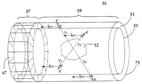
With reference now to Figs. 3 and 4, which illustrate
schematically, in a perspective view and in a cross sectional
view, respectively, an apparatus 50 for positron emission
tomography (PET), a particular applied embodiment of the present
invention will be briefly described.
PET apparatus 50 comprises a cylindrically shaped electron
avalanche detector section 59 and a light detector section 57
arranged at an axial end of detector section 59. Within the
electron avalanche detector section 59 a patient area is
arranged where a patient, or a portion thereof, 52 may be
placed. Electron avalanche detector section 59 comprises an
inner cylindrical cathode 53 transparent to gamma radiation and
an outer cylindrical anode 75, between which a suitable
electrical field is applied during operation by means of an
electrical power supply device (not illustrated).
Further, detector section 59 includes enclosure at the axial
ends thereof (not explicitly illustrated, but light detector
section 57 may provide enclosure at one of the ends) to define a
fluid tight annular space 51, wherein an ionizable and
scintillating fluid (or solid substance) can be arranged. The
ionizable and scintillating fluid, which preferably also is a
suitable medium for electron avalanche multiplication, may be
any of the substances or mixtures thereof as described in the
previous embodiment.
Anode 75 includes a plurality of separate electrically
conductive readout elements 79 arranged in a cylindrically
CA 02426016 2003-04-14
WO 02/48740 PCT/SE01/02629
shaped matrix, which readout elements 79 are preferably
rectangular, quadratic or have other shape and are electrically
insulated from each other. Such matrix of readout elements 79
is, as will be further described below, capable of providing
5 spatially resolved detection of electrons created as a result of
ionization of the fluid by gamma radiation entered through
cathode 53. Readout elements 79 as well as cathode 53 may be
arranged on respective dielectric substrates (not illustrated).
Further, light detector section 57 comprises a plurality of
10 individual light collecting elements 67 arranged in a circular
fashion to detect any scintillating light emitted in a
substantially axial direction. In the illustrated case sixteen
light detecting elements 67 are arranged to cover the complete
360° revolution of an axial end of annular space 51. The light
15 detecting elements are preferably PMT's, photodiodes, CCD
elements or other fast responding light detecting elements.
Detector elements that provide for measurements of high
intensity resolution are particularly preferable.
It shall be noted that the size of readout elements 79 is
smaller or much smaller than the size of light detecting
elements 67, which is shown in Fig. 4. As readout elements 79
are distributed over a cylindrically shaped surface, there are
provided a very high number of these compared with the number of
light detecting elements 67.
Radiation detection begins by injecting isotopes with short
half-lives into a patient's body 52 placed within the patient
area within the cylindrical detector section 59. The isotopes
are absorbed by target areas within the body, and emit
positrons. The positrons annihilate with electrons very fast. As
a result of each such annihilation two 511 keV gamma rays, yl~ 'y4
and y2; 'y3, are emitted simultaneously in opposite directions,
i.e. in directions separated by 180°. The emitted gamma rays
leave the body, penetrate through the cylindrically shaped
CA 02426016 2003-04-14
WO 02/48740 PCT/SE01/02629
16
cathode 53, and get absorbed by the ionizable and scintillating
fluid within annular space 51. As a result of each gamma ray
absorption scintillating light by is emitted isotropically and
free electrons e- are released.
The light by emitted substantially in an axial direction towards
the light detector 57 (denoted by arrows in Fig. 3) from each
absorbed gamma ray y1; y4 and y2; y3 is detected in a respective
one of the individual light detecting elements. The amplitude or
the integrated value of each light induced signal is a measure
of the energy of the corresponding radiation photon. Thus,
signals which do not lie within an acceptable spectral window
can be rejected. How this will be used in a novel manner is
described below.
The released electrons e- from each absorbed gamma photon are
caused to drift towards the cathode 75 and the matrix of readout
elements 79 thereof by means of the applied electrical field.
Correspondingly produced positive charge carriers are drifted
towards the cathode 53.
If the electrical field applied is sufficiently high the
electrons are heavily accelerated and interact with the fluid,
causing further electron-ion pairs to be produced. Those
produced electrons will also be accelerated in the field, and
will interact repetitively with new materia, causing yet further
electron-ion pairs to be produced. This process continues during
the travel of the electrons in the avalanche region towards
anode 75. It shall be noted that avalanche amplification may be
facilitated if a suitable field concentration means is arranged
between cathode 53 and anode 75.
Electrons impinging on readout elements 79 induce electrical
pulses therein, which are detected. Electrons resulting from
absorption of a single gamma photon are detected individually in
one or several readout elements 79. By providing a large amount
CA 02426016 2003-04-14
WO 02/48740 PCT/SE01/02629
17
of small and closely located readout elements 79 a good spatial
resolution is obtained.
Detection of two gamma photons simultaneously in two differently
located readout elements 79 indicates then an annihilation of a
positron in the patient along a straight line between these
elements.
A computer (not illustrated), or similar, records the location
of each of these projections and then plots the source of
radiation within the patient. The recorded data is subsequently
translated into a PET image. A PET monitor displays the
concentration of isotopes e.g. in various colors indicating
level of activity.
It shall be appreciated that when using such electron avalanche
detector 59 an improved spatial and temporal resolution may be
obtained to the cost of a deteriorated energy resolution. The
number of readout elements 79 in the inventive detector may be
very high (several thousands) without complicating or raising
the price of the detector and further they may be made very
small, e.g. in the submillimeter region.
However, as a consequence of the limited energy resolution of
such detector the energy information cannot easily be used for
rejection of background or noise. In order to improve the noise
rejection of the inventive high-resolution PET apparatus the
light detector 57 may be employed. By means of correlating
detected light and detected avalanche amplified electrons, which
are derivable from a single radiation photon pair, one signal
pair from said correlated detected light and detected avalanche
amplified electrons can be produced, where this produced signal
pair has spatial and temporal resolutions comparable to the
spatial and temporal resolutions of the detected avalanche
amplified electrons and an energy resolution better than the
spectral resolution of detected avalanche amplified electrons.
CA 02426016 2003-04-14
WO 02/48740 PCT/SE01/02629
18
Such correlation and signal production are repeated for each
detected light and each detected electron avalanche and thus an
image with lower levels of noise can be produced since the high
energy resolution of the light detector assists in rejecting
otherwise erroneously matched signals (i.e. signals that are not
of the predetermined energy 511 keV are rejected).
It shall be appreciated that the inventive PET apparatus may be
modified in a plurality of ways, not at least as regards size,
form and geometry.
Thus, in Fig. 5 is schematically illustrated a cross sectional
view of a PET apparatus according to a further embodiment of the
invention. Here, a triangular detector geometry is used instead
of the circular one illustrated in Figs. 3 and 4. Thus, three
planar dual detector arrangements 90 are arranged at an inclined
angle with respect to each other to define the triangular cross
sectional shape. Dual detector arrangements 90 are facing the
patient area and any patient, or similar, 52 placed therein.
Each detector 90 is similar to the one illustrated in Figs. 1
and 2, and comprises an electron avalanche detector section
including a planar matrix of readout elements 99 and a light
detector section including an array of light detecting elements
87.
Alternatively, more planar detectors are used to form a PET
apparatus, e.g. four to define a square or rectangular cross
section apparatus, or even further to define a polygonal cross
section apparatus.
It will be obvious that the invention may be varied in a
plurality of ways. Such variations are not to be regarded as a
departure from the present invention.