Note: Descriptions are shown in the official language in which they were submitted.
CA 02426183 2003-04-17
WO 03/017517 PCT/KR02/01575
-1-
APPARATUS AND METHOD FOR INTERFACING BETWEEN MODEM AND
MEMORY IN MOBILE STATION
BACKGROUND OF THE INVENTION
1. Field of the Invention
The present invention relates generally to an apparatus and method for
processing internal data in a mobile station (MS), and in particular, to an
apparatus and
method for interfacing between a modem and a memory.
2. Description of the Related Art
An MS serviced only voice calls in its earlier stage of development and now
supports a variety of services including data service along with users'
growing demands
and the advance of communication technology. The various services are a text
service, a
graphic service, E-mail, voice mail, navigation, transmission of moving
pictures, etc.
The MS is provided with a modem to process data received and data to be
transmitted over a wireless network. The modem is usually implemented in the
form of a
chip and the modem chip is essential to'driving the MS. The MS is also
provided with a
memory for storing data from the above services and information required to
operate the
MS. Therefore, the MS needs an apparatus for interfacing the modem and the
memory to
provide the above services.
A conventional MS uses a NOR flash memory for storing application programs
and OS (Operating System) codes. An interfacing structure between interfacing
data
between a modem and a memory in an MS using a NOR Flash memory is illustrated
in
FIG. 1.
Referring to FIG. 1, a chip select signal ROM_CSB, a read enable signal RDB,
a write enable signal WRB, an address signal A, and a data signal D are used
to interface
data between a modem 110 and a NOR flash memory 112. A chip select signal
(RAM CSB) is additionally used to interface between the modem 110 and a
working
memory 114.
Referring to FIG. 1, the modem 110 processes data received or data to be
CA 02426183 2003-04-17
WO 03/017517 PCT/KR02/01575
-2-
transmitted over a wireless network. Upon generation of data for data
transmission/reception over the wireless network, the modem 110 also stores
the data in
a NOR flash memory 112. The modem 110 reads data for transmission over the
wireless
network from the NOR flash memory 112. When the MS is powered-on, the modem
110
accesses basic codes required for initialization, such as boot codes, a vector
table, and
load codes through the NOR flash memory 112. The NOR flash memory 112 stores
application programs and OS codes needed in the MS. The working memory 114
temporarily stores application programs required for the modem 110 to process
predetermined data and provide a particular service, and can be accessed when
necessary.
The working memory 114 can be, for example, an SRAM or an UtRAM. For example,
after the initialization of the MS, the modem 110 reads the OS codes and a
call software
from the NOR flash memory 112 and copies them in the working memory 114. Then
the
modem 110 accesses the working memory 114. The reason for copying data from
the
NOR flash memory 112 to the working memory 114 is that data can be accessed
more
rapidly in the working memory 114 due to a short access time of the SRAM used
as the
working memory 114. The modem 110 reads or writes application data directly
from or
into the NOR flash memory 112. When necessary, the modem 110 copies the
application
data in the working memory 114.
To write data in the NOR flash memory 112, the modem 110 enables the NOR
flash memory 112 by the chip select signal ROM CSB, designates a predetermined
address by the address signal A during enabling the write enable signal WRB,
and
provides data to the NOR flash memory 112 by the data signal D at the same
time. The
NOR flash memory 112 is enabled by the chip select signal ROM_CSB and upon
receipt
of the address signal A and the data signal D for the period of enabling the
write enable
signal WRB, it stores the data represented by the data signal D in an area
designated by
the address signal A.
To read data from the NOR flash memory 112, the modem 110 enables the
NOR flash memory 112 by the chip select signal ROM_CSB and receives the data
signal
D from the NOR flash memory 112 by the address signal A during enabling of the
read
enable signal RDB. The NOR flash memory 112 is enabled by the chip select
signal
ROM CSB, reads data from a memory area designated by the address signal A
received
from the modem 110 during enabling of the read enable signal RDB, and
transmits the
data signal D to the modem 110.
CA 02426183 2003-04-17
WO 03/017517 PCT/KR02/01575
-3-
To write data in the working memory 114, the modem 110 enables the working
memory 114 by the chip select signal RAM_CSB and upon receipt of the address
signal
A and the data signal D during enabling the write enable signal WRB, it stores
the data
signal D representing data in a memory area designated by the address signal
A.
To read data from the working memory 114, the modem 110 enables the
working memory 114 by the chip select signal RAM_CSB and receives the data
signal D
from the working memory 114 by the address signal A during enabling the read
enable
signal RDB. The working memory 114 is enabled by the chip select signal RAM
CSB,
reads data from a memory area designated by the address signal A during
enabling of the
read enable signal RDB, and transmits the data signal D to the modem 110.
A memory capacity of 16 or 32Mbit is sufficient for services provided from an
MS at present. However, considering the rapid growth of the communications
market,
various MS services, advanced .functions, high capacity, and the resulting
increase in
data file size, a memory capacity requirement is 64/128Mbit or larger.
It is impossible to provide inexpensive NOR flash memories with an increased
memory speed requirement in view of its structure. Moreover, the drastically
growing
demands for NOR flash memories add to the difficulty with supplying parts for
manufacture of NOR flash memories. In this context, NAND flash memories may
become more widely used as memories for MSs because they can be provided at
cheap
prices.
In a comparison between a NOR flash memory and a NAND flash memory
with the same capacity, the former is 3.56 dollars per mega byte and the
latter is 0.83
dollars per mega byte. It is expected that the NOR flash memory and the NAND
flash
memory will be 3.06 and 0.6 dollars, respectively in 2002.
In terms of density, a NAND flash memory of 512 Mbit corresponds to a 64-
Mbit NOR flash memory is. In 2002, a NAND flash memory of 1024Mbit will
correspond to a 128-Mbit NOR flash memory.
It can therefore be concluded that the NAND flash memory is better than the
NOR flash memory in terms of cost and density. Therefore, NOR flash memories
have
CA 02426183 2010-09-30
-4-
reached their limits of use in MSs.
SUMMARY OF THE INVENTION
It is, therefore, an object of the present invention to provide an MS using a
NAND flash memory.
It is another object of the present invention to provide an apparatus and
method
for interfacing data between a modem and a NAND flash memory in an MS.
To achieve the above and other objects, there are provided an apparatus and
method for interfacing data between a modem and a NAND flash memory in an MS.
In
an interface circuit between the NAND flash memory and the modem, a working
memory has a capacity smaller than the capacity of the NAND flash memory,
copies part
of the information stored in the NAND flash memory therein, has second
addresses
different from the first addresses of the NAND flash memory. A programmable
memory
has basic codes required to copy the part of the information stored in the
NAND flash
memory to the working memory. A controller is connected to the programmable
memory, for controlling random reading of the information stored in the
working
memory using the second addresses.
To write data in the NAND flash memory, a write command is transmitted to the
NAND flash memory by enabling a second chip select signal for activating the
NAND
flash memory and a command latch enable signal when the modem enables a first
chip
select signal and the write command. A write address is transmitted to the
NAND flash
memory by disabling the command latch enable signal and enabling an address
latch
enable signal and writing data from the modem in the NAND flash memory. In
some
embodiments, an error correction code for the data is generated in an error
correction
code generator by disabling the address latch enable signal and a third chip
select signal.
The error correction code is transmitted to the NAND flash memory by disabling
the
third chip select signal and enabling the second chip select signal for
activating the
NAND flash memory, and written in the NAND flash memory. Then, the second chip
select signal is disabled.
In some embodiments, to read data from the NAND flash memory, a read
command is transmitted to
CA 02426183 2007-12-27
-5-
the NAND flash memory by enabling a second chip select signal for activating
the
NAND flash memory and a command latch enable signal when the modem enables a
first
chip select signal and the read command. A read address is transmitted to the
NAND
flash memory by disabling the command latch enable signal and enabling an
address
latch enable signal, and data at the read address and an error correction code
for the data
is read. An error correction code for the data is generated in the error
correction code
generator by disabling the address latch enable signal and a third chip select
signal.
When the third chip select signal is disabled, it is determined whether the
read data has
errors by comparing the read error correction code with the generated error
correction
code. If it is determined that the read data has errors, the errors are
corrected.
According to an aspect of the present invention there is provided an apparatus
for
interfacing, in a mobile station, between a NAND flash memory for storing data
and a
modem for processing data to be written in the NAND flash memory, comprising:
a memory controller for controlling data received from the modem and an error
correction code to be written in the NAND flash memory when a chip select
signal and a
write command are enabled;
a mask ROM (Read Only Memory) activated by the modem, for outputting basic
codes
required for initialization upon receipt of a read command from the modem at
initial
power-on; and
an error correction code generator activated by the memory controller, for
generating an
error correction code for data received from the modem and outputting the
error
correction code to the modem through the memory controller.
According to another aspect of the present invention there is provided a
method
of interfacing between a NAND flash memory and a modem in a mobile station
having
the NAND flash memory for storing data, the modem for processing data to be
written in
the NAND flash memory, the method comprising the steps of
transmitting a write command to the NAND flash memory by enabling a second
chip
select signal for activating the NAND flash memory and a command latch enable
signal
when the modem enables a first chip select signal and the write command;
transmitting a write address to the NAND flash memory by disabling the command
latch enable signal and enabling an address latch enable signal and writing
data from the
modem in the NAND flash memory; and
disabling the second chip select signal.
CA 02426183 2007-12-27
-5a-
According to a further aspect of the present invention there is provided a
method
of interfacing between a NAND flash memory and a modem in a mobile station
having
the NAND flash memory for storing data, the modem for processing data to be
written in
the NAND flash memory, and an error correction code generator for generating
an error
correction code for data received from the modem, the method comprising the
steps of:
transmitting a read command to the NAND flash memory by enabling a second chip
select signal for activating the NAND flash memory and a command latch enable
signal
when the modem enables a first chip select signal and the read command;
transmitting a read address to the NAND flash memory by disabling the command
latch
enable signal and enabling an address latch enable signal and reading data at
the read
address and an error correction code for the data;
generating an error correction code for the data in the error correction code
generator by
disabling the address latch enable signal and a third chip select signal;
determining whether the read data has errors by comparing the read error
correction
code with the generated error correction code; and
correcting errors if it is determined that the read data has the errors.
According to a further aspect of the present invention there is provided a
method
of interfacing between a NAND flash memory and a modem in a mobile station
having
the NAND flash memory for storing data, a programmable memory for having basic
codes to be read upon initialization from the NAND flash memory, a working
memory
having an address different from the NAND flash memory and the modem for
reading
data from the NAND flash memory, the method comprising the steps of:
initializing a modem on the basis of the basic data from the programmable
memory; and
reading a data from the NAND flash memory on the basis of the basic data and
writing
the read data in the working memory.
According to a further aspect of the present invention there is provided a
method
of interfacing between a NAND flash memory and a modem in a mobile station
having
the NAND flash memory for storing data, a programmable memory for having basic
codes to be read upon initialization from the NAND flash memory, an error
correction
code generator for generating error correction codes for a data
received/transmitted
between the modem and the NAND flash memory, a working memory having an
address
different from the NAND flash memory and the modem for reading data from the
NAND
flash memory, the method comprising the steps of:
+= CA 02426183 2009-09-29
r
-5b-
initializing a modem on the basis of the basic data from the programmable
memory; and
reading a data from the NAND flash memory on the basis of the basic data and
writing
the read data in the working memory.
BRIEF DESCRIPTION OF THE DRAWINGS
The above and other objects, features and advantages of the present invention
will
become more apparent from the following detailed description when taken in
conjunction
with the accompanying drawings in which:
FIG. I is a block diagram of a conventional apparatus for interfacing between
a
modem and memories in an MS;
FIG. 2 is a block diagram of an apparatus for interfacing between a modem and
a
memory unit in an MS according to an embodiment of the present invention;
FIG. 3 is a block diagram of an NFC (NAND Flash Controller) illustrated in
FIG. 2;
FIG. 4 is a flowchart illustrating data writing from the modem to the memory
unit
in the MS according to the embodiment of the present invention;
FIG. 5 is a flowchart illustrating data reading from the memory unit to the
modem
in the MS according to the embodiment of the present invention;
FIG. 6 illustrates part of a combination logic illustrated in FIG. 3;
FIG. 7 is a timing diagram for an interfacing apparatus having the combination
logic illustrated in FIG. 6;
FIG. 8 is a detailed circuit diagram of another embodiment of the combination
logic; and
FIG. 9 is a timing diagram for signals input to an ECC (Error Correction Code)
generator when the combination logic illustrated in FIG. 8 is used.
DETAILED DESCRIPTION OF THE PREFERRED EMBODIMENTS
CA 02426183 2003-04-17
WO 03/017517 PCT/KR02/01575
-6-
Preferred embodiments of the present invention will be described herein below
with reference to the accompanying drawings. In the following description,
well-known
functions or constructions are not described in detail since they would
obscure the
invention in unnecessary detail.
In order to replace a NOR flash memory with a NAND flash memory according
to the present invention, the following aspects are generally addressed.
(1) When an MS is initially power-on, a modem randomly accesses basic codes
including a vector table, boot codes, and load codes for initialization. In
the case of a
conventional NOR flash memory, it does not matter that the basic codes are in
the NOR
flash memory allowing random access. However, since a NAND flash memory
according to the present invention does not allow random access, a device for
allowing
random access to the basic codes is required
(2) A NAND flash memory controller is required, which controls the NAND
flash memory according to a command from the modem and reports the control
status of
the NAND flash memory to thereby enable the modem to access the NAND flash
memory.
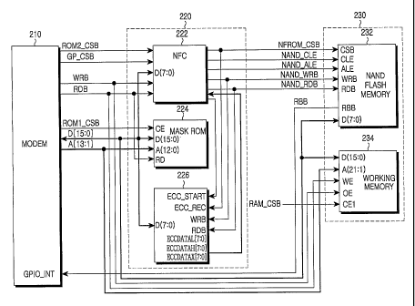
FIG. 2 illustrates an apparatus for interfacing between a modem and a memory
unit according to an embodiment of the present invention, which satisfies the
above
aspects. As illustrated, the interfacing apparatus is comprised of a modem
210, a
memory unit 230, and an interface 220 for interfacing between the modem 210
and the
memory unit 230.
Referring to FIG. 2, the interface 220 includes an NFC 222, a mask ROM
(Read Only Memory) 224, and an error correction code (ECC) generator 226. The
modem 210 can access the mask ROM 224 randomly. Therefore, the mask ROM 224
stores basic data required for initialization, such as a vector table, boot
codes, and load
codes, thereby obviating the need for a NOR flash memory or refresh. The basic
data of
mask ROM 224 is program data by which data is copied from a NAND flash memory
232 to a working memory 234.
The ECC generator 226 receives data transmitted between the modem 210 and
the memory unit 230 and generates a parity code ECCDATAL[7:0], ECCDATAH[7:0],
CA 02426183 2003-04-17
WO 03/017517 PCT/KR02/01575
-7-
and ECCDATAX[7:0] for the input data. The parity code is used for bit error
check and
correction in the modem 210. The mask ROM 224 is enabled by a chip select
signal
ROM1 CSB from the modem 210 and outputs data D[15:0] to the modem 210
according to an address signal A[13:1]. The NFC 222 controls the memory unit
230 so
that the modem 210 can write or read data in or from the memory unit 230. That
is, the
NFC 220 controls the memory unit 230 by signals NFROM CSB, CLE, ALE,
NAND WRB, and NAND RDB according to commands ROM2_CSB, GP_CSB, WRB
and RDB received from the modem 210. These signals and commands are described
further below. The NFC 220 also reports the current control status of the
memory unit
230 to the modem 210 and transmits a parity code generated from the ECC
generator
226 to the modem 210.
The memory unit 230 includes the NAND flash memory 232 and the working
memory 234. The NAND flash memory 232 writes or reads data under the control
of the
NFC 222. The working memory 234 temporarily stores data received from the
modem
210 to allow fast data access for the modem 210.
Now, signals related with the interface 220 will be defined below.
With regard to signals input to the interface 220, ROMl_CSB is a chip select
signal that enables the mask ROM 224. ROM2_CSB is a chip select signal input
to the
NFC 222 that is enabled when the NFC 222 accesses the ECC generator 226, the
NAND
flash memory 232, or the working memory 234. GP_CSB is a chip select signal
input to
the NFC 222 and enabled when the NFC 222 accesses the ECC generator 226 or the
NAND flash memory 232. A[13:1] is an address bus signal. RDB is enabled for
the
modem 210 to read data from the NAND flash memory 230, the working memory 234,
the ECC generator 226, or the NFC 222. WRB is enabled for the modem 210 to
write
data in the NAND flash memory 230, the working memory 234, the ECC generator
226,
or the NFC 222. D[15:0] is a data bus signal.
With regard to signals output from the interface 220, ALE (Address Latch
Enable Signal) is enabled to write an address in a data bus when the NAND
flash
memory 232 is accessed. CLE (Command Latch Enable Signal) is enabled to write
a
command in the data bus when the NAND flash memory 232 is accessed. The
command
can be defined according to the NAND flash memory 232. NFROM_CSB is a chip
CA 02426183 2003-04-17
WO 03/017517 PCT/KR02/01575
-8-
select signal enabled for the NFC 222 to access the NAND flash memory 232.
NAND WRB is enabled when the NFC 222 writes data in the NAND flash memory 232.
NAND_RDB is enabled when the NFC 222 reads data from the NAND flash memory
232.
With regard to internal signals in the interface 220, the NFC 222 enables the
ECC generator 226 by ECC_START to generate a parity code. ECC RCE is a chip
select signal enabled to read a parity code upon request from the NFC 222.
ECCDATAL[7:0], ECCDATAH[7:0], and ECCDTAX[7:0] are signals representing a
parity code generated from the ECC generator 226 upon request from the NFC
222.
Aside from the above signals, RBB is a signal representing the status of the
NAND flash memory, that is, a ready state or a busy state. The modem 210 is
not
allowed to access data when the NAND flash memory 232 is busy. In other words,
data
access is available only when the NAND flash memory 232 is ready. The modem
210
determines the current status of the NAND flash memory 232 by the signal RBB
received through a general purpose input/output pin GPIO INT for interfacing
the
modem 210 with external devices. RAM CSB is a chip select signal enabled when
the
modem 210 accesses the working memory 234. When the NFC 222 does not access
the
NAND flash memory 232, the signal ROM2_CSB can be connected to RAM_CSB.
Since basic codes for initialization are stored in the mask ROM 224, the modem
210 boots up using the basic codes read from the mask ROM 224 at initial power-
on.
After initialization, the modem 210 reads OS codes and a call software from
the NAND
flash memory 232 and copies them in the working memory 234. Then, the modem
210
accesses the working memory 234. The reason for copying data from the NAND
flash
memory 232 to the working memory 234 is the short access time of an SRAM or
UtRAM used as the working memory 234. While the modem 210 directly reads or
writes application data from or in the NAND flash memory 232, it can copy the
application data in the working memory 234 when necessary.
FIG. 3 is a detailed block diagram of the NFC 222 illustrated in FIG. 2.
Referring to FIG. 3, when the chip select signal GP_CSB and the write enable
signal
WRB received from the modem 210 are enabled and a particular address and data
are
written in the address bus signal A and the data bus signal D, respectively,
they control
CA 02426183 2003-04-17
WO 03/017517 PCT/KR02/01575
-9-
signals output through terminals QO to Q4 in a first register group.
Mux_Select is output
through the terminal Q3. If Mux Select is set to 0, the signals CLE, ALE,
NFROM CSB, NAND WRB, and NAND RDB related with the NAND flash memory
232 and the signal ECC RCE related with the ECC generator 226 are controlled
by a
first combination logic and the first register group. On the other hand, if
Mux Select is
set to 1, the signals CLE, ALE, NFROM CSB, NAND WRB, NAND RDB, and
ECC RCE are controlled by a second combination logic and a second register
group.
That is, the NAND flash memory 232 and the ECC generator 226 are controlled by
the
use of the first combination logic and the first register group, or the second
combination
logic and the second register group.
A description will be made below of the operation of the interfacing apparatus
according to the embodiment of the present invention. The operation can be
considered
in terms of data writing and data reading in and from the NAND flash memory
232.
FIGs. 4 and 5 are flowcharts illustrating control operations in the NFC 222
for
reading and writing data from and into the NAND flash memory 232,
respectively.
Referring to FIG. 4, the NFC 222 receives a data write request from the modem
210 in step 410. The modem 210 requests data writing using the address bus
signal A,
the data bus signal D, the write enable signal WRB, and the chip select signal
GP_CSB
or ROM2_CSB.
In step 412, the NFC 222 enables the chip select signal NFROM CSB for
accessing the NAND flash memory 232 and the signal CLE for transmitting a data
write
command to the NAND flash memory 232. The NAND flash memory 232 is enabled by
the NFROM CSB and prepares for receiving a command from the NFC 222 in
response
to the signal CLE. The NFC 222 transmits to the NAND flash memory 232 a write
command (80H) by the data bus signal D[7:0] in step 414. The NAND flash memory
232 then awaits receipt of an address and data to write. Meanwhile, the NFC
222
disables the signal CLE and enables the signals.NFROM CSB and ALE for
accessing
the NAND flash memory 232 and transmitting the address, respectively, in step
416.
In step 418, the NFC 222 transmits the address at which data is to be written
by
the data bus signal D[7:0]. The NFC 222 then disables the signal ALE and
enables the
CA 02426183 2003-04-17
WO 03/017517 PCT/KR02/01575
- 10-
signal ECC_START for generating a parity code in the ECC generator 226 in step
420.
The modem 210 transmits intended write data by the data bus signal D[15:0].
The data is written at the designated address in the NAND flash memory 232.
The data
is also fed to the ECC generator 226 and the ECC generator 226 generates a
parity code
ECDATAL[7:0], ECDATAH[7:0], and ECDATAX[7:0] for the received data.
The modem 210 enables the signal ECC_RCE through the NFC 222 to read the
parity code ECDATAL[7:0], ECDATAH[7:0], and ECDATAX[7:0] in step 422. The
NFC 222 disables the signal ECC_START and enables the signal NFROM CSB to
write
the parity code in the NAND flash memory 232 in step 424. Subsequently, the
modem
210 transmits the parity code by the data bus signal D[7:0] in step 426. The
parity code
is stored in a predetermined area of the NAND flash memory 232.
The NFC 222 enables the signal CLE in step 428 and transmits a check
command (10H) for determining whether the data writing is successful by the
data bus
signal D[7:0] in step 430. The NFC 222 disables the signal CLE in step 432.
Upon receipt of the check command, the NAND flash memory 232 transmits
information about its current status by a data bus signal D[6]. The current
status is a
busy state or an idle state. Even though it does not receive the check
command, the
NAND flash memory 232 always reports its current status to the modem 210 by
the
signal RBB. The NAND flash memory 232 notifies the NFC 222 whether the data
writing is successful by a data bus signal D[0].
The modem 210 determines the status of the NAND flash memory 232 by the
data bus signal D[6] or RBB in step 434. If the NAND flash memory 232 is in an
idle
state, the modem 210 determines whether errors have been generated during the
data
writing by the data bus signal D[0] in step 436. If the data writing is
successful, the NFC
222 disables the signal NFROM CSB and ends the data writing. On the other
hand, in
the case of a data writing failure, the NFC 222 disables the signal NFROM CSB
and
returns to step 410.
Referring to FIG. 5, the NFC 222 receives a data read request from the modem
210 in step 510. The modem 210 requests data reading using the address bus
signal A,
CA 02426183 2003-04-17
WO 03/017517 PCT/KR02/01575
-11-
the data bus signal D, the read enable signal RDB, and the chip select signal
GP_CSB or
ROM2_CSB.
In step 512, the NFC 222 enables the chip select signal NFROM CSB for
accessing the NAND flash memory 232 and the signal CLE for transmitting a data
read
command to the NAND flash memory 232. The NAND flash memory 232 is enabled by
the NFROM CSB and prepares for receiving a command from the NFC 222 in
response
to the signal CLE. The NFC 222 transmits to the NAND flash memory 232 a data
read
command (00H) by the data bus signal D[7:0] in step 514. The NAND flash memory
232 then awaits receipt of an address. Meanwhile, the NFC 222 disables the
signal CLE
and enables the signal ALE for transmitting the address in step 516.
In step 518, the NFC 222 transmits the address from which data is to be read
by
the data bus signal D[7:0]. The NFC 222 then disables the signal ALE in step
520. Upon
receipt of the data read command and the address, the NAND flash memory 232
transmits information about its current status by a data bus signal D[6] or
the signal RBB.
The current status is a busy state or an idle state. In the idle state, the
NAND flash
memory 232 reads data from the address and transmits it by the data bus signal
D[7:0].
The modem 210 determines the status of the NAND flash memory 232 by the
data bus signal D[6] or the signal RBB in step 524. If the NAND flash memory
232 is in
an idle state, the modem 210 enables the signal ECC_START for generating a
parity
code for the read data in step 524. The ECC generator 226 generates a parity
code
ECCDATAL[7:0], ECCDATAH[7:0], and ECCDATAX[7:0] for the read data.
The modem 210 reads the parity code from the ECC generator 226 by enabling
the signal ECC_RCE through the NFC 222 in step 526 and disables the signal
ECC_START through the NFC 222 in step 528. In step 530, the modem 210 reads a
parity code corresponding to the read data from the NAND flash memory 232.
Then the
modem 210 disables the signal NFROM CSB in step 532.
The modem 210 compares the generated parity code with the read parity code
in step 534 and determines whether the read data has errors according to the
comparison
result in step 536. If the parity codes are different, the modem 210
determines that the
read data has errors. If they are identical, the modem 210 determines that no
errors are in
CA 02426183 2003-04-17
WO 03/017517 PCT/KR02/01575
-12-
the read data.
If the modem 210 determines that the read data has no errors in step 536, it
ends
the data reading operation, and otherwise, it corrects errors in step 538 and
ends the data
reading operation.
As described above, data is written in a data area of the NAND flash memory
232. For the data writing, the ECC generator 226 generates a parity code for
the data.
The modem 210 writes the parity code in the NAND flash memory 232. In a data
reading operation, data read from the NAND flash memory 232 is fed to the ECC
generator 226. The ECC generator 226 generates a new parity code for the read
data.
The modem 210 compares the new parity code with a parity code corresponding to
the
read data, as stored in the NAND flash memory 232. According to the comparison
result,
the modem 210 determines whether the read data has errors. If it does, the
errors are
corrected.
Meanwhile, when power is initially on, the modem 210 reads the basic codes
from the mask ROM 224 to perform initialization. The initialization operation
will be
described with reference to FIG. 2.
At initial power-on, the modem 210 enables the chip select signal ROM1 CSB
to access the mask ROM 224. The mask ROM 224 is enabled by ROM1_CSB and
awaits a command from the modem 210. The modem 210 provides the mask ROM 224
with an address at which the basic data is stored by the address bus signal
A[13:1]. Then
the mask ROM 224 reads the basic codes at the address and transmits them by
the data
bus signal D[15:0]. The modem 210 performs initialization according to the
basic codes.
As stated before, the modem 210 copies data read from the NAND flash
memory 232 in the working memory 234, for fast access.
To do so, the modem 210 enables the chip select signal RAM_CSB to access
the working memory 234 via terminal CE1. If the modem 210 does not access the
NAND flash memory 232, the signal ROM2 CSB can be used instead of the signal
RAM CSB. The working memory 234 is activated by the signal RAM_CSB and awaits
receipt of a command from the modem 210. When the modem 210 intends to copy OS
CA 02426183 2003-04-17
WO 03/017517 PCT/KR02/01575
-13-
codes and a call software read from the NAND flash memory 232 in the working
memory 234, it enables the write enable signal WRB. On the contrary, to read
the OS
codes and the call software from the working memory 234, the modem 210 enables
the
read enable signal RDB. The signal WRB is fed to the working memory 234
through a
terminal OE and the signal RDB, to the working memory 234 through a terminal
WE.
When the terminal OE is enabled, the working memory 234 awaits receipt of an
address
and data such as OS codes, a call software, etc. from the modem 210. The
working
memory 234 receives the address by an address bus signal[21:1] and data by the
data bus
signal[15:0], and writes the data at the address.
If the working memory 234 is activated and then the terminal WE is enabled,
the working memory 234 awaits receipt of an address from the modem 210. Upon
receipt of the address by the address bus signal[21:1], it reads data at the
address and
transmits it to the modem 210 by the data bus signal D[15:0].
Referring back to FIG. 3, for the input of signals from the modem 210,
A[13:1],
D[15:0], GP_CSB, WRB, RDB, and ROM2_CSB, the NFC 222 outputs signals required
for data writing or data reading in or from the NAND flash memory 232, CLE,
ALE,
ECC_RCE, NFROM_CSB, GP_CSB_OUT, NAND_WRB, and NAND_RDB.
The signals GP_CSB and WRB are fed to a terminal CK of the first register
group through an AND gate. The first register group outputs the signal
Mux_Select
through the terminal Q3 as an enable signal for multiplexers (MUXes) that
multiplex the
signals CLE, ALE, ECC RCE, NFROM CSB, GP_CSB_OUT, NAND WRB, and
NAND RDB. The first register group controls the signals CLE, ALE, ECC RCE, and
NFROM CSB according to the signals A[13:0] and D[15:0] using the first
combination
logic. Signals A[12], and A[13] and the chip select signal GP_CSB are applied
to the
input of a second combination logic. The second combination logic generates
the signals
CLE, ALE, ECC RCE, and NFROM CSB. The signal GP_CSB OUT is used as an
interface signal for the NAND flash memory 232 or an LCD module (not shown).
When
the signal GP_CSB is enabled and both signals A[10] and A[13] are 1, the
signal
GP CSB OUT is enabled and used as a chip select signal.
FIG. 6 illustrates the second combination logic illustrated in FIG. 3.
Referring
to FIG. 6, the combination logic is constructed in the form of a flipflop
(F/F). A first
CA 02426183 2003-04-17
WO 03/017517 PCT/KR02/01575
L%,lIiif v 4 f U . U
-14-
inverter NOT1 inverts an address signal A[12]. A first OR gate OR1 OR-gates
the
output of the first inverter NOT1 and the chip select signal GP_CSB. A third
OR gate
OR3 OR-gates the output of the first OR gate OR1 and the write enable signal
WRB.
The output of the third OR gate OR3 is fed as a clock signal MSM_CLK to the
register
group-
A second inverter NOT2 inverts an address signal A[13]. A second OR gate
OR2 OR-gates the output of the second inverter NOT2 and the chip select signal
GP_CSB. A fourth OR gate OR4 OR-gates the output of the second OR gate OR2 and
the write enable signal WRB. A fifth OR gate OR5 OR-gates the output of the
second
OR gate OR2 and the read enable signal RDB. The outputs of the fourth and
fifth OR
gates OR4 and OR5 become a NAND flash memory write signal NAND WRB and a
NAND flash memory read signal NAND RDB, respectively.
FIG. 7 is a timing diagram for the NFC 222 having the combination logic
illustrated in FIGs. 3 and 6. With reference to FIG. 7, the timings of read
and write
signals will be described.
When data writing is requested, the chip select signal GP_CSB is enabled low
at time to. The signal WRB is enabled low for one clock period from the
falling edge of
time tl. This corresponds to transition from step 410 to step 412 in FIG. 4,
or from step
510 to step 512 in FIG. 5. That is, step 410 or 510 is satisfied since the
signals GP_CSB
and WRB are enabled. At time t2, the signal CLE is enabled high and the signal
NFROM CSB is transitioned to be low. That is, step 412 or 512 is performed.
Then
between the falling edge of time tl and the falling edge of time t7, a read
command or a
write command is output as an interface output I/O, as in step 414 or 514.
After the read
command or the write command is output, the signals CLE and ALE for enabling
transmission of the commands are both disabled at the falling edge of time t7.
Then, a read address or a write address is output. The ECC generator 226 must
be activated before writing data or reading data because of high error rate
during data
writing or data reading in or from the NAND flash memory.
To transmit a start command to the ECC generator 226, the signal GP_CSB is
enabled at the rising edge of time t8 and the signal WRB is enabled at the
falling edge of
CA 02426183 2003-04-17
WO 03/017517 PCT/KR02/01575
-15-
time t19. Therefore, at the falling edge of time t19, the signal NFROM_CSB
transitions
from low to high and the signal ECC RCE transitions from high to low. Thus
from time
t20 to time t25, the start command is delivered to the ECC generator 226.
Then, a data
read command or a data write command is executed.
As noted from FIG. 7, two clock pulses are lost before and after delivering a
command signal, respectively. It is because after the write clock signal
MSM_CLK is
generated using the address signal A[12] and the signal GP_CSB, it acts as a
flipflop
clock signal and thus produces the signals ALE, CLE, NFROM CSB, and ECC RCE
according to input data. In addition, with the address signal A[13] and the
signal
GP CSB, the signals NAND_WRB and NAND RDB are generated. Thus, the two-
clock pulse loss occurs before and after transmission of each command.
FIG. 8 is a detailed circuit diagram of another embodiment of the combination
logic according to the present invention. Referring to FIG. 8, the chip select
signal
GP_CSB is fed "to a first OR gate OR1, a second OR gate OR2, and a second
inverter
NOT2. The second inverter NOT2 inverts the signal GP_CSB. A first AND gate
AND1
AND-gates the address signal A[12] and the output of the second inverter NOT2
and
outputs a signal NAND _CLE. A second AND gate AND2 AND-gates the address
signal
A[11] and the output of the second inverter NOT2 and outputs a signal NAND
ALE.
Meanwhile, a first inverter NOT1 inverts the address signal A[13]. The first
OR
gate OR1 OR-gates the signal GP_CSB and the output of the first inverter NOT1
and
outputs a signal NAND_CSB. The second OR gate OR2 OR-gates the signal GP_CSB
and the address signal A[10] inverted in a third inverter NOT3 and outputs a
signal
ECC RCE.
FIG. 9 is a timing diagram for signals input to the ECC generator 226 in the
interface 220 having the combination logic illustrated in FIG. 8.
As compared to the signal timings illustrated in FIG. 7, no two-clock delay
occurs before and after delivery of a command signal utilizing the property of
the signal
GP_CSB. That is, it is because the signals ECC_RCE, ALE, CLE, and NFROM_CSB
are generated using signal pairs of GP_CSB and A[12], and GP CSB and A[13],
and
this combination logic does not utilize a flipflop.
CA 02426183 2003-04-17
WO 03/017517 PCT/KR02/01575
-16-
In accordance with the present invention as described above, a high-capacity,
cheap NAND flash memory substitutes for a NOR flash memory that imposes
constraints in terms of cost, capacity, and supply in an MS. Therefore, the MS
is
improved in cost and performance.
While the invention has been shown and described with reference to certain
preferred embodiments thereof, it will be understood by those skilled in the
art that
various changes in form and details may be made therein without departing from
the
spirit and scope of the invention as defined by the appended claims.