Note: Descriptions are shown in the official language in which they were submitted.
CA 02426314 2003-04-22
WO 02/35729 PCT/USO1/42815
1~~IETHOD AND APPARATUS rOR
SPACE DIVISION IV1ULTIPLE ACCESS
RL:CEIVER
rield of the Invention
The present invention relates to wireless communication networks, and morn
paI-ticularly to space-division multiple access (SUMA) in wireless
communication
networks.
Background of the Invention
Vfireless communication services are an increasingly common form of
conununication, and demand fur wireless services continuos to grow. Examples
of
wireless services include cellular mobile telephones, wireless Internet
service,
wireless local area computer networks, satellite communication networks,
satellite
television, and multi-user paging systems. Unfortunately, these communication
systems are conEned to a limited frequency spectrum either by practical
considerations or, as is often the case, by government regulation. As the
maximum
number of users, or "capacity," of these systems is reached, user demand for
more
service may be met by either ( 1) allocating more frequency spectrum to the
wireless
service, or (2) using the allocated frequency spectrum more efficiently.
Because the
frequency spectrum is limited and cannot keep pace with user demand, there is
a
~0 critical need for new technology that uses the allocated frequency spectrum
more
efficiently.
~t'ireless communication systems are generally composed of one ur more
base stations through which wireless users, such as mobile telephone users,
gain
access to a communications network, such as a telephone network. A base
station
~5 serves a number of wireless users, fixed ur nlubile, in a local area. To
increase the
capacity of the systems, service providers may install more base stations,
reducing
the area and the number of users handled by each base station. This approach
increases system capacity without allocating Inure spectrum frequency bands,
but is
quite costly because: it requires signiCcantly more hardware.
~U Alll7thCr appl'OaCh t0 L1S111~ the f1'ttluCllCy SpL'CtI-Lllll InOI'e C;
fllClt'ntly IS 1?f
improving "multiple access" icchnidues. Multiple access tcchnidues allwv
multiple
CA 02426314 2003-04-22
WO 02/35729 PCT/USO1/42815
_?_
users to share the allocated frequency spectrum so that they do not interfere
with
each other. The most common multiple access schemes are Frequency-Division
Multiple Access (FUMA), Time-Division Multiple Access ('TDMA), C.~ode-Division
Multiple Access (CDMA), and more recently Space-Division Multiple Access
(SDMA).
FDMA slices the allocated frequency band into multiple frccluency channels.
Each user transmits and receives signals on a different frequency channel to
avoid
interfering with the other users. When one user no longer requires the
frequency
channel assigned to it, the frequency channel is reassigned to another user.
With 'fDMA, users may share a common frequency channel, but each user
uses the common frequency channel at a different time. In other words, each
user is
allocated a time slot in which the user may transmit and receive. Thus, TDMA
interleaves multiple users in the available time slots.
CDMA allolvs multiple users to share a common frequency channel by using
coded modulation schemes. CDMA assigns distinct codes to each of the multiple
users. The user modulates its digital signal by a v=ideband coded pulse train
based
on its district code, and transmits the modulated coded signal. 'I°he
base station
detects the user's transmission by recognizing the modulated code.
In SDMA, a system may separate a desired user's signal from other signals
~0 by its direction of arrival, ar spatial characteristics. 'this is sometimes
referred to as
"spatial filtering." Thus, even though two users may be transmitting an the
same
frequency at the same time, the base station may distinguish them because the
transmitted signals from the users are arriving from different directions. It
is
possible to use SDMA in combination with FDMA, TDMA, or CDMA.
~5 A conventional SDMA receiver requires an array of multiple recc.?ive
elements. Further, a conventional SDMA receiver uses a bank of 1)hase shifters
that
cooperates with the receive element array to farm a'"beam" that "looks" in a
particular direction. It is generally hare desirable to farm multiple beams,
each
directed toward a different direction, 1.e., toward different users. The mare
beams,
3U the IIloI'e S1111L11taIleoLlS llSerS the SDMA Sy5teT11 Ina1' hallllle
optl'atlng an the Sallle
ll'ClllICIICy at thP. 5allle t1111t;. Thl', IIloI'P. bei1111S, hoV'ever, the'.
nloI'e CaI11p11Cated th('.
CA 02426314 2003-04-22
WO 02/35729 PCT/USO1/42815
-3-
SDMA receiver, For instance, each beam may require a separate bank of phase
shifters and circuits that perform signal tracking. Additionally, each beans
may
require a separate "signal combincr," which combines the signals received from
each
receive element to form a "combined signal." FuI-tller still, each combined
signal
may require a separate signal detector, which detects the transmitted signal
from the
user. This hardware complexity greatly increases the cost of an SDMA receiver.
Using well known algorithms, hardware complexity may be reduced by
performing phase shifting, signal tracking, signal combining and signal
detecting in
signal processing software. Current signal processing techniques, however,
have
difficulty identifying and tracking large numbers of simultaneously
transmitted
signals on the same frequency, paI-ticularly in a "multipathing" ~:nvironment.
A
multipathing environment is ogle where transmitted signals may reach the
receiver
over multiple paths. For instance, a transmitted signal may reach tile
receiver (1)
directly, and (2) indirectly after reflecting off objects. Multipath signals
may also
further complicate the complexity of the conventional SDMA receiver in the
same
manner as described above.
Thus, there is a need to provide an improved SDMA receiver that can
simultaneously receive from multiple directions and operate in a multipath
environment without likewise increasing hardware or software complexity of the
~0 receiver.
Summary of the Invention
The summary and the following detailed description should not restrict the
scope of the claimed invention. F3oth provide examples and explanations to
enable
others to practice the invention.
~5 Methods and systems consistent with this invention may incorporate a multi-
element receive signal array that may achieve polarization independent
isotropic
reception, with power gain that may be greater than isotropic. Such methods
and
systems may receive multiple signals having the same or different carrier
frequencies, distinguish the signals, and establish their dirc~cticlns of
arrival.
30 Methods and systems consistent with this invention receive a plurality of
tl'anSlllltted SlgnalS III a rf:CP.lver havlllg tl p1111'allty of I'ecClve
c'ltIlll;llt5, V'hcrl.'l11 each
CA 02426314 2003-04-22
WO 02/35729 PCT/USO1/42815
_:~_
transmitted signal has a different spatial location. Such methods and systems
receive the plurality of transmitted signals in the plurality of receive
elements to
form a plurality of receive element signals, form a combined signal derived
from the
plurality of receive element signals, and detect the plurality of transmitted
signals
from the combined signal by its different spatial location.
To achieve this, methods and systems consistent with this invention generate
a plurality of phase modulation signals that may be arbitrary or uncorrelated,
and
phase modulate each of the plurality of receive element signals with a
different one
of the phase modulation signals to form a plurality of phase modulated
signals.
Such methods and systems then combine the plurality of phase modulated signals
into a combined signal, generate expected signals, and correlate the combined
signal
with the expected signals to form correlation signals. Such methods and
systems
then store the con-elation signals in a correlation signal memory and analyze
the
correlation signals to extract information from the detected transmitted
signals.
Brief Description of the Drawings
The accompanying drawings, which are incorporated in and constitute a part
of this specification, illustrate an implementation of the invention and,
together with
the description, serve to explain the advantages and principles of the
invention. In
the drawings,
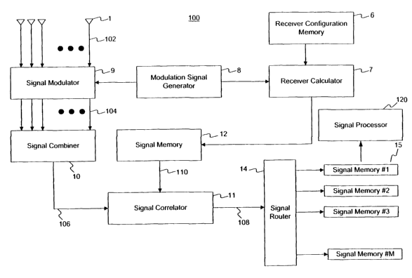
~U FIG. 1 is a block diagram, consistent with this inv ention, of a receiver;
FIG. 2 is a diagram of an environment, consistent with this invention, in
which the receiver of FIG. 1 may operate;
FIG. 3A is a diagram of phase modulation signals, consistent with this
invention generated by a modulation signal generator as shown in FIG. I;
FIG. 3B is a diagram of phase modulated signals generated by a signal
modulator as shown in FIG. l, and a combined signal, all consistent with this
invention; and
FIG. ~ is a flow chart of a process 4UU for space-division multiple access
receiving consistent with this iwention.
3U Detailed Description of the Invention
Overview
CA 02426314 2003-04-22
WO 02/35729 PCT/USO1/42815
_5_
The following description of embodiments of the present invention refers to
the accompanying drawings. Where appropriate, the same reference numbers in
different drawings refer to the same or similar elements.
Methods and systems consistent with this invention overcome the hardware
and software complexity of the conventional SDMA receiver in a wireless
system.
Such methods and systems comprise a receive element array with a plurality of
receive elements. Users of the wireless system transmit a plurality of
signals, each
signal having a different direction or spatial location relative to the
receive element
array. 'The users may be, for instance, mobile telephone users.
The receive element array receives the plurality of transmitted signals in the
plurality of receive elements to form a plurality of receive element signals.
Such
methods and systems form a single combined signal derived from the plurality
of
receive element signals, and nlay detect each of the plurality of transmitted
signals
from the single combined signal based upon its different spatial location.
Thus,
such methods and systems do not need multiple banks of phase shifters,
multiple
signal combiners, ur multiple signal detectors. Instead, such methods and
systems
may detect signals from multiple users based on their different spatial
location fi°om
a single combined signal, as opposed to forming a different combined signal
for
each signal from each user and detecting a signal from each combined signal.
?0 To achieve this, methods and systems consistent with this invention
generate
a plurality of phase modulation signals that nlay be arbitrary or uncorrelated
phase
modulation signals, and phase modulate each of the plurality of receive
element
signals with a different one of the phase modulation signals to form a
plurality of
phase modulated signals. Such methods and systems then combine the plurality
of
~5 phase modulated signals into the combined signal, generate expected
signals, and
correlate the combined signal with the expected signals to form correlation
signals.
The expected signals are the combined signals expected from the directions of
the
users, and may be a function of the phase modulation signals and the direction
of the
users. Such methods and systems then store the correlation signals in a
correlation
U Slgn~ll IIlelIlUry Gild allalyLe tlll,' ClarI'elatlull S1g17a1S tU eXt1'tlct
tllt', tl'a17S1711tt1;d
information in the signals from the users.
CA 02426314 2003-04-22
WO 02/35729 PCT/USO1/42815
-G-
Implementation Details
Methods and systems consistent with this invention receive a transmitted
signal in a receiver having a plurality of receive dements. FIG. 1 is a block
diagram
of a receiver 1 OU consistent with this invention. Receiver 100 comprises an
array 1
having a plurality of receive elements, a modulation signal generator 8, a
signal
modulator ), a signal combiner 10, a receiver configuration memory G, a
receiver
calculator 7, a signal memory 12, a signal correlator 1 l, a signal muter 14,
a
plurality of signal memories 15, and a signal processor 120. Receiver 100 may
include other components not specifically described above such as alters,
mixers,
amplifiers, and power supplies. The location of these components may vary
depending upon the preference of designers skilled in the an.
FIG. 2 is a diagram of an environment 200, consistent with this invention, in
which receiver 100 may operate. In environment 20D, remote transmitter A and
remote transmitter B may transmit signals 2 and 3, respectively from remote
transmitter space ''U?. Remote transmitters A and B may be mobile telephones,
for
example.
Transmitted signals 2 and 3 impinge un array I, and the plurality of elements
receive signals ? and 3 to form a plurality of receive element signals. The
plurality
of receive element signals are conveyed (via lines 102) to a signal modulator
J,
?0 which is described in detail below.
Methods and systems consistent with this invention generate a plurality of
phase modulation signals. Modulation signal generator $ generates phase
modulation signals fur the receive elements of array I . These phase
modulation
signals may be arbitrary or uncurrelated (correlation less than one). The
~5 uncorrelated phase modulation signals may be substantially un correlated or
only
slightly uncorrelated. For instance, the uncurrelated random please signals
may have
a correlation less than 1, but greater than 0.75; less than ur equal to 0.75,
but greater
than 0.50; less than ur equal to 0.50, but greater than D.25; less than ur
equal to D.~~.
but greater than ur equal to zero. On the other hand, some ur all of these
signals
3D may be well correlated ur even be identical. 'I'lm phase modulation signals
may be
arbitrary in that they may nut be correlated with, ur otherwise ~i~~pendent
on, the
CA 02426314 2003-04-22
WO 02/35729 PCT/USO1/42815
geometry of the elements of array 1. The phase modulation signals may be
independent of the direction of the transmitted signal.
FIG. 3A is a diagram of exemplary phase modulation signals for several
elements of array 1. As shown in FIG. 3A, modulation signal generator 8
generates
a phase ~" for a duration of Tc for a first please modulation signal 302 for a
first
receive element. Modulation signal generator $ then generates a phase c~, ~
fur a
duration of Tc fur first phase modulation signal 302. 'I°his continues,
but is shown
for N periods of Tc, where Tc is the period of a "chip." The allowed values of
phase
shift cp for each element of array 1 may be continuously variable fi-um U to
2n radians
or may be limited to a finite number of values, such as Q and n radians. If a
finite
number of values for phase shift ~p is used, each element may be assigned
differing
allowed values.
The same process occurs for a second phase modulation signal 304 fur a
second receive element. As shown in FIG. 3A, modulation signal generator 8
generates phases ~p,, and ~p~,, each for a duration of Tc, fur the second
phase
modulation signal 304. This process likewise repeats for a third receive
element
with third phase modulation signal 306 through a Jth receive element with Jth
phase
modulation signal 308, where J is the total number of receive elements in
array 1.
The phase modulation signals are output to signal modulator 9. Modulation
signal
2U generator 8 also outputs the phase modulation signals to receiver
calculator 7, which
is described in detail below. Although the phases may be random, they are
known
to receiver 100.
Methods and systems consistent with this invention phase modulate each of
the plurality of receive element signals with one of the please modulation
signals to
form a plurality of phase modulated signals. Thus, signal modulator 9 phase
modulates, ur "chips," each element signal ~~~ith one of the phase modulation
signals
generated by modulation signal generator 8. FIG. 3B is a diagram of phase
modulated signals consistent urith this invention. As shown in FIG. 3B, a
first chip
of first receive element phase modulated signal 310 is edual to the first
receive
element signal, but phase shifted by c~", the lust phase of phase modulation
signal
302. Likewise, a second chip of phase modulated signal 310 is equal to the
first
CA 02426314 2003-04-22
WO 02/35729 PCT/USO1/42815
_g_
receive element signal, but phase shifted by ~p,~, the second phase of phase
modulation signal 302. Likewise, the second through the Jth receive element
signals
are phase modulated to form second 312 through Jth 316 phase modulated
signals.
Phase modulated signals 310-316 output from signal modulator 9 to signal
combiner 10 (via lines 104). Methods and systems consistent with this
invention
combine the plurality of phase modulated signals into a combined signal 318.
Thus,
signal combines 10 combines the phase modulated signals into combined signal
318.
In one embodiment, signal combines 10 sums, chip by chip, the plurality of
phase
modulated signals to form combined signal 318. Far example, all of the first
chips
from first phase modulated signal 310 through Jth phase modulated signal 316
are
added to form a combined signal first chip 320, all of the second chips from
phase
modulated signal 310 through Jth phase madulated signal 31 G are added to form
a
combined second chip 322, and so forth. Each chip of combined signal 318 may
have a vector magnitude that conforms to a Rayleigh density function and may
have
a random phase angle. Combined signal 318 is output from signal combines 10 to
a
signal correlates 11 (via line 106).
Methods and systems consistent with this invention generate an expected
signal. The expected signal is the signal that the combined signal 318 is
expected to
be if an unmodulated carrier were transmitted from a particular direction
relative to
array 1. Receiver calculator 7 calculates the expected signal. For example,
refen-ing
to FIG. 2, receive calculator 7 may generate an expected signal fur a cau-ier
from the
direction of transmitter A. Receiver calculator 7 inputs information from
modulation signal generator 8 and receiver configuration memory 6 in order to
calculate the expected signal. Receiver configuration memory ~ may provide
information that affects the amplitude, phase, and polarization of receive
element
signals and phase modulated signals before being combined in signal combines
10.
'This information may include the carrier frequency of transmitted signals 2
and 3,
their estimated direction, flue conFiguration of the receive elements within
array 1,
and the transmission lint: lengths of the elements. Modulation signal
generator 8
may provide information giving the relative phase of each chip w°ithin
the phase
modulation Signals 3D2-308. Receiver calculator 7 calculates and outputs the
CA 02426314 2003-04-22
WO 02/35729 PCT/USO1/42815
expected signal to the signal memory 12 for temporary storage. The expected
signal
is output from the signal memory 1? and input to signal currelatur 1 1.
Because the
polarization of the transmitted signal may influence the phase and magnitude
of the
combined signal, receiver calculator 7 may calculate the expected signal based
upon
an assumed polarization of the transmitted signal.
Methods and systems consistent with this invention cross-correlate combined
signal 318 with the expected signal to form a correlation signal. Signal
correlator I 1
inputs combined signal 318 and the expected signal and correlates the two
signals.
In one embodiment, signal correlator I 1 may cross-correlate the corresponding
N
ID consecutive chips of combined signal 318 and the expected signal. In this
embodiment, the value N may be 50. Signal correlator 1 1 may perform a new
cross-
correlation between combined signal 318 and the expected signal each time N
new
chips (or time period N x Tc) of combined signal 318 enters correlator I 1.
Each
time a new correlation is performed, receiver calculator 7 may update the
expected
signal to include the next N chips and may delete the previous chips so that
the
value of N may remain 50, for example. Signal correlator 1 I produces an
output
that is a measure of the cross-correlation of combined signal 318 and the
expected
signal. In the example of FIG. 2, signal correlator I 1 produces an output
that is the
correlation signal for receiver l OD "looking" in the direction of remate
transmitter A
~D provided that the expected signal being cross-correlated with combined
signal 3 I 8 is
that from the direction of transmitter A. The correlation signal is output to
signal
muter I d.
Methods and systems consistent with this invention may generate a plurality
of expected signals from a plurality of directions and may correlate combined
signal
'S 3 I 8 vfith the plurality of expected signals to form a plurality of
correlation signals.
For example, referring to FIG. ?, receive calculator may generate an expected
signal
for a carrier from the direction of transmitter A and an expected signal for a
carrier
of the same or different frequency from the direction of transmitter B.
'I"hus,
receiver 1 DO may simultaneously "look" in multiple (M) directions at one
time, and
30 receiver calculator 7 may generate M expected Signals and signal currclatur
1 1 may
cross-correlate M expected signals vrith combined signal 318 to form M
correlation
CA 02426314 2003-04-22
WO 02/35729 PCT/USO1/42815
- 10-
signals. Each correlation signal is the detection signal for receiver 100
"looking" in
that one particular direction. The M correlation signals are output to signal
router l~
(via line 10~).
Methods and systems consistent with this invention store the M correlation
signals in correlation signal memory 15 and analyze the correlation signals.
Using
signal processor 120, infornlation such as voice or other data is extracted fi-
onl the
correlation signals. Signal muter 14 passes each of the M correlation signals
to one
of the several signal memory units 1 to M, respectively. Signal memory units I
to
M store successive correlation signals from an assigned direction 1 to M,
respectively.
If the processing is at sufficiently high speeds, receiver 100 can
simultaneously process and detect signals from many directions. Alternatively,
signal memories 1 to M stole correlation signals for different individual
transmitters,
such as transmitter A or B. This is useful if a translllitter is mobile, and
thus
I S constantly changing direction with respect to receiver 100. In this case,
the direction
used by receiver calculator 7 to establish the expected signal for a mobile
transmitter
is continuously updated to correspond to the cul-I-ent transmitter location.
Array I may not have directianal characteristics, but rather it may be
isotropic (omnidirectional). The arbitrary relationship of the phase
modulation
signals may give a combined signal block of I\T chips, regardless of the
transmitted
signal's direction of arrival, the same average energy within the receiver.
Array 1
and receiver 1 p0 also may be designed such that it is isotropic with respect
to
transmitted signals within a more limited transmitter space.
FIG. d is a flow chart of a process 100 for space-division multiple access
receiving consistent with this invention. First, methods and systems
consistent with
this invention receive a transmitted signal ill the plurality of receive
elements to
farm a plurality of receive element signals (step d02). Such systems then
generate a
plurality of phase modulation signals (step clod) and phase modulate each of
the
plurality of receive element signals with a different one of the phase
modulation
signals to form a 1)lurality of phase modulated signals (Step d06). Such
methods and
Sy5teI11S tllell CUlllbllle the plLl1'alltf Of 1)ll~tSC IIlOdLllatP_d
S1g11t115 IIltO a COmbIIled
CA 02426314 2003-04-22
WO 02/35729 PCT/USO1/42815
signal (step 408). Such methods and systems then generate an expected signal
(step
~ 10) and cross-correlate combined signal 318 with the expected signal to
forth a
correlation signal (step 412). Such methods and systems then store the
correlation
signal in a correlation signal memory and analyze the correlation signal (step
d 14).
Expected Signal Polarization
The polarization of the transmitted signal, in general, may affect the
expected signal. If the polarization of the transmitted signal is known in
advance,
then receiver calculator 7 may use this value in calculating the expected
signal. If
the value of the polarization is not known in advance, receiver calculator 7
has
several options. One option is to assume a value for the polarization and
calculate
the expected signal based upon this assumed value. In this option, the
component of
the polarization of the transmitted signal that coincides with the assumed
polarization is detected.
Another option is for receiver calculator 7 to calculate two expected signals.
The first expected signal is calculated based upon an assumed polarization as
before,
and the second expected signal is calculated based upon a polarization normal
(orthogonal) to the first polarization. The transmitted signal is detected by
separately correlating the combined signal with the first and second expected
signals, forming two correlation signals. These two correlation signals may be
processed individually or may be combined by signal processor 120 in order to
extract the information from the transmitted signal.
Yet another option is to calculate two expected signals as before, the first
expected signal based upon an assumed polarization and the second exported
signal
based upon a normal (ot~thogunal) polarization. In this option, the two
expected
~5 signals are summed ur otherwise combined to funn a third expected signal.
The
transmitted signal is detected by correlating the combined signal with the
third
expected signal. Regardless of the polarization of the transmitted signal, in
this
option there is good correlation with the third expected signal.
These techni~Iues, along v ith others, devised by those skilled in the art
tray
be used to detect and extract information from transmitted signals with any
type of
polarization characteristics, such as linear, circular, ur elliptical.
CA 02426314 2003-04-22
WO 02/35729 PCT/USO1/42815
Processing Gain
Methods and systems consistent with this invention may generate a plurality
of phase modulation signals, wherein the phase modulation signals have a
chipping
rate and the chipping rate exceeds a modulation rate of the transmitted
signal. In
one embodiment, signal modulator 9 may chip the received element signals
continuously at a rate that is at least one-hundred times the period of the
highest
modulation frequency of the transmitted signal. This chipping rate may allow
signal
correlator 1 l, which in one embodiment processes a block of fifty clips at
one time,
to contain no more than one half cycle or one half wave of the modulation
signal
impressed upon any carrier, thus meeting the minimum Nyquist sampling rate.
Thus, in one embodiment, the correlation length of fifty chips at a chipping
rate of at
least one-hundred times the highest modulation rate corresponds to the maximum
Nyquist sampling interval. This may permit complete recovery of the modulation
information from any cannier. Values of M other than 50 are possible, and
satisfying
the minimum Nyquist rate may result in different chipping rates.
'The amplitude and phase of each chip within combined signal 318 (Fig. 3B)
on line 1U6 (Fig. I) may depend upon the angle of arrival of a transmitted
signal at
the receive elements of array 1. Receiver calculator 7, in order to
differentiate
between signals arriving from different directions, anticipates and calculates
for
each direction the expected chip amplitude and phase patterns that may be
present
within combined signal 318. lion each direction, signal eorrelator 1 I cross-
correlates
the expected chip patterns i.e., the expected signal, with combined signal
318. In
signal memory 12, there are K o~:pected chip patterns from K different
directions. In
one embodiment, K is equal to M, as discussed above.
?5 Signal currelator 1 1 may Dave a processing gain of ~~, where i~' is the
number of chips, within the combined signal 318, processed together at the
same
time. The: N chips form a block of duration T. 'fhe cross-correlation
described is
between combined signal 318 and the plurality of K expected signals.
In one embodiment the value fur processing gain is established as follows.
A combined signal block containing I\' chips (spanning the time interval from
a start
CA 02426314 2003-04-22
WO 02/35729 PCT/USO1/42815
-13-
time fl of first chip to an end time tl+T of the Nth chip) has a correlation
energy
expression of
t l ,-n ->
Rlylz(K,e)= vn~(t) ~ v (t)e dt,
fl
where yr;(t) is combined signal 31$ comprising N chips and v~,h.(t) is the
corresponding Kth expected signal also comprising N chips. Each chip of v~~(t)
and
vL.~(t) has a mean-square value of an and a~,~. respectively and a rout-mean-
square
(rms) value of aR and ally respectively. They may be substantially random
vectors
that confortrt to Rayleigh density functions with random phase and expected
magnitude values of ~ aR and ~ aC~ respectively. These substantially random
1 U vectors may each be composed of the sum of random phase chips within the
phase
modulated signals input to signal combiner 1U. The phase shift term
e~~° may be
applied equally to all chips of a combined signal block where the parameter 8
may
be chosen to maximize the correlation output for each processed combined
signal
block. In wireless systems where the transmitted signal is phase modulated, as
with
QPSK, the parameter 8 is part of the correlation signal and may be used to
derive the
carrier phase information. In systems where the transmitted signal is
amplitude
modulated, the magnitude of the cross-correlation is part of the correlation
signal
and may be used to derive the carrier amplitude information.
The magnitude of the correlation energy of N chips that are well correlated is
T
2U Na~a~.x ~ N ) , where T is the combined signal block duration and where ~
~T ) is the
time interval of a single chip, or Tc.
If, on the other hand, the combined signal block of chips is random with
respect to the corresponding expected signal block of chips, i.e., they are
nut
correlated, the magnitude of the correlation energy of the h chips is ~~a a .
.~ T ) .
rr H ~ N
~'S In this case, the N combined signal vectors (chips) have random phases
with respect
to the corresponding N expected signal vectors (chips). The sum of N random
vectors (with r.m.s. value of art) is two-dimensional Gaussian (with r.m.s.
value of
~~af~). This two-dimensional Gaussian density function may also be described
as a
Rayleigh density function.
CA 02426314 2003-04-22
WO 02/35729 PCT/USO1/42815
1~ -
The value for processing gain is found by forming the ratic.~ of the
correlator
output for a well core°elated signal Na~~al.h ~ T ~ and an uncorrelated
signal
N
T
~anae,~ ~ ~) .
N
Une skilled in the art appreciates that numerous variations to this system
exist, For example, methods and systems consistent with this invention also
may
function with acoustic signals, not only electromagnetic signals. For
instance, the
transmitted signals may be acoustic signals conveyed through water, and the
receive
element signals, the combined signal, and the expected signals may all
represent
acoustic signals in a receiver and processor. Such a system may provide for an
ID undersea data link or any type of sonic signal detection, In such a system,
the
receive elements of array 1 are acoustic sensors,
Also, it is generally easier for signal processors to generate pseudo-random
numbers rather than purely random numbers, and thus the teen "random" includes
"pseudo-random." Therefore, modulation signal generator 8 may generate pseudo-
random phase modulation signals arid signal modulator 9 may generate pseudo-
random phase modulated signals. This applies for phase modulation signals ~
that
are either continuously variable or limited to a finite number of values.
Further, the technique used for comparing the combined signal with the
expected signals, herein described as correlation, may draw upon any suitable
signal
2D comparison techniques well known in signal processing for recovering the
magnitude and phase information from the transmitted signal.
Further still, array I may take an many different shapes. For example, array
1 may be flat, spherical, or cylindrical. It may also conform to a surface,
such as the
outside of an airplane or an automobile.
~5 Lastly, all or some of the functions performed by signal modulator 9,
signal
combiner 1 D, modulation signal generator 8, signal memory I ~, signal
correlator 1 1,
signal renter 1~, receiver calculator 7, receiver configuration memory 6, and
signal
processor 1<D may be implemented in software, not necessarily hardware.
Although methods and systems consistent with the present invention have
30 been described with referee ce to an embodiment thereof, those skilled in
the art
know various changes in form and detail that may be made without departing
from
CA 02426314 2003-04-22
WO 02/35729 PCT/USO1/42815
-15-
the spirit and scope of the present invention as defined in the appended
claims and
their full scope of equivalents.