Note: Descriptions are shown in the official language in which they were submitted.
CA 02426330 2003-04-22
WO 02/36002 PCT/EP00/10775
Electrical sensing and/or signal application device
Field of the Invention
The invention relates to an electrical signal sensing and/or signal
application
device for sensing electrical signals on a surface and/or for applying an
electrical signal to a surface. Such a device in particular is used for
sensing
electrical signals on andjor for applying electrical to huri~an or animal skin
and most preferably are used in therapy and diagnostic methods. For
example a signal sensing device can be used to record impedances or other
electrical images of tissues and other components or objects to which the
sensing device can be electrically attached. On the other side the device can
be used to apply electric current or voltage for stimulating tissues or other
components or objects.
Moreover, the invention relates to a method for manufacturing a device as
described above. Finally, the invention also relates to the use of such a
device for therapy and diagnostic methods.
Background of the Invention
Medical diagnosis is utilizing diverse approaches of obtaining images of
humans and animals such as X-ray, computer tomography, nuclear-spin-
resonance and ultrasonics. The straight forward photography is of lesser
importance as it merely records the external appearance of skin portions of
humans and animals while the other methods present specific views
especially of the inner portions of the body which are more suitable for the
diagnosis.
CA 02426330 2003-04-22
WO 02/36002 PCT/EP00/10775
- 2 -
More recently the recording of impedance and other electrical images was
developed. The use of single electrodes including the independent handling
of several electrodes for the recording of the electrical properties such as
the impedance typically as a function of time is well known for many
decades, especially in the fields of electro-cardiography (ECG or EKG) and
electro-encephalography (EEG). In these cases typically the individual
electrodes are attached to the skin by some means such as suction devices
or adhesives. Furthermore, these electrodes are provided with a relatively
large surface having the order of magnitude of about 1 sq. cm which
consists of metals, conductive gels or conductive adhesives. Typically the
electrical properties are recorded as a function of time. However, the recent
developments utilizes arrays of these electrodes where each of them
records the electrical properties such as the impedance or conductivity in a
manner that all these values are simultaneously recorded and for example
brought onto a display like a monitor. This then provides images yielding
information which is significantly different from the images of the other
diagnostic methods as stated above: The known specific configurations will
be referred to in more detail below.
A particular area of interest is the diagnosis of cancer where it is of
interest
to investigate the skin primarily related to breast cancer and skin cancer.
The article "Overview of Skin Cancer Detection and Prevention for the
Primary Care Physician" by A.J. Bruce et al. of the Mayo Clin. Proc. 2000;
75; 491-500 describes the diagnostic possibilities for a primary evaluation of
the skin with respect to the detection of specific cancers. This article
states
that the initial visual inspection by the physician is a meaningful first step
in
order to decide whether or not further investigations will be necessary.
However, it is desirable after the immediate first visual inspection to
develop
another rather simple method for identifying whether or not cancer can be
diagnosed.
CA 02426330 2003-04-22
WO 02/36002 PCT/EP00/10775
- 3 -
WO-A-97/47235 provides a method of a dermal diagnostic analysis through
the use of a digital camera which allows a somewhat more sophisticated
approach through the recording of the critical portions of the skin.
WO-A-98/09155 shows a step further, it includes to apply a chemical to the
critical skin area and after several hours this area is illuminated with
ultraviolet light and the fluorescent irradiation can be recorded through
picturing spectroscopy. This allows to identify cancerous portions of the
skin. This method, however, is time consuming and cumbersome and still
requires additional diagnostic methods in most of the cases.
A number of possibilities have become known which utilize the
determination of the electrical properties of the skin.
US-A-5,928,159 describes an apparatus and methods utilizing a probe
provided with several electrodes which is applied to a skin portion that
might be cancerous and the electrical data of these portions are recorded in
comparison with a normal neighbour portion of skin.
US-A-5,143,079 describes an apparatus for the detection of tumors in
tissues. It utilizes a probe with a fixed arrangement of electrodes, e.g. 64
elements arranged in an 8x8 array. These electrodes have a hexagonal
form, the electrodes being of gold plated printed copper for example. The
hexagons typically have sides of 10 mm. These electrodes by themselves
are still rather large so that only a fairly small number of them can be
utilized in the probe and, therefore, a real image cannot be generated.
A further development is described in US-A-5,810,742 and the article "T-
SCAN T'" as a Diagnostic Tool for Breast Cancer" by M. Assenheimer et al.
accessible in the Internet through vsrwvir.transscan.co:il/publicaa'ionl.htmi.
The described systems have a fairly large number of individual electrodes
allowing to generate an image of having a reasonable resolution. The
CA 02426330 2003-04-22
WO 02/36002 PCT/EP00/10775
- 4 -
electrodes described are typically in a rectangular array with a multiplicity
of
wells which are separated by dividers consisting of insulating material.
These wells are fiilled with a hydro-gel or conductive gel and the wells
themselves are provided with a metal electrode which projects to the
portion below the electrode so that the entire configuration can be applied
onto a printed circuit board (PCB) which has a corresponding array of
electrodes. In this manner a discardable article is generated. This is of
importance as for well known reasons it is not advisable to use electrode
configurations for more than a single patient. The PCB as such has an array
of conductive paths which are guided to a multi-pin connector which then is
connected through a cable to the evaluation computer which is capable of
recording the electrical characteristics of each individual electrode so that
the desired image can be generated in the computer and displayed on the
monitor. The use of wells filled with a conductive gel has the disadvantage
of being difficult to manufacture thus being expensive which is critical for
such a discardable article. Furthermore, the spacing between these welts is
limited which reduces the resolution of the desired image. This is of
particular importance as critical skin portions which might be cancerous only
have dimensions of a few millimeters and, therefore, for obtaining a good
resolution pitches of the wells in the order of several tenths of a millimeter
are required.
The use of multiple electrodes or arrays of electrodes is well known and
described in a large number of publications.
US-A-3,490,439 describes an assembly of electrodes used for electro-
encephalography. The electrodes as such are small foam balls coated with a
conductive cloth piece.
US-A-5,452,718 presents an electrode configuration in which a conductive
material having a tip is embedded in a plastic ferrule.
CA 02426330 2003-04-22
WO 02/36002 PCT/EP00/10775
- 5 -
US-A-3,896,790 relates to a brain wave sensor in which a single electrode is
used which consists of several prongs which ensure a good electrical
contact, even in the presence of hair.
In the above cited references all these electrodes essentiaiiy are still
separate from each other. Configurations are also known in which a
multiplicity of electrodes is arranged in a fixed mutual configuration. This
is
described for example in US-A-5,184,620, US-A-4,353,372 and US-A-
6,055,448. In all these cases the electrodes are embedded into a common
carrier, however, they are still used for the typical ECG or EEG application
which means that despite their fixed spacial relationship they are
individually used and usually only their time dependence is recorded.
In all electrodes and electrode arrays described ,above configurations are
shown in which the electrodes themselves have a relatively large surface
and they are typically directly applied to the outer surface of the skin..
There
are alternative methods of utilizing electrodes which essentially consist of
individual needles. These needles operate in a somewhat different manner.
If properly applied they allow to penetrate the outermost portion of the s)<in
and provide a more valuable determination of the electrical properties which
for the recording of the image appears to be advantageous.
A needle electrode is described in US-A-5,482,038 where an individual sharp
needle is inserted into a special holding device which a allows to establish a
defined pressure. Needles.of this type are used for~example in neurological
examinations using an electro-myograph (EMG). .
Similar configurations can be taken from the references. US-A-5,509,822
and EP-A-0 533 487 which are either used for electro-myography or for
electro-cardiography. These needles are either a multiplicity of several
components that are handled independently but connected to a common
monitoring system or configurations in which a pair of needles is used.
CA 02426330 2003-04-22
WO 02/36002 PCT/EP00/10775
- 6 -
EP-A-0 538 739 describes an array of needles, the number ranging between
50 and 150. These needles are brought into a common plastic holder. The
needles themselves have a solid configuration with a relatively sharp pin
similar to those used in acupuncture. Each needle is provided with a spring
allowing to apply all needles with a given pressure. The array is a pre-
determined geometrical configuration typically having an overall circular
circumference. The data, however, are collected individually from each
electrode and utilized in some kind of a statistical evaluation. There is no
intention to record an image. Furthermore, the reference is silent with
respect to the establishment of the electrical contacts between these
needles and the cable leading to the electronic evaluation unit.
DE-U-92 18 879 relates to an array of electrodes for the determination of
the distribution of electrical potentials on the skin of a patient. It shows
multiplicities of electrodes for the above described purpose and the object of
this reference is to .replace this multiplicity of electrodes by a foil having
semi-conductive layers which is scanned .for example by a laser beam
causing a temporary conductivity of a small portion of the foil thus replacing
a multiplicity of electrodes by such a foil which is scanned through point by
point. No reference is made at all to the type of electrode configurations
used.
DE-U-85 02 291 describes arrays of needle electrodes for biomedical
applications where each electrode is individually connected to a cable so
that a multiplicity of signals can be recorded. No reference is made to the
possibility of recording an electrical image.
WO-A-78/07825 describes an electrode and the related method of
manufacture. A base carrier contains an arrangement of conducting
protuberances arising from the base serving as the electrodes. These
electrodes are individually connected to an electrical path that is leading to
an array of contact areas which allow to transfer the signal to a recording
CA 02426330 2003-04-22
WO 02/36002 PCT/EP00/10775
unit. The protuberances or needles have the shape of cones. These cones
are grown on a multi-layer configuration and typically have dimensions up
to 25 microns. This means that they are relatively small and their primary
use is in the area of neurology. The needles allow to penetrate the surface
of the tissue to be diagnosed.
US-A-5,215,088 describes a three-dimensional multi-electrode device
especially useful as a neuron interface. The electrodes are electrically
isolated from each other, the signals are typically transmitted using a
1o multiplexing circuitry.. The needles typically consist of semi- conductive
material on the basis of silicon. In a block of such material sequences of
cuts are obtained using a saw utilized in the microelectronic industry. This
is
performed in two directions so that an array of pins is obtained having a
rectangular or square cross-section. In a subsequent etching process
material is taken away from the upper portions of these columns so hat
they obtain a needle-like form. This is particularly suitable for neuron-type
applications e.g. a prosthesis for . a blind person. The process is rather
complicated and thus expensive, needle arrays of this configuration do not
appear to be suitable as single use throw-away articles because of the high
2 0 cost.
Arrays of needles as electrodes require to bring them into a defined array by
simultaneously electrically isolating them from each.other. For instance this
could be performed by bringing a multiplicity of contact pins into a plastic
body, for example~through an injection molding or casting method. The use
of these techniques, however, is cumbersome and not very cost effective
which is critical for an article that preferably should be discardable. The
problem becomes even more critical when moving in the direction of smaller
pitches, for example well below 1 mm. The handling of individual needles or
pins will be increasingly difficult thus resulting in unacceptably high
manufacturing cost.
CA 02426330 2003-04-22
WO 02/36002 PCT/EP00/10775
g _
Arrays of needles or needle-like configurations are of primary interest for
the medical diagnosis and therapy of the skin or other organs and tissues of
humans and animals. Such an array of electrodes, however, might also be
useful for other configurations whenever it is possible to establish
electrical
contact with the component to be investigated and when the determination
of an impedance or electrical image provides meaningful information. This
typically applies to components which do not have a hard outer surface
because in this case only individual electrodes would establish an electrical
contact. Therefore, components of interest are typically softer on their
surface like elastomeric and similar components.
Summary of the Invention
Accordingly, there is a need for an electrical signal sensing and/or signal
application device for sensing electrical signals on a surface and/or for
applying electrical signals to a surface, particular human or animal skin or
other organs or tissues which device is provided with an array of electrodes
which can be reliably manufactured with a very small pitch in a cost efficient
manner.
In a first aspect of the invention there is provided an electrical - signal
sensing and/or signal application device for sensing electrical signals on a
surface and/or for applying electrical signals to a surface, particularly of
human or animal skin or other organs or tissues, wherein the device
comprises
- a substrate having first and second major surfaces,
- a plurality of electrodes arranged on the first major surface of the
substrate and projecting. therefrom, each of the electrodes comprising
a pointed contact end facing away from the substrate for contacting
the surface, and a base end facing towards the substrate, and
- a plurality of first contact pads arranged on said first or second or both
major surfaces of said substrate for electrical connection to contact
CA 02426330 2003-04-22
WO 02/36002 PCT/EP00/10775
- 9 -
elements of an evaluation and/or driving means for evaluating the
sensed electric signals and/or applying signals to said electrodes, said
first contact pads being electrically connected to said electrodes,
- wherein said first major surface of said substrate comprises, for each
electrode, a second contact pad said base ends of said electrodes being
electrically and mechanically connected to said second contact pads,
and
- wherein each electrode is generated by bonding an electrically
conductive bonding wire to a second contact pad for generating a
thickened socket portion of said electrode comprising its base end; and
by tearing the bonded bonding wire off the socket portion so as to
generate a pointed portion of said electrode comprising its pointed
contact end and projecting from the socket portion thereof.
~ On the first or second or both major surface of the substrate there is
arranged a plurality of first contact pads for electrical connection to
contact
elements of an evaluation andjor driving means for evaluating the sensed
electric signals and/or applying signals to the electrodes, the first contact
pads being electrically connected to the electrodes.
The first major surface of the substrate comprises, for each electrode, a
second contact pad the base ends of the electrodes electrically. and
mechanically connected to the second contact pads,
Each electrode is generated by bonding an electrically conductive bonding
wire to a second contact pad for generating a thickened socket portion of
the electrode comprising its base end, and by tearing the bonded bonding
wire off the socket portion so as to generate a pointed portion of the
electrode comprising its pointed contact end and projecting from the socket
portion thereof.
CA 02426330 2003-04-22
WO 02/36002 PCT/EP00/10775
- 10 -
According to the invention, for the electrodes it is suggested to utilize a
technology which is known from the electronic industry, namely to use so-
called ball bumps. Electronic chips and especially flip chips are provided
with
external contact areas which by some means have to be connected to a
printed circuit board (PCB) and one way to achieve this is to utilize these
ball bumps. These are generated from extremely thin wires consisting of
gold or gold alloys that have a diameter below 50 microns, typically 25
microns. Through the use of a special equipment the ends of these wires are
pressed on one of the components.to be connected,. either°the contact
area
in the chip or the corresponding contact area in the PCB. Heat is applied
electrically sufficient to deform the end of the thin wire and establish a
mechanical and electrical connection. Subsequently the wire is torn apart
which creates a needle-like pointed configuration. After having provided al!
contact areas with these ball bumps the other component, either the flip
' chip or the PCB, is then pressed onto the arrangement of the bumps. This
pressure is so high that the needle-like tips of the bumps are deformed so
that also an electrical and mechanical connection is established. Needle-like
configurations are not considered to be ideal and there are approaches
where it is attempted to avoid them or at least flatten them.
In contrary to the use of ball bumps in the electronic industry it is now
suggested to take advantage of the needle-like pointed tips of the ball
bumps. In the invention these bumps are created in exactly the same
manner as for the application.in the electronic industry and ~in.particular
are
thermally or ultrasonically or both bonded to second contact pads of a
flexible or rigid substrate. By this .procedure an electrode in the form of a
so-called ball bump is generated. on. a second .contact pad of the substrate
wherein the' ball bump electrode comprises a thickened socket portion
comprising the base end for electrically and mechanically contacting the
second contact pad and a needle-like pointed portion comprising the pointed
contact end of the electrode projecting .from the socket portion. In the
invention, the ball bumps are applied to e.g. a (rigid) printed circuit board
or
CA 02426330 2003-04-22
WO 02/36002 PCT/EP00/10775
- 11 -
flexible circuit (i.e. the substrate) that has a pre-determined array of
conductive paths or traces whereby, however, the board or carrier could be
any other configuration that includes these paths. The bumps are attached
to the end areas of these conductive paths and it is ensured that the
pointed configuration is created without deformation for flattening them
which in this case is a desired feature. It is advantageous to increase the
size of the ball bumps which, however, depends on the practical application.
The substrate with the conductive paths may be mechanically relatively
unstable. For example it could consist of a flexible circuit, i.e. of a
flexible
layer having electrically conductive traces and pads on it and may also
comprise electric or electronic components for some reason. Therefore, it is
advantageous to provide the system with additional mechanical stability
and, for example, the substrate of the conductive traces with the ball bumps
15~ applied onto could be supported by a plate which is appropriately attached
to it providing the necessary mechanical stability. The plate can consist of
plastic or metal provided that the electrical circuits are not irritated.
Instead
of a plate also a completely solid component preferably consisting of plastic
could be used.
.
The substrate can be rigid (e.g. PCB), flexible (e.g. flexible circuit layer)
or a
ceramic material. The conductive traces or paths may extend over the
surface of or through the substrate or both. In case that .the electrodes and
the contact pads for connecting the substrate to a processing device are on
different major surfaces of the substrate, the contact pads most preferably
are aligned or ' flush with the electrodes wherein the conductive paths
directly extend through the substrate.
In another configuration a hand-held device could be used which comprises
a handle that is provided at its distal end with an array of electrical
contacts
which for example could be a ball grid array (BGA). The handle at the other
end is provided with the cable which is electrically connected to the contact
CA 02426330 2003-04-22
WO 02/36002 PCT/EP00/10775
- 12 -
array, the cable guiding the electrical information onto the evaluation unit
consisting of a computer and a display.
Preferably, a discardable unit is created. This unit includes the
configuration
with the conductive traces like a PCB onto which the ball bumps are
attached with means for providing the sufFcient mechanical stability and
contact means for the electrical and mechanical connection to a processing
unit. This is particularly useful for the typical applications in the medical
field
where it is strongly advised to use such an electrode array for a single
patient only. Therefore the discardable portion should only contain the
absolute minimum of components to fulfil the task.
In another aspect of the invention there is provided a method for
manufacturing an electrical signal sensing and/or signal application device
for sensing electrical signals to a surface and/or for applying an electrical
signal to a surface, particularly of human and animal skin or other organs or~
tissues, the method comprising the steps of
- providing a substrate having first and second major surfaces,
- forming first and second contact pads on the first or the second or both
major surfaces of the substrate,
providing electrically conductive traces at the substrate for electrically
connecting the first and second contact pads,
- forming protruding electrodes onto the second contact pads by bonding
a bonding wire to each of the second contact .pads for generating a
socket portion of the respective electrode bonded to the second
contact pad, and by tearing the bonded bonding wire' off the respective
socket portion so as to generate pointed portions of the electrodes
protruding from the socket portions thereof.
According to a third aspect of the invention the device as described above is
used for biomedical applications, in particular for dermal diagnostic and for
sensing and/or stimulating biologic tissue or organs or cells.
CA 02426330 2003-04-22
WO 02/36002 PCT/EP00/10775
-- 13 -
According to the invention there are provided an array of pointed electrodes
and a method of producing the same which are electrically insulated with
respect to each other and which simultaneously are connected to conductive
traces of a substrate such as a printed circuit board or a flexible circuit,
whereby the manufacture of such an electrode array including the .
connection means can be achieved in a cost efficient manner.
Brief Description of the drawing
The invention will be described in more detail referring to the drawing in
which
Fig. 1 is a plan view onto a substrate having an array of ball bump
electrodes according to a first embodiment of the invention,
Fig. 2 is a perspective view of a portion of the ball bump electrode array
according to Fig. 1,
Fig. 3 is a perspective view onto a ball bump like electrode on a larger
scale for illustrating the overall shape of the electrode,
Fig. 4 is a elevational view of the electrode of Fig. 3,
Fig. 5 shows an second embodiment of the. device according to the
invention,
Fig. 6 shows an alternative embodiment of a device according to the
invention,
Fig. 7 shows a further embodiment of the device of the invention, and
CA 02426330 2003-04-22
WO 02/36002 PCT/EP00/10775
- 14 -
Fig. 8 shows still another alternative embodiment according to the
invention.
Detailed description of preferred embodiments
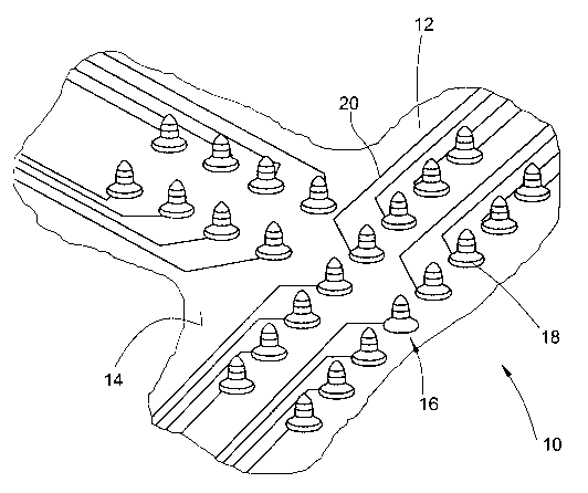
Figure 1 shows a device 10 according to the invention and represents a view
onto a circuit substrate 12 which can be a solid printed circuit board or a
flexible circuitry. On one of the major surfaces 14 of the substrate 12 an
array of e.g. 8x8 electrodes 16 and electrode contact pads 18 of the
substrate 12 can be identified, each of them being connected with its own
conductive trace 20. It is to be noted that an array of 8x8 electrodes is just
a specific example and that it is advantageous and desirable to increase the
number of electrodes to, for example, 16x16 corresponding to 256
individual electrodes. Even a higher number could be used. This is possible
and also realistic in view of the low manufacturing cost when using the
' technology as suggested in the invention. The electrodes 16 as such are
provided as so-called ball bumps as described hereinbelow and used in the
micro-electronic industry for connecting chips using the flip chip technology.
In Figure 2 a perspective view of a part of the electrode array on a larger
scale is shown. Each conductive trace 20 leads to a first contact pad 22 (see
Figure 1) which by some connection means is connectable to an electronic
device for generating and evaluating electrical signals to be applied to or
sensed by the individual electrodes 16. These electrical signals can
represent irripedances, currents, voltages, potentials, AC or DC or impulse
signals. The connection means can comprise a ball grid array (BGA), a. land
grid array (LGA) or contact pins and the like.
Figures 3 and 4 show in more detail the design and construction of a ball
bump electrode 16. This electrode 16 comprises a thickened socket portion
24 having a base end 26 for electrically and mechanically connecting the
socket portion 24 to an electrode contact pad 18. The shape of the socket
portion 24 looks like a flattened ball having a rounded periphery 28, wherein
CA 02426330 2003-04-22
WO 02/36002 PCT/EP00/10775
- 15 -
the lower side 30 of the socket portion 24 being flat so as to contact the
second contact pad 18. In the middle from the upper side 32 of the socket
portion 24 there protrudes a pointed portion 34 having a pointed end 36.
This pointed portion 34 contacts the surface (human or animal skin or organ
or tissue or cell) to be measured or investigated.
It is to be noted that Figures 3 and 4 schematically show the ball bump
which as of yet is used in the flip chip technology for connecting chips to a
circuitry layer with the structured side' of the chip facing the circuitry
layer.
In particular the pointed portion 34 can be longer and more needle-like or
sharper or both than depicted. The related technology for generating such
bumps and the typical use is described in a number of articles, for example
"Flip Chip Attachment Using Mechanical Bumps" by 3. Eldring et al., 1994,
ITAP & Flip Chip Proceedings, pages 74-81, "Flip Chip Attachment Using
Non-Conductive Adhesives and Gold Ball Bumps" by R. Aschenbrenner et al.
from the Technische Universitat Berlin, Forschungsschwerpunkt
Technologien der Mikroperipherik, TIB 4/2-1, or "Single Chip Bumping" by
Matthias Klein et al., Technical University of Berlin, Center of
Microperipheric
Technologies. The latter article describes the typical technology in more
detail. Thin wires of Au98Pd for example, with diameters between 18 and 33
micrometers are grabbed by a wire clamp and pressed on the contact area
to be connected. These contact areas can either be located on the flip chip
or the component, comprising the conductive paths such as a PCB. This can
be done utilizing a conventional ball-wedge bumping process, namely a wire
bonder, for example available from F&K Delvotech Bondtechnik GmbH,
Germany. The wire is passed through a capillary tube which forms the wire
clamp and an electrical discharge is applied which forms a ball establishing
the electrical and mechanical connection to the contact area to be
connected. This is identical to the well known wire bonding technique. In a
second step, however, the wire is torn off whereby it is ensured that this
rupture occurs within the heat effective zone where the grain structure of
the wire is coarser compared to the non-affected state. The rupture causes
CA 02426330 2003-04-22
WO 02/36002 PCT/EP00/10775
- 16 -
a lengthening of the wire with a significant simultaneous reduction of its
diameter until it becomes so thin that it ruptures. In this way a pointed
configuration is obtained which actually, for the intended purpose of the
electrical connection is undesirable.
The effect of such a process can be seen from Figure 3 which shows a
perspective view of such a mechanically applied gold stud bump on an
aluminium pad. Figure 4 shows a cross-sectional view showing the typical
dimensions. The overall diameter D of the ball bump ranges between 40 and
105 microns. The actual con-tact area B (base end 26) on the contact pad
18 to be contacted is typically 80 percent of the dimension D. The height h
of the socket portion 24 as shown in Figure 4 typically ranges between 12
and 65 microns. The height H is about 10 microns larger. The overall height
h' of the ball bump typically corresponds to the diameter D of the entire ball
bump. In this application heights of 100-200 microns are advantageous for
an optimum penetration of the pointed portion 34 and the pointed end 36
into the skin. Namely, the outermost portion of the skin typically has . a
thickness of around 100 microns which should be penetrated to establish a
good electrical contact. The actual pointed end 36 occurs in the upper part,
namely in that part of the overall height h' that exceeds H. The dimension b
is around half to 1/3 of the height h of the socket portion 24. The above
mentioned article refers to specific details of the ball bump in flip chip
technology application. For example it has been shown that the connection
to the contact pad 18 is sufFciently stable. Shear values in the area of 43-
60 cN/bump have been observed. Alternative alloys are PbSn2, PbSn6l; and
SnAg3 and relatively pure gold itself.
Figure 5 shows another embodiment of the device according to the
invention. This embodiment is rather similar to that of Figures 1 and 2. The
difference between these embodiments can be seen in the fact that in the
embodiment of Figure 5 the conductive traces 20 extend through the
substrate 12 in the thickness direction thereof with the end surfaces of the
CA 02426330 2003-04-22
WO 02/36002 PCT/EP00/10775
- 17 -
conductive traces 20 laying in the first and second major surfaces 14 of the
substrate 12 forming the second contact pads 18 and the first contact pads
22.
Figure 6 shows an alternative embodiment having is a configuration that in
principle is similar to the one depicted in Figures 1 and 2, however,
arranged in a non-flat configuration. Also here ball bump electrodes 16 have
been applied to contact pads of the flexible substrate 12. The substrate 12
is supported by a metal 38 stiffener which is arranged so that the
conductive traces 20 cannot be irritated as they are on the side 14 of the
substrate 12 facing away from the metal stiffener 38. The contact area with
the contact pads 22 can be a zebra strip, a ball grid array (BGA), or a land
grid array (LGA) 40.
Figure 7 shows an embodiment which is very similar to the one shown in
Figure 6 with the essential difference that instead of providing a metal plate
as a stiffener a plastic body 42 is applied which is solid in itself the whole
system, however, being essentially identical to the one shown in Figure 6.
Figure 8 shows an alternative embodiment in which the component with the
ball bump electrodes 16 is configured in a way to be discardable. The ball
bump electrodes 16 are applied to a flexible circuit layer substrate 12 having
BGA or LGA contact areas 44. The substrate 12 is fixed onto a plastic or
metal support part 46. The discardable component 48 can be attached to a
hand-held device 50. Accordingly this device 50 has to comprise mechanical
features like snapping means and the like (not shown) which allow to fix the
discardable component 48 onto the hand-held device 50 keeping it in a
position stable enough for the intended evaluation such as the generation of
an electrical or impedance image of a skin portion of a patient. The hand-
held device 50 includes the handle 52 as such which can be of a pistol type.
Furthermore, it includes a cable 54 connected to the connecting means 56
of the hand-held device 50 for connection to the BGA or LGA contact areas
CA 02426330 2003-04-22
WO 02/36002 PCT/EP00/10775
18 _
44 of the discardable component 48. At its other end (not shown) the cable
54 is connected or connectable to an evaluation unit, typically a computer
and a display unit.