Note: Descriptions are shown in the official language in which they were submitted.
CA 02426548 2003-04-16
WO 02/43456 PCT/USO1/43624
INTERFERENCE MITIGATION THROUGH CONDUCTIVE
THERMOPLASTIC COMPOSITE MATERIALS
TECHNICAL FIELD AND INDUSTRIAL
APPLICABILITY OF THE INVENTION
The present invention relates generally to electromagnetic radiation
interference
mitigation and, more particularly, to conductive thermoplastic composite
materials that
provide such interference mitigation by means of capacitive andlor inductive
electrical
coupling.
BACKGROUND OF THE INVENTION
In today's electronic age and particularly as a result of advances in digital
technologies, electrical malfunctions resulting from electromagnetic radiation
such as
radio frequency interference (RFI) have been proliferating. Recently, ever-
increasing
numbers of cordless and cellular phone users have compounded the problem. As a
result,
interference with clear communication and the shielding of communication
equipment
from stray radio frequency signals has become a primary concern.
As a result, many efforts have been made in recent years to mitigate RFI.
Examples of these efforts are found in U.S. Patents 5,371,404 to Juskey et al.
and 5,338,
617 to Workinger et al. The Juskey et al. patent discloses a semiconductor
device package
incorporating a thermally and electrically conductive plastic material
containing metal
particles that is transfer molded to encapsulate the semiconductor device. The
conductive
plastic material is electrically connected to the circuit ground to shield the
semiconductor
device from radio frequency energy and is mechanically attached to the
semiconductor
device to dissipate heat. Fins may be molded into the plastic conductive
material for heat
dissipation. The Worl~inger et al. patent discloses a radio frequency shield
that underlies
the conductors of a radio frequency assembly but does not enclose them. The
shield is
formed from metal powder particles in a plastic resin.
While the shields disclosed in the Juskey et al. and Workinger et al. patents
are
3o useful for their intended purpose, they are not without their shortcomings.
Specifically,
the Juskey et al. device package requires transfer molding so that the
semiconductor device
is encapsulated in the thermally and electrically conductive plastic material.
This transfer
molding requires the application of heat to the semiconductor device. This
limits the
CA 02426548 2003-04-16
WO 02/43456 PCT/USO1/43624
selection of shielding materials to relatively low temperature thermoplastic
materials since
higher temperature thermoplastic materials risk potential damage to the
semiconductor
device through the application of high temperatures. The Workinger et al.
shield does not
enclose the conductors or component to be shielded and as such fails to
provide sufficient
shielding for many applications.
Thus, a need is identified for an improved means of mitigating electromagnetic
radiation including radio frequency interference overcoming the above-
identified
disadvantages and limitations of the prior art.
SUMMARY OF THE INVENTION
In accordance with the purposes of the present invention as described herein,
an
electromagnetic radiation interference mitigation shield for an electronic
circuit
component is provided. That shield includes a body formed from an electrically
and
thermally conductive composite material characterized by a volume resistivity
ranging
from about 0.1 to about 1,000 ohm-cm and a thermal conductivity ranging from
about 10 x
10-4-cal.-cm./sec.-cm.2-°C to about 30 x 10-4-cal.-cm./sec.-cm.2-
°C.
The composite material of the body includes a plastic/polymer selected from a
group consisting of acrylonitrile butadiene styrene (ABS), polycarbonate (PC),
PC/ABS,
polypropylene (PP), nylon (PA), styrene acrylonitrile (SAN), polysulfone
(PSU),
polybutylene terephthalate (PBT), polyethylene terephthalate (PET),
polyphenylene
sulfide (PPS), polyimides (PI), polyester thermoplastic elastomer (TPE),
acrylic (PMMA),
rigid thermoplastic polyurethane (RTPU), liquid crystal polymer (LCP),
phenolics,
polyvinyl chloride (PVC), styrenics, cured polyester and epoxy resins, rubber,
silicone
RTV, and other elastomers, or any other similar thermoplastic, thermoset, or
room
temperature curing plastics or mixtures thereof.
Additionally, the body includes conductive particles selected from a group
consisting of conductive doping chemicals, metal-coated/plated
carbon/glass/plastic fibers,
metal-coated/plated carbon/glass/plastic particles, conductive metal fibers,
conductive
metal particles, metallic salts and any mixtures thereof. The conductive
particles are
provided in concentrations ranging from about 5% to about 50% by weight of the
composite material.
Metals utilized to coat or plate the carbon, glass or plastic fibers or
utilized
themselves as particles in the composite material are selected from a group
consisting of
2
CA 02426548 2003-04-16
WO 02/43456 PCT/USO1/43624
nickel, copper, iron, silver, gold, tin, zinc, lead, aluminum, brass, bronze,
stainless steel,
any mixtures thereof, and any other electrically conductive metals) not listed
herein.
Typically, the body of the shield includes a cavity for receiving the
electronic
circuit component to be shielded. Walls of the body defining the cavity are
adjacent to but
not physically touching the electronic circuit component. In most applications
the walls
are within 0.5 inches (1.27 centimeters) or less of the electronic circuit
component when
the shield is in the operative position relative to the electronic circuit
component to be
shielded.
In accordance with another aspect of the present invention, the electronic
radiation
l0 interference mitigation shield for an electronic circuit component may be
described as a
body of electrically and thermally conductive composite material formed from a
plastic
and conductive particles where the body has walls defining a cavity for
receiving the
electronic circuit component and the walls are within about 0.5 inches (1.27
centimeters)
or less of the electronic circuit component but not touching the electronic
circuit
component.
Still further, the invention may be described as an electronic radiation
interference
mitigation shield for an electronic circuit component comprising a body of
electrically and
thermally conductive composite material formed from a plastic selected from
but not
limited to a group consisting of acrylonitrile butadiene styrene,
polycarbonate, propylene,
nylon, styrene acrylonitrile, polysulfone, polybutylene terephthalate,
polyethylene
terephthalate, polyphenylene sulfide, polyimides, polyester thermoplastic
elastomer,
acrylic, polyvinyl chloride, styrenics, cured polyester and epoxy resins,
rubber, silicone
RTV and any mixtures thereof and conductive particles selected from a group
consisting
of conductive doping chemicals, metal-coated/plated carbon/glass/plastic
fibers, metal-
coated carbon/glass/plastic particles, conductive metal fibers, conductive
metal particles,
metallic salts and any mixtures thereof wherein the conductive particles are
provided at
concentrations ranging from about 5% to about 50% by weight of the composite
material.
In accordance with yet another aspect of the present invention a method of
shielding an electronic circuit component is provided. The method comprises
the step of
positioning over the electronic circuit component a separate body of
electrically and
thermally conductive composite material formed from a plastic and conductive
particles so
that walls of the body forming a cavity therein are positioned within about
0.5 inches (1.27
centimeters) of the electronic circuit component.
CA 02426548 2003-04-16
WO 02/43456 PCT/USO1/43624
BRIEF DESCRIPTION OF THE DRAWING
The accompanying drawing incorporated in and forming a part of the
specification,
illustrates several aspects of the present invention, and together with the
description serves
to explain the principles of the invention.
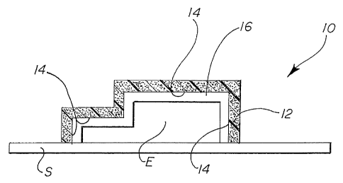
The Fig. is a partially schematical, cross-sectional view of the present
invention
showing the electromagnetic radiation interference mitigation shield
positioned on a
circuit board substrate over an electronic circuit component to be shielded.
Reference will now be made in detail to the present preferred embodiment of
the
1o invention, an example of which is illustrated in the accompanying drawing.
DETAILED DESCRIPTION OF THE INVENTION
Reference is now made to The Fig. showing the electromagnetic radiation
interference mitigation shield 10 of the present invention for shielding an
electronic circuit
15 component such as shown at E mounted to a circuit board substrate S.
The shield 10 comprises a body 12 having a series of walls 14 that define a
cavity
16 substantially conforming to the shape of the electronic circuit component E
to be
shielded. Specifically, the shield 10 is positioned over the electronic
circuit component E
so that the walls 14 defining the cavity 16 are within 0.5 inches (1.27
centimeters) or less
20 of the exterior of the electronic circuit component E being shielded. The
body 12 of the
shield 10 is then anchored in position on the substrate S by adhesive,
fasteners or any other
appropriate means known in the art.
The body 12 of the shield 10 is formed from an electrically and thermally
conductive composite material. That material is characterized by a volume
resistivity
25 ranging from about 0.1 to about 1,000 ohm-cm and a thermal conductivity
ranging from
about 10 x 10-~-cal.-cm./sec.-cm.2-°C to about 30 x 10~'-cal.-cm./sec.-
cm.z-°C.
The body 12 includes a plastic/polyrner selected from a group consisting of
acrylonitrile butadiene styrene (ABS), polycarbonate (PC), PC/ABS,
polypropylene (PP),
nylon (PA), styrene acrylonitrile (SAN), polysulfone (PST, polybutylene
terephthalate
30 (PBT), polyethylene terephthalate (PET), polyphenylene sulfide (PPS),
polyimides (PI),
polyester thermoplastic elastomer (TPE), acrylic (PMMA), rigid thermoplastic
polyurethane (RTPT~, liquid crystal polymer (LCP), phenolics, polyvinyl
chloride (PVC),
styrenics, cured polyester and epoxy resins, rubber, silicone RTV, and other
elastomers
4
CA 02426548 2003-04-16
WO 02/43456 PCT/USO1/43624
and any mixtures thereof.
The body also includes conductive particles selected from a group consisting
of
conductive doping chemicals (for example, iron compounds, arsenic compounds,
allcali
metals), metal-coated/plated carbon/glass/plastic fibers (for example, nickel,
silver, copper
plated), metal-coated carbon/glass/plastic particles (for example, nickel,
silver, copper
plated), conductive metal fibers, conductive metal particles, metallic salts
(for example,
ferric, diazonium) and any mixtures thereof. The metals used as fibers or to
coat or plate
carbon, glass or plastic include nickel, copper, iron, silver, gold, tin,
zinc, lead, aluminum,
brass, bronze, stainless steel, and any mixtures thereof. Of course, while not
specifically
listed other electrically conductive metals including various alloys could be
utilized. The
conductive particles are provided in the body 12 of the shield 10 in
concentrations ranging
from about 5% to about 50% by weight of the composite material.
It should be appreciated that the shield 10 may be easily molded to any
desired
shape for any particular application. Accordingly, the present invention
provides
application specific or designed shielding customized to any particular
application. This
allows increased electromagnetic/radio frequency interference shielding of
specific
circuitry "hot spots". By this, it is meant that the RFI and EMI shielding may
be
concentrated at the electronics that are the source of the radiation where
that radiation may
be most easily isolated and contained. As the shield 10 is custom molded to
the required
2o shape for the sluelding application, shielding materials are minimized.
Further, since a
composite material is utilized for the body 12 of the shield 10, undesirable
energy
reflections typical of metal and metal plated plastic RF shields are avoided.
This is
because the shield accomplishes the removal of undesirable EM or RF energy by
effecting
an inductive and/or capacitive coupling of the walls 14 of the body 12 to the
radiating RF
signal, thereby causing the energy to be absorbed into the conductive plastic
and
conducted into adjoining areas of the main electronics housing (for example,
the substrate
S). This produces a heating effect proportional to the level of energy
absorbed. The heat
is then gradually dissipated from the shield via radiation to the surrounding
environment.
In order to be most effective, the walls 14 of the shield 10 are positioned in
close
3o proximity to the electronic circuit component E to be shielded. The maximum
distance
between the walls 14 and the component E is about 0.5 inches (1.27
centimeters) or less.
For best results, the shield 10 is not, however, positioned in direct contact
or touching the
electronic circuit component E as direct thermal heating of the shield from
the electronic
CA 02426548 2003-04-16
WO 02/43456 PCT/USO1/43624
component E being shielded could adversely affect the energy absorbing and
heat
dissipating properties of the shield.
It should be appreciated that as a result of the shield 10 shielding through
absorption rather than reflection, RF energy gasketing is not necessary to
prevent gap or
slot leakage of RF radiation to surrounding environments. Thus, this
additional expense
characteristic of metal and metal plated plastic shields is avoided. Further,
since the shield
is separate from and not encapsulated around the electronic component E it
should be
appreciated that the electronic component E is not subjected to high
temperatures during
transform molding that would otherwise be necessary to complete encapsulation.
Further,
1o the shield 10 may be removed if desired to access the underlying electronic
circuit
component for maintenance or any other purpose.
The foregoing description of a preferred embodiment of this invention has been
presented for purposes of illustration and description. It is not intended to
be exhaustive or
to limit the invention to the precise form disclosed. Obvious modifications or
variations
are possible in light of the above teachings. The embodiment was chosen and
described to
provide the best illustration of the principles of the invention and its
practical application
to thereby enable one of ordinary skill in the art to utilize the invention in
various
embodiments and with various modifications as are suited to the particular use
contemplated. All such modifications and variations are within the scope of
the invention
2o as determined by the appended claims when interpreted in accordance with
the breadth to
which they are fairly, legally and equitably entitled.
6