Note: Descriptions are shown in the official language in which they were submitted.
CA 02426651 2003-04-28
METHOD AND APPARATUS FOR TRANSFERRING
SOLDER BUMPS
Field of the Invention
This invention relates to electronic packages, methods and apparatus
pertaining to
manufacturing aspects thereof and in particular, electronic packages wherein
electrical
interconnections are achieved by solder bumps such as for mounting an
integrated
circuit device on a substrate.
Background of the Invention
In present day manufacturing of electronic packages, microcircuits such as
integrated
circuits or semiconductor chips are frequently attached to other chips or
other electronic
circuit carrying structures. The attachment of a chip device is frequently
accomplished
by one of two techniques. The first technique is the use of wire bonding
whereby each
of the series of I/O bump terminals on a chip is sequentially bonded to
corresponding
connecting pads on a substrate. The second technique is a flip chip attachment
in
which all the I/O bumps on a chip are first terminated with a solder material.
The chip is
then flipped over and the solder bumps are aligned and reflowed in a reflow
furnace to
effect all of the I/O connections with bonding pads on the substrate. An
advantage
achieved by the flip chip process is its applicability to very high density
circuits and its
reliability in the interconnections formed when compared to wire bonding
processes.
There are a variety of ways that are presently used in the formation of solder
bumps on
a chip or substrate. Often, the formation of solder balls is carried out by a
method of
evaporating lead and tin mixtures through a mask for producing the desired
solder
bumps. Techniques of electrodeposition of such mixtures have also been used to
produce solder balls in flip chip packaging.
CA9-2002-0078 1
CA 02426651 2003-04-28
Another popular technique is the use of a process of solder paste screening.
However,
with the recent trends in miniaturization of integrated circuits and device
dimensions
and the reduction of pitch or the spacing between bumps, the solder paste
screening
technique becomes less practical. In the solder paste screening process, since
the
solder paste is normally applied directly to the substrates through a screen
mask which
contains holes aligned to the paste receiving pads on the substrate, any
problems
occurring during the process may result in the requirement that the substrate
must be
reworked.
A more recently developed injection molded solder technique dispenses molten
solder
instead of solder paste. An advantage of this process results from very little
volume
change occurring between the molten solder and the resulting solder bump. This
process is typically practiced by first filling with solder a mold containing
holes or
cavities aligned to the pads on the substrate. Next, the filled mold is placed
in close
proximity to a substrate which contains solder receiving pads and onto which
flux
material has typically been dispensed in a thin layer over the substrate. When
the
solder in the mold is heated to a melting temperature in a furnace, surface
tension
reduction causes the solder to ball up and intimately contact the solder
receiving pad,
which is normally covered with gold or other solder wetting alloy. A wiper may
be used
after the molten solder fills the holes to remove excess solder. However, when
this
technique is used on large substrates, the balling up of the solder may be
insufficient to
ensure intimate contact between the solder in the mold cavities and solder
receiving
pads on the substrate and thus the solder balls may not adequately adhere to
the
contact pads.
One prior art technique for overcoming the difficulties of known processes in
forming
solder bumps for integrated circuit interconnections is described in U.S.
Patent No.
6,003,757 entitled Apparatus for Transferring Solder Bumps and Method of
Using,
issued December 21, 1999 and assigned to International Business Machines
Corporation. This patent describes a method and apparatus to maintain a solder
mold
in intimate contact with the solder receiving substrate, for example a
semiconductor
CA9-2002-0078 2
CA 02426651 2003-04-28
wafer, during a solder reflow operation such that the solder in the mold is
transferred to
solder wettable pads on the receiving substrate. A uniform pressure on the
mold
substrate assembly is necessary to ensure that all solder segments from the
mold
cavities are able to contact all solder wettable pads on the substrate at the
time that the
solder becomes molten. As described in U.S. Patent 6,003,757, the apparatus
applies
such a uniform pressure until physical disassembly by human intervention as by
opening the lid of the clamshell assembly of the apparatus releases the
pressure. Such
human intervention must occur after the mold-substrate assembly has exited the
reflow
furnace and cooled. Due to the pressure, the molten solder has maintained the
shape
of the mold cavity in which it was located and in effect, is somewhat adhering
to most or
all of the mold cavity surfaces. Although this is not a metallurgical bond in
the sense of
the solder-substrate pad intertace which is a strong metallurgical bond,
separating the
mold from the cavity nonetheless requires a certain tensile force and care
must be
taken to avoid any shearing motion. Both of these latter conditions risk
unintended
separation of the metallurgical bond between the solder and substrate pad. To
reduce
such risk, the mold-substrate assembly is subjected to a second solder reflow
operation
after the uniform pressure has been physically released. At this stage without
any
compressive forces present and with gravitational forces minimized by
orienting the
assembly such that the lighter substrate is on top, the remelted solder, now
metallurgically bonded to the substrate pad, will tend to partially ball up,
thus forcing the
mold and the substrate to partially separate and facilitate physical
separation of the two.
Once successfully separated, it is often desired to have perfectly rounded
solder bumps
on the substrate in order to optimize subsequent assembly operations. This
thus
suggests yet another solder reflow operation of the substrate alone.
The shortcomings of the prior art and in particular the arrangements as
described in
U.S. Patent No. 6,003,757, are addressed by the aspects of the present
invention. The
apparatus and method of this invention provides for the removal of intimate
contact
between the mold and the substrate at a prescribed point in the process during
the
reflow operation. By doing so, the transfer of solder from a mold to solder
wettable
substrate pads of a substrate, the separation of mold from the substrate and
the
CA9-2002-0078 3
CA 02426651 2003-04-28
uniform balling shape of the transferred solder bumps on the substrate, can be
accomplished by a single solder reflow process instead of two or three as may
be
required in the prior art.
Summaryr of the Invention
The present invention relates to eliminating the difficulties in forming
uniform solder
bails, for example, for the attachment of integrated circuit devices on
substrates as well
as other shortcomings resulting from existing technology. The present
invention has
the object to provide techniques which alleviate the above described and other
drawbacks.
According to one aspect of the present invention, there is provided a method
of
transferring solder bumps from a mold to a substrate having a plurality of
pads by
providing a base member and a substrate located thereon and positioning a mold
having a plurality of solder elements on said substrate such that each solder
element
contacts a corresponding pad on the substrate and the mold contacts at least
one
compressible device located on the base member. The mold is caused to compress
the compressible device and the solder elements are heated such that each
solder
element melts and transfers to a corresponding pad. The compressible device is
caused to decompress to thereby separate the substrate and the mold while the
solder elements are melted whereby each solder element remains on its
corresponding
pad in the form of a solder bump and the solder bumps are solidified.
According to another aspect of the present invention there is provided
apparatus for
transferring solder bumps from a mold to a substrate having a plurality of
pads where
the apparatus has a base member and a substrate located thereon. A mold having
a
plurality of solder elements is positioned on the substrate such that each
solder
element contacts a corresponding pad on the substrate and the mold contacts a
compressible device located on the base member. Means causes the mold to
compress the compressible device. Reflow means melts the solder elements and
CA9-2002-0078 4
CA 02426651 2003-04-28
causes each of the solder elements to transfer to a corresponding pad. Means
decompresses the compressible device causing the substrate and mold to
separate
while the solder elements are melted resulting in each said solder element
remaining
on its corresponding pad in the form of a solder bump.
Brief Description of the Drawinc,~s
The above and other advantages of the present invention will be better
understood with
reference to the following drawings wherein like reference numbers represent
like
elements of the invention embodiments:
Figure 1 is an isometric drawing of a perspective representative of a transfer
fixture
apparatus for mounting and holding a wafer or similar object to which solder
bumps are
transferred in accordance with a preferred embodiment of aspects of the
present
invention;
Figure 2 is a cross-sectional view of the apparatus shown in Figure 1 as
indicated by
the arrows A-A, showing more details of the compressible devices of the
transfer
fixture apparatus and the mechanisms to compress and decompress the
compressible
devices, according to a preferred embodiment of the present invention;
Figure 3 is an illustrative drawing showing in greater detail the positioning
of the
elements of a preferred embodiment of the invention prior to heat being
applied to melt
the solder slug of the transfer fixture apparatus;
Figure 4 is similar to Figure 3 wherein the temperature has been raised to
cause the
solder slug to melt; and
Figure 5 is similar to Figures 3 and 4 wherein the mold has been separated
from the
substrate.
CA9-2002-0078 5
CA 02426651 2003-04-28
Detailed Description of the Preferred Embodiments
The preferred embodiments of the present invention discloses methods and
apparatus
which provide for opposing forces to occur within a transfer assembly to
thereby
enhance the transfer of solder bumps from a mold to a substrate. A backing
plate and
lid member of the transfer fixture, continue to provide a compressive force to
a mold
and substrate assembly while a base member is provided with compressible
devices
forced against the mold outside of the interface area between the mold and
substrate.
While the compressive forces imparted by the backing plate and lid member
exceed the
decompressing forces of the compressible devices, the mold and substrate
remain in
contact with each other. As soon as the compressive forces resulting from the
backing
plate and lid member are eliminated or sufficiently reduced, the decompression
of the
compressible devices results in the mold moving upwards and away from the
substrate.
In order to achieve the advantages of the subject invention, in a preferred
embodiment,
a heat physically changeable device is provided to eliminate or sufficiently
reduce the
forces applied to the lid member and backing plate while the mold and
substrate
assembly and transfer mechanism are still in a reflow furnace and the solder
bumps to
be transferred are still in their molten states.
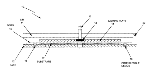
Figure 1 is a perspective view of a transfer fixture or mechanism 10 for
implementing a
preferred embodiment of the present invention. Fixture 10 comprises a lid 11
appropriately movably attached to base member 12. Such attachment could, for
example, be hinge 20. Lid 11 can be of any appropriate design and shape and as
shown in Figure 1, lid 11 in the shape of the letter "H" would be suitable.
Centrally
located in fixture 10 and operatively attached to lid 11 is a compressing pin
15, the
function of which will be further described with reference to Figure 2. Mold
13 overlays
a substrate or wafer to which solder bumps are to be formed, transferred and
attached
to wettable receiving pads on the substrate. The wafer or substrate is not
readily
shown in Figure 1 but will be apparent and further described with reference to
subsequent drawing figures. Backing plate 14 is configured to uniformly exert
pressure
on mold 13. Any appropriate design of backing plate 14 may be employed as long
as
CA9-2002-0078 6
CA 02426651 2003-04-28
substantially uniform pressure is applied to mold 13. The pressure is
initiated by forces
resulting from compressing pin 15 which applies pressure to backing plate 14
through a
device which can have its shape physically changed by the application of heat.
In the
preferred embodiment of the invention, the heat physically changeable device
can be a
S slug of solid solder as will be subsequently more fully described.
With reference to Figure 2, which is a cross-sectional view of the preferred
transfer
fixture of Figure 1 as shown by the arrows A-A, substrate 17 is shown located
on base
member 12 over which is located mold 13. Mold 13 is shown abutting against
compressible devices 18. Compressible device 18 consists of one or more
devices
suitably positioned at locations in fixture 10 between mold 13 and base 12.
Compressible device or devices 18 could be in the form of springs. When mold
13 is
forced against substrate 17, the compressible device 18 is caused to become
compressed. At this point compressible device 18 is in a compressed state.
Mold 13
has a plurality of cavities in which solder elements have been placed and
these solder
elements in turn contact pads on the surface of substrate 17, which will be
subsequently illustrated and more fully described. Thus in fixture 10 as shown
in the
drawing of Figure 2, when lid 11 is in its closed position on base 12 as
shown,
compressing pin 15 is forced against solder slug 16 which in turn causes
pressure to be
applied to backing plate 14 and mold 13, thereby compressing compressible
devices
18.
Compressing pin 15 would typically be a spring-loaded pin. An interference fit
is
designed between pin 15 and lid 11 and a force is transmitted from pin 15 to
subsequent elements below pin 15, namely solder slug 16, backing plate 14,
mold 13,
substrate 17 and base member 12, when lid 11 is fixed in its closed position
with
respect to base member 12. The interference fit will cause spring-loaded pin
15 to
compress thereby exerting a force against slug 16 and in turn against backing
plate 14
and in turn against mold 13 which causes compressible devices 18 between mold
13
and base 12 to compress.
CA9-2002-0078 7
CA 02426651 2003-04-28
Compressing pin 15 and compressible devices 18 are designed to provide
appropriate
compressive forces. Material selection of backing plate 14 is such that it is
non-wettable to the solder of solder slug 16. Fixture 10 also has appropriate
means
(not shown), vacuum or otherwise, to hold substrate 17 against base 12 such
that,
during separation of mold 13 from substrate 17, the surface tension forces of
the
molten solder between said mold 13 and said substrate 17 are overcome and
substrate
17 remains on base 12.
In summary with reference to Figures 1 and 2, lid 11 contains compressing pin
15
which abuts against backing plate 14 by means of a slug of solid solder 16
between pin
and backing plate 14. Backing plate 14 in turn abuts against the top side of
the
assembly of mold 13 and substrate 17. Heat deformable solid solder element or
slug
16 is of material of a higher melting point than the solder elements used in
cavities of
mold 13 to be transferred as solder bumps to substrate 17 yet of a lower
melting point
15 than the peak temperature that is achieved in the reflow temperature
profile as
appropriately selected for the solder elements in mold 13. Thus, solder slug
16 will only
melt after the solder elements in mold 13 to be transferred have melted and
wetted the
solder wettable pads of substrate 17. When solder slug 16 does melt, it can no
longer
act as a solid interface between compressing pin 15 and backing plate 14 and
hence
backing plate 14 no longer exerts a significant compressive force against the
assembly
of mold 13 and substrate 17. At this point, compressive device or devices 18
located
between base member 12 and mold 13 will force mold 13 upwards, thus separating
mold 13 from substrate 17. Substrate 17 however has been held in place on base
member 12 for a sufficient length of in time whereby the transferred solder
balls have
wetted the pads on substrate 17 and are still molten. When the cavities of
mold 13 no
longer restrict the shape of the transferred solder bumps, the solder bumps
are free to
revert to their lowest energy shape which is as spherical as possible a shape,
as
determined by the existence of metallurgical bonds between each one of the
solder
bumps and a solder wettable pad on substrate 17 upon which the solder bump is
located.
CA9-2002-0078 8
CA 02426651 2003-04-28
Examples of selections for the solder alloy constituting solder slug 16 will
now be
described. If the solder bumps to be transferred to substrate 17 are made of
eutectic
tin/lead (63% Sn, 37% Pb) with a melting point of 183 degrees C, typical
solder reflow
profiles may have a maximum peak temperature of 215 to 230 degrees C. For the
purpose of this example, let us say the average peak temperature is 225
degrees C.
One possible alloy for solder slug 16 is Sn3.5Ag0.7Cu (hereinafter referred to
as SAC)
which melts at 217 degrees C. When the solder reflow temperature profile
reaches 183
degrees C, the solder bumps will start to melt and wet the corresponding pads
on
substrate 17. Some time later, when the solder reflow temperature profile
reaches 217
l0 degrees, the SAC solder slug 16 will melt. This releases or decreases the
compressive
forces between pin 15 and backing plate 14 and thus mold 13. Compressible
devices
18 between base member 12 and mold 13 will now be able to force mold 13
upwards
and away from substrate 17 which is being held on base 12. As mold 13 moves
away
from substrate 17, backing plate 14 is similarly caused to move upwards,
forcing the
liquid SAC solder 16 to flow around the compressive pin 15. This continues as
the
solder reflow temperature profile of the solder bumps rises to a 225 degree C.
peak and
then descends back to 217 degrees C. At 217 degrees C, the SAC solder 16
solidifies
in its position around compressive pin 15 with backing plate 14 and mold 13
still in their
upward position as forced there by the compressible devices 18 on base member
12.
The eutectic solder of the solder bumps is still molten at 217 degrees C and
is no
longer restricted in shape by the cavities of mold 13 but are attached to the
pads of
substrate 17 and will tend to ball up into a rounded shape because of their
adherence
to respective pads on the substrate and will subsequently solidify in this
shape as the
temperature profile descends below 183 degrees C.
The various phenomena and activities that have been described above with
respect to
the transfer of solder bumps from mold 13 to substrate 17 will now be further
described
and illustrated with reference to the various diagrams, Figures 3, 4 and 5,
illustrating
various stages of the formation of the solder bumps. As shown in Figures 3, 4
and 5,
the transfer mechanism or fixture 10 as previously described with reference to
Figure 1
is diagrammatically shown. Wafer, or substrate, 17 is illustrated as being
mounted on
CA9-2002-0078 9
CA 02426651 2003-04-28
foam 34 on base 12. Foam 34 is optional in achieving the beneficial results of
the
invention, but it is found to be useful to result in a more uniform pressure
being applied
between mold 13 and wafer or substrate 17. In any event, as previously
described,
substrate 17 is appropriately held against base 12. Mold 13 has a plurality of
cavities
30 in which are located solder elements 31. Substrate 17 has a plurality of
solder
wettable pads 32 which coincide with and are aligned with each of the cavities
30 of
mold 13. Figure 3 shows the initial position of the various elements of
apparatus 10
once lid 11 has been appropriately attached to fixture frame 33 and
compressing pin
applies pressure to backing plate 14 through solder slug 16 as has been
previously
10 described. At a temperature range up to 183 degrees C., at which solder
elements 31
begin to melt, solder elements 31 in mold cavities 30 have not yet wet pads 32
on
wafer 17. As the temperature profile increases however, and solder elements 31
begin
to melt and as the temperature rises from 183 degrees C to 217 degrees C, the
arrangement as shown in Figure 3 continues to exist, however solder elements
or
15 bumps 31 in mold cavities 30, have melted and wet the respective pads 32 on
substrate
17
With reference to Figure 4, the diagrammatic representation of transfer
fixture 10 is
shown as the temperature rises above 217 degrees C, at which point solder slug
16
melts and is no longer a solid element below pin 15 but instead it surrounds
the
compressing pin 15 thereby reducing the compressive forces applied by lid 11
through
pin 15 on backing plate 14 and mold 13. This results in backing plate 14 and
mold 13
being pushed upward by compression springs 18. As can be seen, compression
springs 18 are elongated and decompressed in Figure 4 when compared with the
illustration in Figure 3.
With reference to Figure 5, the diagrammatic representation of fixture 10 is
shown with
the temperature being between 217 degrees C and 225 degrees C, solder bumps 31
are no longer restrained by cavities 30 in mold 13 but are wetted to pads 32
on
substrate 17 and are thus caused to ball up as shown and as previously
described.
CA9-2002-0078 10
CA 02426651 2003-04-28
Once fixture 10 is removed from the reflow furnace and the temperature profile
is
caused to descend below 183 degrees C, solder bumps 31 will solidify, remain
attached
to pads 32 on substrate 17 and thus remain in the spherical configuration as
shown in
Figure 5.
Other means and arrangements could be used to achieve similar intended results
of
eliminating and reducing the compressive forces applied by lid 11 in fixture
10 at the
appropriate point where solder elements 31 from mold 13 have transferred to
pads 32
on substrate 17 while they are still in a molten state. These alternative
embodiments
would be apparent to one of ordinary skill in this art. For example, a spring
mechanism
for imparting compressive forces on backing plate 14 resulting from
compressing pin 15
could be designed to diminish the applied forces at a prescribed time, where
the time is
correlated to the time dependent temperature profile of the reflow furnace.
Alternatively, the release or decrease of the applied force could be affected
at a
prescribed temperature by the use of a temperature sensor. Alternatively, the
spring
mechanism could be made of a material that has a temperature-dependent spring
constant such that at the desired temperature the spring constant is
sufficiently low that
the compressing pin 15 exerts little or no compressive force on backing plate
14 and
mold 13, permitting the compressible devices 18 to decompress and move mold 13
away from substrate 17 as has been described above.
It will be understood from the foregoing descriptions and illustrations that
various
modifications and changes may be made to the described and illustrated
preferred
embodiments of the present invention without departing from the true intent
and spirit of
the subject invention. It is intended that the above description is for the
purposes of
illustration only and should not be construed in a limiting sense. It should
be
appreciated that particular arrangements shown or described are provided
essentially
for convenience in presenting the invention and those of ordinary skill in the
art would
understand that the scope of the invention is not limited to the number,
sizes,
dimensions or arrangements of the various elements shown. The scope of the
invention should be limited only by the language of the claims which follow.
CA9-2002-0078 11