Note: Descriptions are shown in the official language in which they were submitted.
CA 02426718 2003-04-22
WO 02/37579 PCT/USO1/45636
GROUP III NITRIDE LIGHT EMITTING DEVICES WITH
GALLIUM-FREE LAYERS
FIELA OF THE INVENTION
The present invention relates to semiconductor
structures of light emitting devices, particularly light
emitting diodes and laser diodes formed from Group III
nitrides, which are capable of emitting light in the red
to ultraviolet portions of the electromagnetic spectrum.
BACKGROUND OF THE INVENTION
Photonic semiconductor devices fall into three
categories: devices that convert electrical energy into
optical radiation (e. g, light emitting diodes and laser
diodes); devices that detect optical signals (e. g.,
photodetectors); and devices that convert optical
radiation into electrical energy (e. g., photovoltaic
devices and solar cells). Although all three kinds of
devices have useful applications, the light emitting
diode may be the most commonly recognised because of its
application to various consumer products and
applications.
Light emitting devices (e. g., light emitting diodes
and laser diodes), herein referred to as LEDs, are
photonic, p-n junction semiconductor devices that convert
electrical power into emitted light. Perhaps most
commonly, LEDs form the light source in the visible
portion of the electromagnetic spectrum for various
signals, indicators, gauges, and displays used in many
consumer products (e. g., audio systems, automobiles,
household electronics, and computer systems). LEDs are
desirable as light output devices because of their
CA 02426718 2003-04-22
WO 02/37579 PCT/USO1/45636
-2-
generally long lifetime, their low power requirements,
and their high reliability.
Despite widespread use, LEDs are somewhat
functionally constrained, because the color that a given
LED can produce is limited by the nature of~the
semiconductor material used to fabricate the LED. As
well known to those of ordinary skill in this and related
arts, the light produced by an LED is referred to as
"electroluminescence," which represents the generation of
light by an electric current passing through a material
under an applied voltage. Any particular composition
that produces electroluminescent light tends to do so
over a relatively narrow range of wavelengths.
The wavelength of light (i.e., its color) that can
be emitted by a given LED material is limited by the
physical characteristics of that material, specifically
its bandgap energy. Bandgap energy is the amount of
energy that separates a lower-energy valence band and a
higher energy conduction band in a semiconductor. The
bands are energy states in which carriers (i.e.,
electrons or holes) can reside in accordance with well-
known principles of quantum mechanics. The "band gap" is
a range of energies between the conduction and valence
bands that are forbidden to the carriers (i.e., the
carriers cannot exist in these energy states). Under
certain circumstances, when electrons and holes cross the
bandgap and recombine, they will emit energy in the form
of light. In other~words, the frequency of
electromagnetic radiation (i.e., the color) that~can be
produced by a given semiconductor material is a function
of that material's bandgap energy.
CA 02426718 2003-04-22
WO 02/37579 PCT/USO1/45636
-3-
In this regard, narrower bandgaps produce lower
energy, longer wavelength photons. Conversely, wider
bandgap materials produce higher energy, shorter
wavelength photons. Blue light has a shorter wavelength-
s and thus a higher frequency-than the other colors in the
visible spectrum. Consequently, blue light must be
produced from transitions that are greater in energy than
those transitions that produce green, yellow, orange, or
red light. Producing photons that have wavelengths in
~ the blue or ultraviolet portions of the visible spectrum
requires semiconductor materials that have relatively
large bandgaps.
The entire visible spectrum runs from the violet at
or about 390 nanometers to the red at about 780
nanometers. In turn, the blue portion of the visible
spectrum can be considered to extend between the
wavelengths of about 425 and 480 nanometers. The
wavelengths of about 425 nanometers (near violet) and 480
nanometers (near green) in turn represent energy
transitions of about 2.9 eV and about 2.6 eV,
respectively. Accordingly, only a material with a
bandgap of at least about 2.6 eV can produce blue light.
Shorter wavelength devices offer a number of
advantages in addition to color. In particular, when
used in optical storage and memory devices, such as CD-
ROM optical disks, shorter wavelengths enable such
storage devices to hold significantly more information.
For example, an optical device storing information using
blue light can hold substantially more information in the
same space as one using red light.
CA 02426718 2003-04-22
WO 02/37579 PCT/USO1/45636
-4-
The basic mechanisms by which light-emitting diodes
operate are well understood in this art and are set
forth, for example, by Sze, Physics of Semiconductor
Devices, 2d Edition (1981) at pages 681-703.
The common assignee of the present patent
application was the first in this field to successfully
develop commercially viable LEDs that emitted light in
the blue color spectrum and that were available in large,
commercial quantities. These LEDs were formed in silicon
carbide, a wide-bandgap semiconductor material. Examples
of such blue LEDs are described in U.S. Patent Nos.
4,918,497 and 5,027,168 to Edmond each titled "Blue Light
Emitting Diode Formed in Silicon Carbide." Other
examples of Group III nitride LED structures and laser
structures are described in commonly assigned U.S.
Patents Nos. 5,523,589; 5,592,501; and 5,739,554.
In addition to silicon carbide, candidate materials
for blue light emitting~devices are gallium nitride (GaN)
and its associated Group III (i.e.; Group III of the
periodic table) nitride compounds such as aluminum
gallium nitride (AlGaN), indium gallium nitride (InGaN),
and in some circumstances aluminum indium gallium nitride
(AlInGaN). These materials are particularly attractive
because they offer direct energy transitions with
bandgaps between about 1.9 to about 6.2 eV at room
temperature. More common semiconductor materials such as
silicon, gallium phosphide, or gallium arsenide are
unsuitable for producing blue light because their
bandgaps are approximately 2.26 eV or less, and in the
case of silicon, are indirect semiconductors and
inefficient light emitters.
CA 02426718 2003-04-22
WO 02/37579 PCT/USO1/45636
-5-
As known to those familiar with LEDs and electronic
transitions, a direct transition occurs in a
semiconductor when the valence band maxima and the
conduction band minima have the same momentum state.
This means that crystal momentum is readily conserved
during recombination of electrons and holes so that the
energy produced by the transition can go predominantly
and efficiently into the photon, (i.e., to produce light
rather than heat). When the conduction band minimum and
valence band maximum do not have the same momentum state,
a phonon (i.e., a quantum of vibrational energy) is
required to conserve crystal momentum and the transition
is called "indirect." The necessity of a third particle,
the phonon, makes indirect radiative transitions less
likely, thereby reducing the light emitting efficiency of
the device.
Generally speaking, an LED formed in a direct
bandgap material will perform more efficiently than one
formed in an indirect bandgap material. Therefore, the
~ direct transition characteristics of Group III nitrides
offer the potential for brighter and more efficient
emissions-and thus brighter and more efficient LEDs-than
do the emissions from indirect materials such as silicon
carbide. Accordingly, much interest in the last decade
has also focused on producing light emitting diodes in
gallium nitride and related Group III nitrides.
Although Group III nitrides offer a direct
transition over a wide bandgap energy range, the material
presents a particular set of technical manufacturing
problems. In particular, no commercially-viable
technique has yet emerged for producing bulk single
CA 02426718 2003-04-22
WO 02/37579 PCT/USO1/45636
-6-
crystals of gallium nitride (GaN) that are capable of
functioning as appropriate substrates for the gallium
nitride epitaxial layers on which photonic devices would
be formed.
All semiconductor devices require some kind of
structural substrate. Typically, a substrate formed of
the same material as the active region offers significant
advantages, particularly in crystal growth and lattice
matching. Because gallium nitride has yet to be formed
in such bulk crystals, gallium nitride photonic devices
must be formed in epitaxial layers on non-GaN substrates.
Recent work in the field of Group III nitride
substrates includes copending and commonly assigned U.S.
patent applications Serial Nos. 09/361,945, filed July
27, 2999, for "Growth of Bulk Single Crystals of Aluminum
Nitride;" 09/361,944 filed July 27, 1999, for "Growth of
Bulk Single Crystals of Aluminum Nitride from a Melt;"
09/111,413 filed July 7, 1999, for "Growth of Bulk Single
Crystals of Aluminum Nitride;" and 09/169,385 filed
October 9, 1998, for "Growth of Bulk Single Crystals of
Aluminum Nitride: Silicon Carbide Alloys." All of these
pending applications are incorporated entirely herein by
reference. '
Using different substrates, however, causes an
additional set of problems, mostly in the area of crystal
lattice matching. In nearly all cases, different
materials have different crystal lattice parameters. As
a result, when a gallium nitride epitaxial layer is grown
on a different substrate, some crystal lattice
mismatching and thermal expansion coefficient mismatching
will occur. The resulting epitaxial layer is referred to
CA 02426718 2003-04-22
WO 02/37579 PCT/USO1/45636
as being "strained" by this mismatch. Crystal lattice
mismatches, and the strain they produce, introduce the
potential for crystal defects. This, in turn, affects
the electronic characteristics of the crystals and the
junctions, and thus tends to degrade the performance of
the photonic device. These kinds of defects are even
more problematic in high power structures.
In early Group III nitride LEDs, the most common
substrate for gallium nitride devices was sapphire (i.e.,
aluminum oxide A1~03). Certain contemporary Group III
nitride devices continue to use it.
Sapphire is optically transparent in the visible and
ultraviolet ranges, but has a crystal lattice mismatch
with gallium nitride of about 16 percent. Furthermore,
sapphire is insulating rather than conductive, and is
unsuitable for conductivity doping. Consequently, the
electric current that must be passed through an LED to
generate the light emission cannot be directed through a
sapphire substrate. Thus, other types of connections to
the LED must be made.
In general, LEDs with vertical geometry use
conductive substrates so that ohmic contacts can be
placed at opposite ends of the device. Such vertical
LEDs are preferred for a number of reasons, including
their easier manufacture and more simple incorporation
into end-use devices than non-vertical devices. In the
absence of a conductive substrate, however, vertical
devices cannot be formed.
In contrast with sapphire, gallium nitride only has
a lattice mismatch of about_2.4 percent with aluminum
nitride (AlN) and mismatch of about 3.5 percent with
CA 02426718 2003-04-22
WO 02/37579 PCT/USO1/45636
_g_
silicon carbide. Silicon carbide has a somewhat lesser
mismatch of only about 1 percent with aluminum nitride.
Group III ternary and quaternary nitrides (e. g.,
indium gallium nitride and aluminum indium gallium
nitride) have also been shown to have relatively wide
bandgaps. Accordingly, such Group III nitrides also
offer the potential for blue and ultraviolet
semiconductor lasers and LEDs. Most of these compounds,
however, present the same problems as gallium nitride,
namely the lack of an identical single crystal substrate.
Thus, each is typically used in the form of epitaxial
layers grown on different substrates. This presents the
same potential for crystal defects and associated
electronic problems.
Accordingly, the assignee of the present invention
has developed the use of silicon carbide substrates for
gallium nitride and other Group III devices as a means of
solving the conductivity problems of sapphire as a
substrate. Because silicon carbide can be doped
conductively, vertical LEDs can be formed. As noted, a
vertical structure facilitates both the manufacture of
LEDs and their incorporation into circuits and end-use
devices.
As known to those familiar with Group III nitrides,
their properties differ based on the identity and mole
fraction of the present Group III elements (e. g.,
gallium, aluminum, indium). For example, increasing the
mole fraction of aluminum tends to increase the bandgap,
while decreasing the amount of aluminum tends to increase
the refractive index. Similarly, a larger proportion of
indium will decrease the bandgap of the material, thus
CA 02426718 2003-04-22
WO 02/37579 PCT/USO1/45636
-9-
permitting the bandgap to be adjusted or "tuned" to
produce photons of desired frequencies. This, however,
tends to reduce the chemical and physical stability of
the crystal. Other effects based on mole fraction
include changes in crystal lattice spacing resulting in
strain effects.
Accordingly, and despite much effort in this area, a
need still exists for devices that incorporate vertical
geometry, and that take advantage of the characteristics
that result when the proportions of indium, aluminum, and
gallium are desirably adjusted in the active layers,
cladding layers, and buffer layers of Group III nitride
photonic devices.
OBJECT AND SUMMARY OF THE INVENTTON
Therefore, it is an object of the present invention
to produce light emitting diodes and laser diodes from
Group III nitrides in a manner that takes advantage of
their favorable properties.
The invention meets this object via a semiconductor
structure that includes a first cladding layer of a Group
III nitride, a second cladding layer of a Group III
nitride, and an active layer of a Group IIT nitride that
is positioned between the first and second cladding
layers, and whose bandgap is smaller than the respective
bandgaps of the first and second cladding layers. In
particular, the semiconductor structure is characterized
by the absence of gallium in at least one of the active
or cladding layers.
The foregoing, as well as other objectives and
advantages of the invention and the manner in which the
CA 02426718 2003-04-22
WO 02/37579 PCT/USO1/45636
-10-
same are accomplished, is further specified within the
following detailed description and its accompanying
drawings.
BRIEF DESCRIPTION OF THE DRAWINGS
Figure 1 is a cross-sectional schematic view of a
semiconductor structure for a light emitting device
according to the present invention.
Figure 2 is a theoretical plot of bandgap energy
versus lattice parameter for Group III nitrides alloys of
aluminum, indium, and gallium.
Figure 3 is a cross-sectional schematic view of an
embodiment of the semiconductor structure.
Figure 4 is a cross-sectional schematic view of an
embodiment of the semiconductor structure.
Figure 5 is a cross-sectional schematic view of an
embodiment of the semiconductor structure.
Figure 6 is a cross-sectional schematic view of an
embodiment of the semiconductor structure.
Figure 7 is a cross-sectional schematic view of an
embodiment of the semiconductor structure.
DETAILED DESCRIPTION
The present invention is a semiconductor structure
for light emitting devices that can emit in the red to
ultraviolet portion of the electromagnetic spectrum. The
structure includes a Group III nitride active layer
positioned between a first Group III nitride cladding
layer and a second Group III nitride cladding layer. The
active layer has a bandgap that is smaller than each
CA 02426718 2003-04-22
WO 02/37579 PCT/USO1/45636
-11-
respective bandgap of the first and second cladding
layers, and the first and second cladding layers
preferably possess opposite conductivity types (i.e., p-
type or n-type, or vice-versa). In particular, at least
one of the active layers, first cladding layer, or second
cladding layer is characterized by the absence of
gallium.
As used herein, this means that gallium may be
present, but only in amounts that are so small as to be
meaningless in the context of the invention (i.e., having
no functional effect on the semiconductor device). It
will be understood that the requirement that at least one
of the aforementioned layers exclude all but trace
amounts of gallium nonetheless permits more than one
layer to be so characterized (e. g., both the first
cladding layer and second cladding layer may be
characterized by the absence of gallium).
A particular conductivity type (i.e., n-type or p-
type) may be inherent, but is more commonly a result of
specifically doping the Group III nitrides using the
appropriate donor or acceptor atoms. Appropriate doping
of Group III nitrides is generally well understood in the
art and will not be further discussed herein other than
as necessary to describe the invention.
As will be understood by those having ordinary skill
in the art, the molar fraction of aluminum, indium, and
gallium in the active layer, the first cladding layer,
and the second cladding layer may be generally expressed
by the formula, AlxInyGa1_X_YN, where 0 <_ x <_ 1 and 0 _<_ y <
1 and (x + y) <_ 1. In this regard, it will be understood
CA 02426718 2003-04-22
WO 02/37579 PCT/USO1/45636
-12-
that the relative concentrations of aluminum, indium, and
gallium may vary from layer to layer.
In one preferred embodiment of the invention, the
first cladding layer is a Group III nitride, most
preferably aluminum indium nitride, characterized by the
absence of gallium. In this regard, the molar fraction
of aluminum and indium in the first cladding layer may be
generally expressed by the formula, AlXInl_XN, where 0 < x
_< 1. Here, the range for the variable x excludes 0,
which will be understood by those skilled in the art as
requiring the presence of aluminum (i.e., an aluminum
nitride alloy).
Similarly, in another preferred embodiment of the
invention, the active layer is a Group III nitride,
namely aluminum indium nitride, characterized by the
absence of gallium. In this regard, the molar fraction
of aluminum and indium in the active layer may be
generally expressed by the formula, AlxInl_XN, where 0 <_ x
< 1. Here, the range for the variable x excludes 1,
which thereby requires the presence of indium.
Such a gallium-free aluminum indium nitride active
layer is beneficial in that it may provide a much wider
range of possible emissions (e.g., from red to
ultraviolet). Furthermore, as an active layer, aluminum
indium nitride may perform better than aluminum gallium
nitride as localized states are~induced by the indium in
the aluminum indium nitride. This may enhance emission
efficiency and reduces non-radiative recombination.
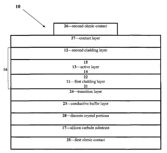
An understanding of the invention may be achieved
with reference to Figure 1, which is a cross-sectional
CA 02426718 2003-04-22
WO 02/37579 PCT/USO1/45636
-13-
schematic view of a semiconductor structure for an LED
according to the present invention.
The semiconductor structure, which is generally
designated at 10, includes a first cladding layer 11 of
AlXInyGa1_X_YN, where 0 <_ x <_ 1 and 0 <_ y _< 1 and (x _+ y) <
1. In a more specific embodiment, the first cladding
layer 11 is gallium-free, consisting essentially of an
aluminum indium nitride having the formula, AlXInz_XN,
where 0 < x <_ 1.
The semiconductor structure 10 also includes a
second cladding layer 12 of AlXInyGal-X-'yN, where 0 <_ x _< 1
and 0 _< y <_ 1 and (x + y) <_ 1, or in a more specific
embodiment, a gallium-free aluminum indium nitride
cladding layer 12 having the formula, AlXIn~_~N, where 0 <
x <_ 1.
As noted, the first cladding layer 11 and the second
cladding layer 12 preferably have opposite conductivity
types. That is, if the first cladding layer 11 is an n-
type layer, then the second cladding layer 12 is a p-type
layer, and vice-versa. The former embodiment is favored
over the latter. This convention with respect to
conductivity types is maintained throughout the
specification. As is known by those familiar with light
emitting devices, including structural layers of opposite
conductivity types facilitates forwarding biasing of the
device, which in turn promotes the recombinations that
produce the desired emissions.
An active layer 13 having the formula AlxInyGal-X_yN,
where 0 <_ x <_ 1 and 0 <- y <_ 1 and (x + y) <_ l, is
positioned between the first cladding layer 11 and the
CA 02426718 2003-04-22
WO 02/37579 PCT/USO1/45636
-14-
second cladding layer 12. In a more specific embodiment,
the active layer 13 is gallium-free, consisting
essentially of an aluminum indium nitride having the
formula, AlMIn1_xN, where 0 <_ x < 1.
As used herein, the term "layer" generally refers to
a single crystal epitaxial layer.
The active layer 13 may be either doped or undoped.
As is known to those familiar with Group III nitride
properties, the undoped material will generally be
intrinsically n-type. In particular, the first cladding
layer 11 and the second cladding layer 12 have respective
bandgaps that are each larger than the bandgap of the
active layer 13. As noted earlier, the Group III mole
fractions can be selected to provide these
characteristics.
In this regard, Figure 2 theoretically describes
bandgap energy versus lattice parameter. The triangular
region of Figure 2 represents the range of bandgap
energies available for Group III nitrides of aluminum,
indium, and gallium. Figure 2 reveals that for any
particular lattice parameter, eliminating gallium
maximizes the bandgap energy (i.e., the bandgap for an
aluminum indium nitride is approximated by the AlN-InN
segment).
As is also known to those familiar with
semiconductor structures-especially laser structures-in
order to enhance the capabilities of a device, the active
layer should desirably have a lower bandgap than the
adjacent cladding layers, and a higher refractive index
than the adjacent cladding layers. Such a structure
gives two benefits important for laser capability.
CA 02426718 2003-04-22
WO 02/37579 PCT/USO1/45636
-15-
First, if the active layer has the lowest bandgap, it
forms a quantum well into which carriers tend to fall.
This helps to enhance the laser effect. Second,
waveguiding occurs in the material that has the highest
refractive index in the structure. Accordingly, when the
bandgap of the active layer is less than that of the
adjacent layers and its refractive index is greater than
that of the adjacent layers, the lasing capabilities of
the device are enhanced.
Moreover, as known to those of ordinary skill in
this art, the composition of ternary and quaternary Group
IIT nitrides can affect both their refractive index and
their bandgap. Generally speaking, a larger proportion
of aluminum increases the bandgap and decreases the
refractive index. Thus, in preferred embodiments, in
order for the cladding layers 11 and 12 to have a bandgap
larger than the active layer 13 and a refractive index
smaller than the active layer 13, the cladding layers 11
and 12 preferably have a higher fraction of aluminum as
compared to the active layer 13. The larger bandgap of
the cladding layers 11 and 12 enhances the confinement of
carriers to the active layer 13, thereby increasing the
efficiency of the device. Similarly, the lower
refractive index of the heterostructure layers 11 and 12
causes the light to be confined in the active layer 13.
As previously noted, the recited variables (e.g., x
and y) refer to the structural layer they describe. That
is, the value of a variable with respect to one layer is
immaterial to the value of the variable with respect to
another layer. For example, in describing the
semiconductor structure, the variable x may have one
CA 02426718 2003-04-22
WO 02/37579 PCT/USO1/45636
-16-
value with respect to first cladding layer 11, another
value with respect to second cladding layer 12, and yet
another value with respect to active described layer 13.
As will also be understood by those of ordinary skill in
the art, the limitation 0 <_ (x _+ y) < 1 in the expression
AlXInyGai_X-yN simply requires that the Group III elements
and the nitrogen to be present in a 1:1 molar ratio.
Examples 1 and 2 (below) disclose various molar
ratios for the Group III nitrides in the cladding layers
and the active layer. In particular, Example 1 describes
a ternary InXAls_XN cladding layer composition for a blue
LED, and Example 2 describes a ternary InxAl1_XN active
layer composition for a blue LED:
Example 1
The cladding layers for a blue LED (425 nm c ~,c 480
nm) must have a band-gap energy greater than that of the
blue active layer (2.58 - 2.92 eV). For the ternary
InXAl1_XN, the bandgap energy of the ideal crystal remains
a matter of research and debate. This is primarily due
to the difficulty in growing high quality, uniform
epitaxial layers of the solid solution that are thick
enough (approximately 0.2 ~,m) for optical transmission
measurements to determine the bandgap energy. From
current data, Ino,l7Alo,83N has a bandgap energy of 2.9-3.0
25. eV. See S. Yamaguchi, M. Kariya, S. Nitta, T. Takeuchi,
C. Wetzel, H. Amano, and I. Akasaki, Appl. Phys. Lett. 76
876 (2000). Therefore, cladding layers for blue LEDs
should have an indium molar fraction of less than 0.17.
See K. S. Kim, A. Saxler, P. Kung, M. Razeghi, and K. Y.
Kim, Appl. Phys. Lett. 71 800 (1997).
CA 02426718 2003-04-22
WO 02/37579 PCT/USO1/45636
-17-
Example 2
Blue light emissions are produced for the ternary
InxAl1_xN between 0.14 < x < 0.21, with Ino,l7Alo.e3N
producing luminescence peaked at 450 nm and Ino,2~Alo,7sN at
500 nm. See S. Yamaguchi, M. Kariya, S. Nitta, T.
Takeuchi, C. Wetzel, H. Amano, and I. Akasaki, Appl.
Phys. Lett. 76 876 (2000). Reducing the indium molar
fraction to less than 0.14 will produce light at shorter
wavelengths, thereby permitting emissions of 425 nm. For
green emission (e. g., 500 < ~,< 575 nm), the indium molar
fraction should be between about 0.22 < x < 0.35.
It will be understood by those of skill in the art
that these are bulk emission values and that growth of
the material as quantum wells will produce quantum
confinement that will blue shift these emission
wavelengths.
It will be further appreciated by those of ordinary
skill in the art that, as used herein, the concept of one
layer being "between" two other layers does not
necessarily imply that the three layers are contiguous
(i.e., in intimate contact). Rather, as used herein the
concept of one layer being between two other layers is
meant to describe the relative positions of the layers
within the semiconductor structure. Similarly, as used
herein, the concept of a first layer being in contact
with a second layer, "opposite" a third layer, merely
describes the relative positions of the first and second
layers within the semiconductor structure.
That said, in preferred embodiments of the
semiconductor structure, the active layer 13 has a first
surface 14 contiguous to the first cladding layer 11 and
CA 02426718 2003-04-22
WO 02/37579 PCT/USO1/45636
-18-
a second surface 15 contiguous to the second cladding
layer 12. In other words, in such embodiments, the
active layer 13 is sandwiched directly between the first
cladding layer 11 and the second cladding layer 12, with
no additional layers disturbing this three-layer double
heterostructure, which is designated by the brackets 16.
The structural designation "double heterostructure"
is used herein in a manner well understood in this art.
Aspects of these structures are discussed, for example,
in Sze, Physics of Semiconductor Devices, Second Edition
(1981) at pages 708-710. Although the cited Sze
discussion refers to lasers, it nonetheless illustrates
the nature of, and the distinction between,
homostructure, single heterostructure, and double
heterostructure devices.
The semiconductor device 10 can further comprise a
silicon carbide substrate 1.7 that has the same
conductivity type as first cladding layer 11. The
silicon carbide substrate 17 preferably has a polytype of
3C, 4H, 6H, or 15R. The first cladding layer 11 is
positioned between the silicon carbide substrate 17 and
the active layer 13.
In another embodiment of the invention depicted by
Figure 3, the silicon carbide substrate 17 is in contact
with the first cladding layer 11, opposite the active
layer 13 (i.e., there are no intervening layers between
silicon carbide substrate 17 and first cladding layer
11) .
The silicon carbide substrate 17 is most preferably
a single crystal. As is well understood by those of
ordinary skill in this art, a high quality single crystal
CA 02426718 2003-04-22
WO 02/37579 PCT/USO1/45636
-19-
substrate provides a number of structural advantages that
in turn provide significant performance and lifetime
advantages. The silicon carbide substrate 17 can be
formed by the methods described in U.S. Pat. No.
4,866,005 (now U.S. Patent No. RE 34,861), which is
commonly assigned with the pending application.
Preferably, the silicon carbide substrate 17 and the
first cladding layer 11 are n-type because high-quality,
silicon carbide single crystal substrates have been
somewhat easier to produce as n-type.
In a preferred embodiment depicted by Figure 4, the
first cladding layer 11 has a first surface 21 that is in
contact with the silicon carbide substrate 17 and a
second surface 22 that is in contact with the active
layer 13. In particular, the composition of the first
cladding layer 11 is progressively graded such that the
crystal lattice at its first surface 21 more closely
matches the crystal lattice of the silicon carbide 17,
and the crystal lattice at its second surface 22 more
closely matches the crystal lattice of the active layer
13. A sufficient mole fraction of indium must be present
in the first cladding layer 11 to ensure that it remains
conductive at its first surface 21, adjacent to the
silicon carbide substrate 17.
As used herein, the concept of more closely matching
respective crystal lattices does not imply perfect
matching, but rather that a layer composition has been
progressively graded so that its lattice at a layer
interface is more compatible with the crystal lattice of
the adjacent layer. When fabricating devices, a number
of considerations must be balanced, one of which is
CA 02426718 2003-04-22
WO 02/37579 PCT/USO1/45636
-20-
lattice matching. If other factors are more important, a
perfect or close lattice match may be less important and
vice versa.
In this regard, cladding layers, especially aluminum
indium nitride cladding layers, can be selectively
lattice matched to gallium-containing active layers,
especially gallium nitride and indium gallium nitride
active layers, in order to reduce strain and defects. In
particular, aluminum indium nitrides are useful because
they can be lattice matched to other Group III nitrides
with higher bandgaps. See Figure 2.
As will be understood by those having ordinary skill
in the art, lattice matching of the cladding layers and
the active layer can be a one-sided lattice match (i.e.,
where a lattice match occurs on one side of the active
layer) or a two-sided lattice match (i.e., where a
lattice match occurs on both sides of the active layer).
In another embodiment depicted by Figure 5, the
semiconductor structure 10 further includes a conductive
buffer layer 23 positioned between the silicon carbide
substrate 17 and the first cladding layer 11. In a
variant of this embodiment, the conductive buffer layer
23 is sandwiched between the silicon carbide substrate 17
and the first cladding layer 11, with no intervening
layers. The conductive buffer layer 23 preferably
consists essentially of aluminum gallium nitride having
the formula Al~Ga1_xN, where 0 <_ x <_ 1. Alternatively,
when the first cladding layer 11 consists essentially of
aluminum indium nitride having the formula, AlXInl_XN,
where 0 c x <_ 1, the conductive buffer layer 23
preferably consists essentially of aluminum indium
CA 02426718 2003-04-22
WO 02/37579 PCT/USO1/45636
-21-
nitride having the formula, AlxIn~_XN, where 0 <_ x <_ 1.
Other acceptable buffers and buffer structures include
those described in commonly assigned U.S. Patent Nos.
5,523,589, 5,393,993, and 5,592,501, the contents of each
hereby being incorporated entirely herein by reference.
To facilitate the transition between the first
cladding layer 11 and the conductive buffer layer 23, the
semiconductor structure 10 can further include a Group
III nitride transition layer 24, preferably formed of a
compositionally graded layer that is positioned between
the conductive buffer layer 23 and the first cladding
layer 11. The transition layer 24 has the same
conductivity type as the first cladding layer 11 and the
silicon carbide substrate 17. See Figure 6.
Alternatively, as depicted by Figure 7, the
conductive buffer layer 23 and transition layer 24 can be
replaced by discrete crystal portions 28 (i.e., i.e.,
Group III nitride dots, preferably gallium nitride dots
or indium gallium nitride dots) separating the first
cladding layer 11 and the silicon carbide substrate 17.
In such an embodiment, the discrete crystal portions 28
are present in an amount sufficient to minimize or
eliminate the barrier between the first cladding layer 11
and the silicon carbide substrate 17, but less than the
amount that would detrimentally affect or destroy the
function of any resulting light emitting device formed on
the silicon carbide substrate 17.
Moreover, in another embodiment the discrete crystal
portions 28 may be positioned between the silicon carbide
substrate 17 and the conductive buffer layer 23. Figure
1 broadly illustrates the relative positions of the
CA 02426718 2003-04-22
WO 02/37579 PCT/USO1/45636
-22-
conductive buffer layer 23, the transition layer 24, and
the discrete crystal portions 28 when one of more of
these components are present in the semiconductor
structure.
The discrete crystal portions do not form an
epitaxial layer. Accordingly, those of ordinary skill in
the art will understand that the depiction of the
discrete crystal portions 28 in Figure 1 and Figure 7 is
merely schematic.
Preferably, the discrete crystal portions 28 are
formed from gallium nitride or indium gallium nitride.
The inclusion of such discrete crystal portions of
gallium nitride is disclosed more fully in commonly
assigned U.S. patent applications Serial Nos. 08/944,547,
filed October 7, 1997, for "Group III Nitride Photonic
Devices on Silicon Carbide Substrates with Conductive
Buffer Interlayer Structure," which is incorporated
entirely herein by reference.
In yet another embodiment, the semiconductor
structure 10 further includes a first ohmic contact 25
and a second ohmic contact 26. As indicated in Figure 1,
the first ohmic contact 25 is positioned in the
semiconductor structure such that the silicon carbide
substrate 17 is between the first ohmic contact 25 and
the first cladding layer 11. The second ohmic contact 26
is positioned in the semiconductor structure such that
the second cladding layer 12 is between the second ohmic
contact 26 and the active layer 13. See Figure 1.
The semiconductor structure 10 may further include a
Group III nitride contact layer 27 positioned between the
second ohmic contact 26 and the second claddin°g layer 12.
CA 02426718 2003-04-22
WO 02/37579 PCT/USO1/45636
-23-
The contact layer 27 and the second cladding layer 12
have the same conductivity type, typically p-type. See
Figure 1.
In preferred embodiments, the contact layer is p-
type and is made of gallium nitride(preferably magnesium-
doped gallium nitride); indium nitride; aluminum indium
nitride of the formula AlXIn1_XN, where 0 < x < 1; aluminum
gallium nitride of the formula AlXGa1_XN, where 0 < x < 1;
indium gallium nitride of the formula InXGal_xN, where 0 <
x < 1; or AlXInyGal_X_yN, where 0 < x < 1, and 0 < y < 1 and
(x + y) < 1. In this regard, the exclusion of both 0 and
1 from the range requires the presence of both Group III
elements in the alloy.
In a most preferred embodiment, the contact layer is
a p-type contact layer comprising a superlattice formed
from a plurality of Group III nitride layers selected
from the group consisting of gallium nitride (preferably
magnesium-doped gallium nitride); indium nitride;
aluminum indium nitride of the formula AlXInl_~N, where 0 <
x < 1; aluminum gallium nitride of the formula AlxGal_xN,
where 0 < x < 1; indium gallium nitride of the formula
InXGal_XN, where 0 < x < 1; and AlXInyGal_X_YN, where 0 < x <
1 and 0 < y < 1 and ( x + y ) < 1.
In particular, the superlattice is best formed from
alternating layers of any two of these Group III nitride
layers. In such a superlattice, alternating layers of
any two of gallium nitride, aluminum indium nitride, an
indium gallium nitride are most preferred
More generally, it is preferable to incorporate. in
the superlattice structure at least one layer of indium
nitride, aluminum indium nitride, indium gallium nitride,
CA 02426718 2003-04-22
WO 02/37579 PCT/USO1/45636
-24-
or aluminum indium gallium nitride (i.e., the
superlattice should not be formed from only gallium
nitride layers). Aluminum gallium nitride layers are
somewhat less favored. For example, a superlattice
formed from a plurality of contiguous p-type Group III
nitride layers selected from the group consisting of
gallium nitride, aluminum indium nitride, indium gallium
nitride is especially desirable, provided at least one
contiguous p-type Group III nitride layer is either
aluminum indium nitride or indium gallium nitride.
Preferably, the first ohmic contact 25 is placed
directly on the silicon carbide substrate 17, opposite
the first cladding layer 11, and the second ohmic contact
26 is placed directly on the Group III nitride contact
layer 27, opposite the second cladding layer 12. In a
variant of this embodiment, the contact layer 27 is
sandwiched between the second ohmic contact 26 and the
second cladding layer 12, with no intervening layers.
As recognized by those of ordinary skill in this
art, the buffer layer 23 provides a physical and
electronic transition between the silicon carbide
substrate 17 and the first cladding layer 11. In many
circumstances, the presence of the buffer layer 23 helps
ease the physical strain that can result from the lattice
differences between the silicon carbide substrate 17 and
the first cladding layer 11. Furthermore, to preserve
the vertical function of the device, the buffer layer 23
has to be sufficiently conductive to carry the desired or
required current to operate the device 10. Likewise, the
transition layer 24 serves a similar physical and
electronic transition.
CA 02426718 2003-04-22
WO 02/37579 PCT/USO1/45636
-25-
The ohmic contacts 25 and 26, which complete the
advantageous vertical structure of the invention, are
preferably formed of a metal such as aluminum (A1),
nickel (Ni), titanium (Ti), gold (Au), platinum (Pt),
vanadium (V), alloys, or blends thereof, or sequential
layers of two or more of these metals, but also may be
formed of other ohmic contact materials known by those
skilled in the art provided that they exhibit ohmic
character and do not otherwise interfere with the
structure or function of the ZED 10.
To the extent the ohmic contact 25 is formed to the
silicon carbide substrate 17, the invention is
distinguished from those devices that employ sapphire.
Sapphire cannot be made conductive, and so cannot be
connected to an ohmic contact. Consequently, sapphire-
based devices cannot be formed into the kinds of vertical
structures that are most preferred for ZEDS.
Accordingly, in one preferred embodiment the
invention is a semiconductor structure for light emitting
devices that includes a single crystal silicon carbide
substrate 17 of a 3C, 4H, 6H, or 15R polytype, an active
layer 13 of AlXInYGal-X-yl~, where 0 <_ x <_ 1 and 0 <_ y <_ 1
and (x + y) <_ 1, a gallium-free first cladding layer 11
consisting essentially of AlXIni_XN, where 0 G x <_ 1, and a
second cladding layer 12 of AlxInyGal_X_yN, where 0 <_ x <_ 1
and 0 <_ y <_ 1 and (x + y)
In another preferred embodiment, the invention is a
semiconductor structure for light emitting devices that
includes a single crystal silicon carbide substrate 17 of
a 3C, 4H, 6H, or 15R polytype, a gallium-free active
CA 02426718 2003-04-22
WO 02/37579 PCT/USO1/45636
-2 6-
layer 13 consisting essentially of AlXIns_xN, where 0 <_ x <
1, a first cladding layer 11 of AlxInyGa1_x_yN, where 0 <_ x
<_ 1 and 0 <_ y _< 1 and (x + y) <_ 1, and a second cladding
layer 12 of AlXInyGal_x_yN, where 0 <_ x <_ 1 and 0 <_ y _< 1
and (x + y) <_ 1.
In each of these embodiments, the first cladding
layer 11 is positioned between the silicon carbide
substrate 17 and the active layer 13, and the second
cladding layer 12 is positioned in the semiconductor
20 structure such that the active layer 13 is between the
first cladding layer 11 and the second cladding layer 12.
Moreover, as in the other disclosed embodiments of the
invention, the first cladding layer 11 and the silicon
carbide substrate 17 have the same conductivity type,
preferably opposite the conductivity type of the second
cladding layer 12. Finally, the respective bandgaps of
the first cladding layer 11 and the second cladding layer
12 are each larger than the bandgap of the active layer
13.
In either of these embodiments, the composition of
the first cladding layer 11 can be progressively graded
such that the crystal lattice at its first surface 21
more closely matches the crystal lattice of the silicon
carbide 17, and the crystal lattice at its second surface
22 more closely matches the crystal lattice of the active
layer 13.
Furthermore, and in accordance with the previous
descriptions, either of these preferred structures may
also include one or more of the following layers-the
conductive buffer layer 23, the Group III nitride
transition layer 24, the Group III nitride contact layer
CA 02426718 2003-04-22
WO 02/37579 PCT/USO1/45636
_27_
27, and the ohmic contacts 25 and 26. Ln this regard,
the conductive buffer layer 18 most preferably is
aluminum gallium nitride having the formula AlxGa1_XN,
where 0 <_ x 5 1, or aluminum indium nitride having the
formula AlxIn1_XN, where 0 <_ x <_ 1.
Tn the drawings and the specification, typical
embodiments of the invention have been disclosed.
Specific terms have been used only in a generic and
descriptive sense, and not for purposes of limitation.
The scope of the invention is set forth in the following
claims.