Note: Descriptions are shown in the official language in which they were submitted.
CA 02426909 2003-04-24
WO 02/44996 PCT/USO1/50161
INTEGRATED CIRCUIT FOR CONDITIONING AND CONVERSION OF
BI-DIRECTIONAL DISCRETE AND~ANALOG SIGNALS
FIELD OF 1NVENTION
The present invention relates to the field of programmable input and output
interfaces and in particular to an integrated circuit that can be programmed
to
accommodate various input/output signals with different characteristics at the
same
time and through the same interface.
1o BACKGROUND OF INVENTION
For any computer-controlled electrical system, the handling of input and
output between components of the system is an important aspect of the system.
An
interface between components of a system can convert or condition an output
signal
from one component to become a compatible input signal in another component.
This
conversion or conditioning must be performed while maintaining the signal's
integrity
and accuracy.
OFten, an input/output interface will have to coordinate input and output
signals with extremely varied signal characteristics. For example, one
component can
have analog signals that need to be converted into digital signals in order to
be
2o analyzed by another component. In another instance, typical for aircraft,
analog
signals from one component can have a. voltage range as great as (-15 to +28)
volts
while another component in the system has a voltage range of +/- 5 millivolts.
Other
situations entail having components that utilize both differential and single-
ended
signals that have to be input to another component.
Given the wide variety of signal characteristics that can exist within a given
system, input/output interface designs are typically developed to apply to a
specific
system. In particular, for systems on an aircraft, sensors on the aircraft can
produce
widely different output signals that have to be converted and conditioned in
order to
be processed by the aircraft computers. Typically, a different input/output
interface is
1
CA 02426909 2003-04-24
WO 02/44996 PCT/USO1/50161
developed for every sensor to produce a digital stream of data readable by the
aircraft
computers.
Redesigning the input/output interface every time a new sensor is used wastes
valuable time and money, as the designer must gain expertise with these
sensors
before designing the new interface. As such, there exists a need fox a compact
device
that can be easily incorporated into a component system and programmable to
handle
a multitude of signals of varied characteristics to create a single standard
interface
between components of that system.
1o SUMMARY OF THE INVENTION
This invention comprises a configurable integrated circuit (IC) which is
advantageously a single miniature chip to coordinate input and output (I/O)
signals.
The chip performs signal conditioning, analog-to-digital and digital-to-analog
conversion. Both single-ended signals and differential signals can be handled
at each
Z5 channel of the chip. In addition, each channel is configurable to accept
input signals
or generate output signals. This invention enables the reuse of Il0 hardware
across
multiple applications and reduces chip count, board space and connections and
thus
increases design reliability.
In one illustrative embodiment an input/output interface within a computer
2o controlled electrical system comprises a plurality of signal conditioning
cells to
provide a physical interface for electrical signals in the system where each
of the
plurality of signal conditioning cells is capable of handling signals with
different
characteristics. A signal conversion cell connected to the signal conditioning
cells is
capable of converting each of the electrical signals on the plurality of
channels to
25 become a digital data value for the computer. The plurality of signals
includes
discrete signals, analog signals, differential signals, or single-ended
signals.
2
CA 02426909 2003-04-24
WO 02/44996 PCT/USO1/50161
BRIEF DESCRIPTION OF THE DRAWINGS
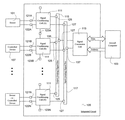
Figure 1 depicts a generic block diagram of an aircraft computer interfacing
with various sensors and controlled devices using an integrated circuit in
accordance
with an illustrative embodiment of our invention.
Figure 2 is a circuit diagram of a single conditioning cell in accordance with
one embodiment of our invention.
Figure 3 is a circuit diagram of a single conversion cell in accordance with
one
embodiment of our invention.
1o DESCRIPTION OF THE INVENTION
Figure 1 depicts a typical aircraft system in which our invention may be
employed. Sensors 101 on an aircraft produce continuously varying analog and
or on-
off discrete signals that need to be processed by the aircraft computer 103.
Each
sensor 101 can produce a signal that has different characteristics than other
sensors
because of the different types of sensors that are necessary to be on an
aircraft. An
integrated circuit 105 in accordance with our invention is interposed between
the
sensors 101 and the computer 103. The integrated circuit 105 can be installed
in
either the same line replaceable unit (LRI~ as the aircraft computer or in a
separate
'black box'. Each sensor 101 will transmit its signals to the integrated
circuit 105 that
2o conditions and converts the signals into a digital form that can be read by
the aircraft
computer 103. In turn, the aircraft computer 103 can send digital signals back
to the
integrated circuit 105. These signals will also be conditioned by the
integrated circuit
105 and then transmitted to other controlled devices 107 on the aircraft.
Figure 1 also depicts the layout of one illustrative embodiment of the
integrated circuit 105 of our invention. The physical implementation of the
integrated
circuit 105 is advantageously embodied as a single semiconductor chip, but any
other
similar implementation can be used.
3
CA 02426909 2003-04-24
WO 02/44996 PCT/USO1/50161
The integrated circuit 105 includes a number of signal conditioning cells
(11 lA to 111N) that each provide pairs of physical leads (121A to 121N) and
(122A
to 122N) to physically connect the integrated circuit with the various types
of signals
within the component system. Each signal conditioning cell 111 can be
configured by
the aircraft computer 103 to condition a number of different signal types as
described
below. The signal conditioning cells (111) condition each input signal by
buffering
the input signal characteristics .into standard signal characteristics, for
example -10
volt to + 10 volt, that can be converted by a shared analog to digital
converter 303,
shown in Figure 3. The signal conditioning cells 111 condition each output
signal by
to buffering a standard signal, for example -10 volt to + 10 volt, that is
provided by a
shared digital to analog converter 325 shown in Figure 3, into output signals
with
various signal characteristics. The signal conditioning cells 111 interface
with a
signal conversion cell 113 via an output multiplexor, for example a shared
output
analog signal bus 115 and an input multiplexor, for example a shared input
analog
signal bus 117. Signal conversion cell 113 includes registers that store
digital values
of the input and output signals and also configuration information for each of
the
signal conditioning cells 111. Signal conversion cell 113 also includes a
sequencer
and control module 343, shown in Figure 3, which organizes the interaction
among
the various internal cells of the integrated circuit 105.
2o Advantageously, an integrated circuit in accordance with our invention is
able
to accommodate both input signals and output signals. Figure 2 depicts a
signal
conditioning cell circuit that allows each channel to be programmed to accept
input
signals or produce output signals without affecting the signal. Physical leads
121 and
122 are connected to the inputs of an input amplifier 205 and connected
through
transmission gates to both a current driver 225 and a voltage driver 223. In
one
embodiment of the invention, the input amplifier 205 is an operational
amplifier and
the physical lead 121 is connected to its non-inverting (+) input and physical
lead 122
is connected to its inverting (-) input. Sequencer and control module 343
controls the
on-off setting of current driver transmission gate 234 based on values that
the aircraft
3o computer 103 has stored in the configuration register file 341, shown in
Figure 3.
4
CA 02426909 2003-04-24
WO 02/44996 PCT/USO1/50161
Sequencer and control module 343 controls the on-off setting of voltage driver
transmission gate 235 based on values that the aircraft computer 103 has
stored in the
configuration register file 34I. Voltage driver 223 can also be programmed to
function as a common mode voltage reference for a adjacent signal conditioning
cell
111 by supplying an output, for example to connection point 123A. When a
signal
conditioning cell is configured to receive an input, both the current driver
transmission gate 234 and the voltage driver transmission gate 235 are set
into high
impedance states by the sequencer and control module 343, shown in Figure 3.
When the signal on the signal-conditioning cell is to be output, the input
operational amplifier 205 is still activated and will have no effect on the
output signal.
Having the input still activated while producing an output signal allows the
invented
system to be self testing. Since the input is always connected to the final
output, the
input can be checked at any time to be certain that the output is functioning
properly.
Referring again to Figure. 2, the physical leads 121 and 122 interfacing with
the signal conditioning cell 111 of integrated circuit 105 are paired up to
create one
signal channel. Having two leads per signal channel is necessary in order to
be able
to accommodate both differential signals and single-ended signals. In addition
to
providing the physical leads, the signal conditioning cell 105 implements
circuitry to
be able to handle a number of different signal types. Input amplifier 205
buffers input
Zo voltage signals. Load resistor 20I is connected across physical leads 12I
and 122 via
transmission gates 232 and 233 to convert input current signals into a voltage
input
for input amplifier 205. In one embodiment of our invention, transmission
gates 232
and 233 are field effect transistors (FET) with "on" impedance of 190 ohms and
load
resistor 201 has a value of 620 ohms. Sequencer and control module 343
controls the
on-off setting of transmission gates 232 and 232 based on values that the
aircraft
computer 103 has stored in the configuration register file 341, shown in
Figure 3.
When the signal conditioning cell 105 is producing an output signal on
physical leads 121 and 122, this output signal is wrapped back for built-in
test
purposes and monitored as an additional input signal. All input signals are
treated as
5
CA 02426909 2003-04-24
WO 02/44996 PCT/USO1/50161
differential signal inputs. In instances where a single-ended signal is
utilized, for
example by an aircraft sensor, each signal conditioning cell 105 has a
transmission
gate 231 that allows one of the physical leads to be connected to a common
ground
point and an input 123, also shown in Figure l, that allows another signal
conditioning cell to provide a common mode voltage reference. By having two
leads
for the differential signal, the differential signal keeps its integrity and
the single-
ended signal has a reference to its local ground. Discrete signals are treated
as single-
ended analog signals thereby adding the benefits of programmable hysteresis
and
programmable debounce.
to Referring to Figure 1, signal conversion cell 113 will either receive the
input
signals from or transmit an output signal to each signal-conditioning cell
(111A to
111N). Referring back to Figure 3, for input signals from the signal selection
module,
The input operational amplifier 205 scales the signal to the full range
supported by an
analog to digital converter 303, shown in Figure 3, while maintaining signal
integrity
and accuracy. A programmable gain module 207 is connected across the non-
inverting input of input operational amplifier 205. In one embodiment, the
programmable gain module 207 is implemented as a system of resistors in
parallel
with transmission gates to switch them in or out of the circuit and vary the
feedback
resistance to determine the total gain according to the following formula:
RFeedback
2o Eq. (1 ) VouT = Rir,put Vir,put
The scaling step of the input operational amplifier 205 produces the maximum
resolution for a number of signal ranges using a single range converter. For
example,
the scaling range for the signals should be able to handle ranges, typically
found in
aircraft, as great as -15V to 28V signals.
The signal can also be filtered through optional programmable low-pass filter
209 after passing the input operational amplifier 205. The filtering of the
signal is
6
CA 02426909 2003-04-24
WO 02/44996 PCT/USO1/50161
used mainly as an anti-aliasing low pass filter that can be implemented by a
switched
capacitor network.
Advantageously, our invention includes an input signal multiplexor. For
example, after the signal optionally passes through the filter 209, it is
routed into a
multiplex transmission gate 241, which selectively determines when the signal
is
connected to the input analog signal bus 117 at connection point 127, as shown
in
Figure 1.
For output signals, either the current driver 225 or the voltage driver 223
can
be enabled. The voltage driver 223 amplifies the voltage at a variable gain
similar to
to the input operational amplifier 205. The current driver 225 has a set
number of
currents that can be selected when programmed. Output signals from both the
current
drivers and voltage drivers are presumed to be single-ended and reference to a
local
ground is provided as a signal return. An embodiment of the present invention
to
produce a differential signal uses two separate channels whereby one channel
carries
the true signal and the other carries the negative signal.
Figure 3 depicts the several components of the signal-conversion cell 113.
Before transmitting the input signal to the analog to digital converter module
303, the
signal conversion cell uses an input signal multiplexor, for example an input
analog
signal bus 117, shown in Figure l, and a sample and hold module 301 to prepare
the
2o various analog input signals to be converted by the converter module 303.
Input
analog signal bus 117 is connected to each signal-conditioning cell 111 of the
integrated circuit 105.
In one embodiment of the input signal multiplexor of our invention, the
sequencer and control module 343 routes analog data from a selected signal-
conditioning cell 111 by activating the multiplex transmission gate 241, shown
in
Figure 2, in that particular cell. The selected signal is routed from
connection point
127, via the input analog signal bus 117 and connection point 137 to the input
of a
sample and hold module 301. Sample and hold module 301 will sample a given
signal and will hold the signal's analog value to ensure that a stable
unchanging signal
7
CA 02426909 2003-04-24
WO 02/44996 PCT/USO1/50161
is available to an analog to digital converter 303. The analog to digital
converter 303
must have a stable analog input signal to ensure that proper conversion
occurs.
Analog to digital converters 303 convert the various analog signals to digital
values.
In one embodiment, the analog to digital converter has twelve bit precision.
A digital decoder 305 is used to map the various digital signals, after
conversion to digital format, to input register file 307 at an address
corresponding to
the appropriate signal conditioning cell 111. When the data to be latched is
placed on
a bus that feeds to the register file, the address of the selected register is
fed into the
decoder by the sequencer and controller 343. The decoder sends a signal to the
to selected register's enable, and the data is latched into that register.
The digital signals are first transmitted to a digital decoder 323 that parses
out
the digital signals from the input register file 321. The digital decoder 323
ensures
that only one output value at a time, stored in the registers is routed to the
digital to
analog converter 325. When the address of the selected register is fed into
the
decoder 323, the selected signal input is routed to the converter 325.
After digital to analog converter 325 converts the signal from a digital
format
to an analog format, the signal is routed via connection point 135 to an
output signal
multiplexor, for example the output analog signal bus, shown in Figure 1, and
to each
signal conditioning cell at connection point 125. The sequencer and control
module
343 then asserts a digital signal to the sample and hold module 221 of the
selected
signal conditioning cell (111A to 111N) that will then hold the analog signal
value
present on the output analog signal bus.
Advantageously, the combination of transmission gates 241, an analog input
analog signal bus 117, a sample and hold module 301 and a digital decoder 305
for
the input path and the corresponding combination of digital decoder 323,
output
analog signal bus 115, and sample and hold modules 221 for the output path
allow a
reduction in the amount of analog to digital converters 303 and digital to
analog
converters 325 utilized, which saves space in the compact general purpose
interface
integrated circuit 105. Instead of implementing a separate converter for each
physical
8
CA 02426909 2003-04-24
WO 02/44996 PCT/USO1/50161
input/output channel, the signals are multiplexed and controlled to allow one
converter to be used for multiple channels.
From the internal registers of the converters, the data is placed or taken
from
the integrated circuit's register files 307 and 321. The register files 307
represent the
interface to the chip from the computer 103. Three groups of register files
are needed
for input data, output data and configuration data. The number of registers
per file
depends on the number of signals the chip is designed to handle. The size of
each
register depends on the accuracy of the conversion logic. For twelve-bit
precision, a
register with twelve-bit memory capacity is needed.
to Reading the input register file can access values associated with samples
of
input signals. The aircraft computer will be able to access the information
from the
sensors 101 by accessing these input registers. To output information through
the
invented system, the aircraft computer 103 can write the data to the output
register
file.
Advantageously, the double-buffering system described above using aircraft
computer internal system files and the interface register files of the present
invention
is useful for asynchronous access to the chip to ensure stability of the
sampled values
before processing them or being read out of the chip. A further embodiment of
our
invention allows the aircraft computer to also directly access the analog to
digital
2o converter's registers and the digital to analog converter's registers.
The configuration register file 341 stores the gain and type of conditioning
for
each signal. Using the values stored in the configuration file register, the
sequencer
and control module 343 can organize the interaction among the internal modules
and
handle the mapping of the internal registers of the converters. The sequencer
and
control module 343 can also reconfigure the modules and control access to
input
register file 321 and output register file 307. The sequencer and control
module 343
ensures the correct order of internal operations and the synchronization of
the input
and output data streams.
9
CA 02426909 2003-04-24
WO 02/44996 PCT/USO1/50161
The present invention is not to be considered limited in scope by the
preferred
embodiments described in the specification. hdditional advantages and
modifications, which will readily occur to those skilled in the art from
consideration
of the specification and practice of the invention, are intended to be within
the scope
and spirit of the following claims.