Note: Descriptions are shown in the official language in which they were submitted.
CA 02427369 2003-04-29
METHODS AND APPARATUS FOR CONTROLLING POWER TO
ELECTRICAL CIRCUITRY OF A WIRELESS COMMUNICATION DEVICE
HAVING A SUBSCRIBER IDENTITY MODULE (SIM) INTERFACE
BACKGROUND
Field of the Technolo~y
The present application relates generally to wireless communication devices,
and
relates more particularly to controlling power to electrical circuitry of a
wireless
communication device having a Subscriber Identity Module (SIM) interface.
Description of the Problem
Minimizing power consumption of battery-operated portable wireless
communication devices, such as mobile stations operating in cellular
telecommunication networks, is a relatively important objective. Such devices
typically
include a radio frequency (RF) transceiver for communications and provide one
or more
functions for an end user, such as telephone, e-mail, text messaging,
calendaring/scheduling, and other organizing applications. The e-mail,
calendaring,
and/or organizing capabilities in the wireless device may be provided with a
wireless
synchronizing capability with a remote computer or other device.
Such devices typically include manual switches to power the device ON or OFF
in its entirety. With an ON/OFF switch, the battery of the device can be
conserved
when the device is not needed for direct use by the end user. Recently,
devices have
been becoming more mufti-functional in nature, providing for more than one of
the
1
CA 02427369 2003-04-29
above functions, for example. Some of these devices are known to provide
manual
switches to place them into an intermediate ON/OFF state where the wireless
capability is powered down but same other portions of the circuitry (e.g. the
microprocessor) are still generally active. Here, an end user can utilize
other
applications on the device (e.g. a local calendaring application) when the I~F
transceiver
is not needed. However, devices having this capability do not utilize a
Subscriber
Identify Module (SIM) interface in connection therewith.
Some wireless devices operate using a SIM which is connected to or inserted
into
the device at its SIM interface. A SIM is one type of a conventional "smart
card" used to
identify an end user (or subscriber) of the wireless device and to personalize
the device,
among other things. It generally includes a processor and memory for storing
information. Without a SIM, some wireless devices are not fully operational
for
communicating through particular wireless networks. By inserting a SIM into
the
device, an end user can have access to any and all of his/her subscribed
services. To
identify the subscriber, a SIM typically contains some user parameters such as
an
International Mobile Subscriber Identity (IMSI). In addition, a SIM is
typically
protected by a four-digit Personal Identification Number (PIN) which is stored
therein
and known only by the end user. An advantage of using the SIM is that end
users are
not necessarily bound by any single physical wireless device. Typically, the
only
element that personalizes a wireless device terminal is a SIM card. Therefore,
the user
2
CA 02427369 2003-04-29
can access subscribed services using any wireless device equipped to operate
with the
user's SIM.
Accordingly, there is a need for alternative methods and apparatus for
controlling power to electrical circuitry of a wireless communication device
having a
SIM interface, especially in a multi-functional device.
SUMMARY
Methods and apparatus for controlling power to electrical circuitry of a
wireless
communication device having a Subscriber Identify Module (SIM) interface are
described. In one illustrative example, a method includes the acts of
receiving a power
down signal from a user interface of the wireless communication device;
powering
down radio frequency (RF) transceiver circuitry of the wireless communication
device
in response to the power down signal; and maintaining power to a SIM interface
of the
wireless communication device while the RF transceiver circuitry is powered
down
from the power down signal. Advantageously, an end user of the wireless device
may
access stored information on a SIM while the wireless device is kept in this
low power
state with its RF transceiver circuitry being powered down.
BRIEF DESCRIPTION OF THE DRAWINGS
Embodiments of present invention wiil now be described by way of example
with reference to attached figures, wherein.
3
CA 02427369 2003-04-29
FIG. 1 is a block diagram of a communication system which includes a wireless
communication device for communicating in a wireless communication network,
where
the wireless communication device includes a smart card interface such as a
Subscriber
Identity Module (SIM) interface;
FIG. 2 is an illustration of the wireless communication network having the
wireless communication device operating therein for communicating data between
one
or more application servers through a public or private communication network;
FIG. 3 is a particular structure of a system for communication with the
wireless
communication device;
FIG. 4 is a more detailed example of a wireless communication device which has
a smart card interface (e.g. a SIM interface);
FIG. 5 is a state transition diagram for the wireless communication device of
FIG.
1 or FIG. 4; and
FIG. 6 is a flowchart which describes a method of controlling power to
circuitry
of the wireless communication device of FIG. i or FIG. 4.
DETAILED DESCRIPTION OF THE PREFERRED EMBODIMENTS
Broadly, a power down signal is received from a user interface of a wireless
communication device. In response, radio frequency (RF) transceiver circuitry
of the
wireless device is powered down. However, power is maintained to a SIM
interface of
the wireless device while the RF transceiver circuitry is powered down from
the power
4
CA 02427369 2003-04-29
down signal. Advantageously, an end user of the wireless device may access
stored
information on a SIM while the wireless device is kept in the low power state
with its
IZF transceiver circuitry powered down. Further advantageous implementation
details
are described below.
FIG. 1 is a block diagram of a communication. system 100 which includes a
wireless communication device 102 which communicates through a wireless
communication network 104. Wireless communication device 102 preferably
includes a
visual display 112, a keyboard 114, and perhaps one or more auxiliary user
interfaces
(UI) 116, each of which are coupled to a controller 106. Controller 106 is
also coupled to
radio frequency (RF) transceiver circuitry 108 and an antenna 110.
In most modern communication devices, controller 106 is embodied as a central
processing unit (CPU) which runs operating system software in a memory
component
(not shown). Controller 106 will normally control overall operation of
wireless device
102, whereas signal processing operations associated with communication
functions are
typically performed in RF transceiver circuitry 108. Controller 106 interfaces
with
device display 112 to display received information, stored information, user
inputs, and
the like. Keyboard 114, which may be a telephone type keypad or full
alphanumeric
keyboard, is normally provided for entering data for storage in wireless
device 102,
information for transmission to network 104, a telephone number to place a
telephone
call, commands to be executed on wireless device 102, and possibly other or
different
user inputs.
5
CA 02427369 2003-04-29
Wireless device 102 sends communication signals to and receives communication
signals from network 104 over a wireless link via antenna 110. RF transceiver
circuitry
108 performs functions similar to those of base station 120, including for
example
modulation/demodulation and possibly encoding/decoding and
encryption/decryption. It is also contemplated that RF transceiver circuitry
108 may
perform certain functions in addition to those performed by base station 120.
It will be
apparent to those skilled in art that RF transceiver circuitry 108 will be
adapted to
particular wireless network or networks in which wireless device 102 is
intended to
operate.
When wireless device 102 is fully operational, an RF transmitter of RF
transceiver
circuitry 108 is typically keyed or turned on only when it is sending to
network, and is
otherwise turned off to conserve resources. Such intermittent operation of
transmitter
has a dramatic effect on power consumption of wireless device 102. Since power
of
wireless device 102 is normally provided by a limited power source, such as a
rechargeable battery, device design and operation must minimize power
consumption
in order to extend battery life or time between power source charging
operations.
Similarly, an RF receiver of RF transceiver circuitry 108 is typically
periodically turned
off to conserve power until it is needed to receive signals or information (if
at all)
during designated time periods.
Wireless device 102 operates using a Subscriber Identity Module (SIM) which is
connected to or inserted in wireless device 102 at a SIM interface 142. SIM
140 is one
6
CA 02427369 2003-04-29
type of a conventional "smart card°° used to identify an end
user (or subscriber) of
wireless device 102 and to personalize the device, among other things. Without
SIM
140, the wireless device terminal is not fully operational for communication
through
wireless network 104. By inserting SIM 140 into wireless device 102, an end
user can
have access to any and all of his/her subscribed services. In order to
identify the
subscriber, SIM 140 contains some user parameters such as an International
Mobile
Subscriber Identity (IMSI). In addition, SIM 140 is typically protected by a
four-digit
Personal Identification Number (PIN) which is stored therein and known only by
the
end user. An advantage of using SIM 140 is that end users are not necessarily
bound by
any single physical wireless device. Typically, the only element that
personalizes a
wireless device terminal is a SIM card. Therefore, the user can access
subscribed
services using any wireless device equipped to operate with the user's SIM.
SIM and interfacing standards are well-known and defined, for example, in GSM
11.11 (SIM protocols), ISO/IEC 7816-1 (physical characteristics), ISG/IEC 7816-
2
(dimensions and locations of contacts), and ISO/IEC 7816-3 (electronic signals
and
transmission protocols). SIM 140 generally includes a processor and memory for
storing information. For interfacing with a standard GSM device having SIM
interface
142, a conventional SIM 140 has six (6) connections. A typical SIM 140 stores
all of the
following information: (1) an International Mobile Subscriber Identity (IMSI);
(2) an
individual subscriber's authentication key (Ki); (3) a ciphering key
generating algorithm
(A8) -- with Ki and BAND it generates a 64-bit key (Kc); (4) an authentication
algorithm
7
CA 02427369 2003-04-29
(A3) -- with Ki and RAND it generates a 32-bit signed response (SRED); (5) a
user PIN
code (1 & 2); (6) a PUK code (1 & 2) (this is also referred to as the SPIN);
(~) a user phone
book; (8) stored Short Message Service (SMS) messages; and (9) a preferred
network list.
SIM 140 rnay store additional user information for the wireless device as
well, including
datebook (or calendar) information and recent call information. As apparent,
some of
the information stored on SIM 140 (e.g. address book information and SMS
messages) is
initially received at wireless device 102 over wireless network 104 through
its RF
transceiver circuitry 108, or received from the end user through keyboard 114.
Another type of smart card is used in connection with a Universal Mobile
Telecommunications System (UMTS) standard. The UMTS standard does not restrict
the functionality of the wireless device eguipment in any way. Wireless device
terminals operate as the "air interface" and can have many different types of
identities.
Most of the UMTS identity types are borrowed directly from GSM specifications:
(1) an
International Mobile Subscriber Identity (IMSI); (2) a Temporary Mobile
Subscriber
Identity (TMSI); (3) a Packet Temporary Mobile Subscriber Identity (P-TMSI);
(4) a
Temporary Logical Link Identity (TLLI); (5) a mobile station ISDN (MSISDN);
(5) an
International Mobile Station Equipment Identity (IMEI); and (6) an
International Mobile
Station Equipment Identity and Software Number (IMEISV). A UMTS card has same
physical characteristics as a GSM SIM card. The UMTS card has several
functions: (1)
to support of one User Service Identity Module (USIM) application (optionally
more
than one); (2) to support of one or more user profiles on the USIM; (3) update
USIM
8
CA 02427369 2003-04-29
specific information over-the-air; (4) to provide security functions; (5) to
provide user
authentication; (6) to optionally provide for payment methods; and (7) to
optionally
provide for the secure downloading of new applications.
Some information stored on SIM 140 (e.g. address book and SMS messages) may
be retrieved and visually displayed on display 112. Wireless device 102 has
one or
more software applications which are executed by controller 144 to facilitate
the
information stored on SIM 140 to be displayed on display 112. Controller 144
and SIM
interface 142 have data and control lines 144 coupled therebetween to
facilitate the
transfer of the information between controller 144 and SIM interface 142 so
that it may
be visually displayed. An end user enters user input signals at keyboard 114, -
for
example, and in response, controller 144 controls SIM interface 142 and SIM
140 to
retrieve the information for display. The end user may also enter user input
signals at
keyboard 114, for example, and, in response, controller 144 controls SIM
interface 142
and SIM 140 to store information on SIM 140 for later retrieval and viewing.
Preferably,
the software applications executed by controller 106 include an application to
retrieve
and display address book information stored on SIM 140, and an application to
retrieve
and display SMS message information stored on SIM 140.
Wireless device 102 includes a battery interface 134 for receiving one or more
rechargeable batteries 132. Battery 132 provides electrical power to (most if
not all)
electrical circuitry in wireless device 102, and battery interface 132
provides for a
mechanical and electrical connection for battery 132. Battery interface 132 is
coupled to
9
CA 02427369 2003-04-29
a regulator 136 which regulates power to RF transceiver circuitry 108. Battery
interface
134 is also coupled to a separate regulator 146 which regulates power to SIM
interface
142 of wireless device 102. Regulator 146 may be the same regulator used to
regulate
power to most of the remaining circuitry of wireless device 102 (e.g.
controller 106 and
the user interface). Controller 106 is coupled to regulator 136 via a control
line 138 to
enable or disable power to RF transceiver circuitry 108. Similarly, controller
106 is
coupled to regulator 146 via a control line 148 to enable or disable power to
SIM
interface 142. Alternatively, line 148 is not such a control line, but rather
is a line which
supplies power to both SIM interface 142 and controller 106 (and any other
necessary
circuitry).
As apparent from the above, the term '°wireless device" is used
herein in
reference to a wireless mobile communication device. In the embodiment of FIG.
1,
wireless device 102 is referred to as mobile equipment which, when used with
SIM 140,
is referred to as a mobile station. Wireless device 102 may consist of a
single unit, such
as a data communication device, a cellular telephone, a multiple-function
communication device with data and voice communication capabilities, a
personal
digital assistant (PDA) enabled for wireless communication, or a computer
incorporating an internal modem. Alternatively, wireless device 102 may be a
multiple-
module unit comprising a plurality of separate components, including but in no
way
limited to a computer or other device connected to a wireless modem. In
particular, for
example, in the wireless device block diagram of FIG. 1, RF transceiver
circuitry 108 and
CA 02427369 2003-04-29
antenna 110 may be implemented as a radio modem unit that may be inserted into
a
port on a laptop computer. In this case, the laptop computer would include
display
112, keyboard 114, one or more auxiliary UIs 116, and controller 106 embodied
as the
computer's CPU. It is also contemplated that a computer or other equipment not
normally capable of wireless communication may be adapted to connect to and
effectively assume control of RF transceiver circuitry 108 and antenna 110 of
a single-
unit device such as one of those described above. Such a, wireless device 102
may have
a more particular implementation as described later in relation to wireless
device 402 of
FIG. 4.
Wireless device 102 communicates in and through wireless communication
network 104. In the embodiment of FIG. 1, wireless network 104 is a Global
Systems for
Mobile (GSM) and General Packet Radio Service (GPRS) network. Wireless network
104 includes a base station 120 with an associated antenna tower 118, a Mobile
Switching Center (MSC) 122, a Home Location Register (HLR) 132, a Serving
General
Packet Radio Service (GPRS) Support Node (SGSN) 126, and a Gateway GPRS
Support
Node (GGSN) 128. MSC 122 is coupled to base station 120 and to a landline
network,
such as a Public Switched Telephone Network (PSTN) 124. SGSN 126 is coupled to
base
station 120 and to GGSN 128, which is in turn coupled to a public or private
data
network 130 (such as the Internet). HLR 132 is coupled to MSC 122, SGSN 126,
and
2o GGSN 128.
11
CA 02427369 2003-04-29
Base station 120, including its associated controller and antenna tower 118,
provides wireless network coverage for a particular coverage area commonly
referred
to as a "cell". Base station 120 transmits communication signals to and
receives
communication signals from wireless devices within its cell via antenna tower
118.
Base station 120 normally performs such functions as modulation and possibly
encoding and/or encryption of signals to be transmitted to the wireless device
in
accordance with particular, usually predetermined, communication protocols and
parameters, under control of its controller. Base station 120 similarly
demodulates and
possibly decodes and decrypts, if necessary, any communication signals
received from
wireless device 102 within its cell. Communication protocols and parameters
may vary
between different networks. For example, one network may employ a different
modulation scheme and operate at different frequencies than other networks.
The wireless link shown in communication system 100 of FIG. 1 represents one
or more different channels, typically different radio frequency (RF) channels,
and
associated protocols used between wireless network 104 and wireless device
102. An
RF channel is a limited resource that must be conserved, typically due to
limits in
overall bandwidth and a limited battery power of wireless device 102. Those
skilled in
art will appreciate that a wireless network in actual practice may include
hundreds of
cells, each served by a distinct base station 120 and transceiver, depending
upon desired
overall expanse of network coverage. All base station controllers and base
stations may
12
CA 02427369 2003-04-29
be connected by multiple switches and routers (not shown), controlled. by
multiple
network controllers.
For all wireless device's 102 registered with a network operator, permanent
data
(such as wireless device 102 user's profile) as well as temporary data (such
as wireless
device's 102 current location) are stored in HLR 132. In case of a voice call
to wireless
device 102, HLR 132 is queried to determine the current location of wireless
device 102.
A Visitor Location Register (VLR) of MSC 122 is responsible for a group of
location
areas and stores the data of those wireless devices that are currently in its
area of
responsibility. This includes parts of the permanent wireless device data that
have been
transmitted from HLR 132 to the VLR for faster access. However, the VLR of MSC
122
may also assign and store local data, such as temporary identifications.
Optionally, the
VLR of MSC 122 can be enhanced for more efficient co-ordination of GPRS and
non-
GPRS services and functionality (e.g. paging for circuit-switched calls which
can be
performed more efficiently via SGSN 126, and combined GPRS and non-GPRS
location
updates).
Being part of the GPRS network, Serving GPRS Support Node (SGSN) 126 is at
the same hierarchical level as MSC 122 and keeps track of the individual
locations of
wireless devices. SGSN 126 also performs security functions and access
control.
Gateway GPRS Support Node (GGSN) 128 provides interworking with external
packet-
switched networks and is connected with SGSNs (such as SGSN 126) via an IP-
based
GPRS backbone network. SGSN 126 performs authentication and cipher setting
13
CA 02427369 2003-04-29
procedures based on the same algorithms, keys, and criteria as in existing
GSM. In
conventional operation, cell selection may be performed autonomously by
wireless
device 102 or by base station 120 instructing wireless device 102 to select a
particular
cell. Wireless device 102 informs wireless network 104 when it reselects
another cell or
group of cells, known as a routing area.
In order to access GPRS services, wireless device 102 first makes its presence
known to wireless network 104 by performing what is known as a GPRS "attach".
This
operation establishes a logical link between wireless device 102 and SGSN 126
and
makes wireless device 102 available to receive, for example, pages via SGSN,
notifications of incoming GPRS data, or SMS messages over GPRS. In order to
send and
receive GPRS data, wireless device 102 assists in activating the packet data
address that
it wants to use. This operation makes wireless device 102 known to GGSN 128;
interworking with external data networks can thereafter commence. User data
may be
transferred transparently between wireless device 102 and the external data
networks
using, for example, encapsulation and tunneling. Data packets are equipped
with
GPRS-specific protocol information and transferred between wireless device 102
and
GGSN 128.
As apparent from the above, the term "network" is used herein to denote fixed
portions of the network, including RF transceivers, amplifiers, base station
controllers,
network servers, and servers connected to network. Those skilled in art will
appreciate
that a wireless network may be connected to other systems, possibly including
other
14
CA 02427369 2003-04-29
networks, not explicitly shown in FIG. 1. A network will normally be
transmitting at
very least some sort of paging and system information on an ongoing basis,
even if
there is no actual packet data exchanged. Although the network consists of
many parts,
these parts all work together to result in certain behaviours at the wireless
link.
The above described electrical configuration for Tireless device 102 may be
used
to operate wireless device 102 as follows. In a first operational state of
wireless device
102, wireless device 102 is fully operative where regulators 136 and 146 are
enabled and
supplying power to RF transceiver circuitry 108 and SIM interface 142,
respectively. In
a second operational state of wireless device 102, wireless device 102 is only
partially
operative where regulator 136 is disabled by controller 106 so that RF
transceiver
circuitry 108 is powered off or shut down. However, regulator 146 continues to
be
operative and supply power to SIM interface 142 (and perhaps controller 106
and the
user interface). No wireless or RF communication is possible in the second
operational
state, but wireless device 102 consumes less power compared to the first
operational
state. In a non-operational state of wireless device 102, (most if not) all
electrical
circuitry of wireless device 102 including RF transceiver circuitry 108, SIM
interface 142,
and controller 106 are powered down. 'These state transitions may be
controlled by the
end user at the user interface. The above operation of wireless device 102 is
described
in more detail later in relation to FIG. 5.
FIG. 2 is a simplified illustration of wireless network 104 having wireless
device
102 operating therein for communicating data between one or more application
servers
CA 02427369 2003-04-29
202 through a public or private communication network 130. Network 130 may be
or
include Internet, and include a serving network to facilitate the
communication of
information between application servers 202 and wireless device 102. There are
three
application servers 202 shown in FIG. 2, namely, application servers 204, 206,
and 208;
however any suitable number of application servers may be employed in the
network.
Application servers 202 may provide any suitable voice and/or data services)
for
wireless device 102, especially "push"-based services. More specifically,
application
servers 202 may provide an electronic mail (e-mail) service, a wireless
application
protocol (WAP) service, a short messaging service (SMS) service, or an
application-
specific service such as a weather update service, a horoscope service, and a
stock
market quotation service, as a few examples. Some of this information, as well
as other
types of information, may be stored on SIM 140 (FIG. 1) of wireless device 102
after
being received by RF transceiver circuitry 108 (FIG. 1) and is retrievable as
described
above in relation to FIG. 1 and FIG. 5 as described below.
FIG. 3 shows a particular system structure for communicating with a wireless
communication device. In particular, FIG. 3 shows basic components of an IP-
based
wireless data network, such as a GPRS network. A wireless device 100
communicates
with a wireless packet data network 145, and may also be capable of
communicating
with a wireless voice network (not shown). Preferably, wireless network 145
provides
for "push"-based services to wireless device 100 and other similar devices.
Wireless
device 100 of FIG. 3 may be wireless device 102 of FIGs. 1 and 2. The voice
network
16
CA 02427369 2003-04-29
may be associated with IP-based wireless network 145 similar to, for example,
GSM and
GPRS networks, or alternatively may be a completely separate network. The GPRS
IP-
based data network is unique in that it is effectively an overlay on the GSM
voice
network. As such, GPRS components will either extend existing GSM components,
such as base stations 320, or require additional components to be added, such
as an
advanced Gateway GPRS Service Node {GGSN) as a network entry point 305.
As shown in FIG. 3, a gateway 140 may be coupled to an internal or external
address resolution component 335 and one or more network entry points 305.
Data
packets are transmitted from gateway 140, which is source of information to be
transmitted to wireless device 100, through network 145 by setting up a
wireless
network tunnel 325 from gateway 140 to wireless device 100. In order to create
this
wireless tunnel 325, a unique network address is associated with wireless
device 100. In
an IP-based wireless network, however, network addresses are normally not
permanently assigned to a particular wireless device 100 but instead are
dynamically
allocated on an as-needed basis. It is thus preferable for wireless device 100
to acquire a
network address and for gateway x.40 to determine this address so as to
establish
wireless tunnel 325.
Network entry point 305 is generally used to multiplex and demultiplex amongst
many gateways, corporate servers, and bulk connectiions such as the Internet,
for
example. There are normally very few of these network entry points 305, since
they are
also intended to centralize externally available wireless network services.
Network
17
CA 02427369 2003-04-29
entry points 305 often use some form of an address resolution component 335
that
assists in address assignment and lookup between gateways and wireless
devices. In
this example, address resolution component 335 is shown as a dynamic host
configuration protocol (DHCP) as one method for providing an address
resolution
mechanism.
A central internal component of wireless data network 345 is a network roister
315. Normally, network roisters 315 are proprietary to the particular network,
but they
could alternatively be constructed from standard commercially available
hardware. The
purpose of network roisters 315 is to centralize thousands of base stations
320 normally
implemented in a relatively large network into a central location for a long-
haul
connection back to network entry point 305. In some networks there may be
multiple
tiers of network roisters 315 and cases where there are master and slave
network roisters
315, but in all such cases the functions are similar. ~ften network roister
315 will access
a name server 307, in this case shown as a dynamic name server (DNS) 30~ as
used in
the Internet, to look up destinations for routing data messages. Base stations
320, as
described above, provide wireless links to wireless devices such as wireless
device 100.
Wireless network tunnels such as a wireless tunnel 325 are opened across
wireless network 345 in order to allocate necessary memory, routing, and
address
resources to deliver IP packets. In GPRS, such tunnels 325 are established as
part of
what are referred to as "PDP contexts"' (i.e. data sessions). To open wireless
tunnel 325,
wireless device 100 must use a specific technique associated with wireless
network 345.
18
CA 02427369 2003-04-29
The step of opening such a wireless tunnel 325 may require wireless device 100
to
indicate the domain, or network entry point 305 with which it wishes to open
wireless
tunnel 325. In this example, the tunnel first reaches network router 315 which
uses
name server 307 to determine which network entry point 305 matches the domain
provided. Multiple wireless tunnels can be opened from one wireless device 100
for
redundancy, or to access different gateways and services on the network. Once
the
domain name is found, the tunnel is then extended to network entry point 305
and
necessary resources are allocated at each of the nodes along the way. Network
entry
point 305 then uses the address resolution (or DI-1CP 335) component to
allocate an IP
address for wireless device 100. When an IP address has been allocated to
wireless
device 100 and communicated to gateway 140, information can then be forwarded
from
gateway 140 to wireless device 200.
Wireless tunnel 325 typically has a limited life, depending on wireless
device's
100 coverage profile and activity. Wireless network 145 will tear down
wireless tunnel
325 after a certain period of inactivity or out-~of-coverage period, in order
to recapture
resources held by this wireless tunnel 325 for other users. The main reason
for this is to
reclaim the IP address temporarily reserved for wireless device 100 when
wireless
tunnel 325 was first opened. Once the IP address is lost and wireless tunnel
325 is torn
down, gateway 140 loses all ability to initiate IP data packets to wireless
device 100,
whether over Transmission Control Protocol (TCP) or over User Datagram
Protocol
(UDP)
19
CA 02427369 2003-04-29
In this application, the expression °'IP-based wireless network" is
intended to
include, but is not limited to: (1) Code Division Multiple Access (CDMA)
network that
has been developed and operated by Qualcomm; (2) General Packet Radio Service
(GPRS) for use in conjunction with Global System for Mobile Communications
(GSM)
network both developed by standards committee of European Conference of Postal
and
Telecommunications Administrations (CEPT ); and (3) future third-generation
(3G)
networks like Enhanced Data rates for GSM Evolution (EDGE) and Universal
Mobile
Telecommunications System (UMTS). GPRS is a data communications overlay on top
of GSM wireless network. It is to be understood that although particzzlar IP-
based
wireless networks have been described, the communication re-establishment
schemes
of the present application could be utilized in any suitable type of wireless
packet data
network.
FIG. 4 is a detailed block diagram of a wireless communication device 402.
Wireless device 402 is preferably a two-way communication device having at
least voice
and data communication capabilities, including the capability to communicate
with
other computer systems. Depending on the functionality provided by wireless
device
402, it may be referred to as a data messaging device, a two-way pager, a
cellular
telephone with data messaging capabilities, a wireless Internet appliance, or
a data
communication device (with or without telephony capabilities).
If wireless device 402 is enabled for two-way communication, it will normally
incorporate a communication subsystem 411, which: includes a receiver 412, a
CA 02427369 2003-04-29
transmitter 414, and associated components, such as one or more (preferably
embedded
or internal) antenna elements 416 and 418, local oscillators (LOs) 413, and a
processing
module such as a digital signal processor (DSP) 420. Communication subsystem
411 is
analogous to RF transceiver circuitry 108 and antenna 110 shown in FIG. 1. As
will be
apparent to those skilled in field of communications, particular design of
communication subsystem 411 depends on the comaxtunication network in which
wireless device 402 is intended to operate.
Network access requirements will also vary depending upon type of network
utilized. In GPRS networks, for example, network access is associated with a
subscriber
or user of wireless device 402. A GPRS device therefore requires a Subscriber
Identity
Module, commonly referred to as a "SIM'° card 45&, in order to operate
on the GPRS
network. Without such a SIM card 456, a GPRS device will not be fully
functional.
Local or non-network communication functions (if any) may be operable, but
wireless
device 610 will be unable to carry out any functions involving communications
over the
I5 network.
When required network registration or activation procedures have been
completed, wireless device 402 may send and receive communication signals over
the
network. Signals received by antenna 416 through the network are input to
receiver
412, which may perform such common receiver functions as signal amplification,
frequency down conversion, filtering, channel selection, and like, and in
example
shown in FIG. 4, analog-t~-digital (A/D) conversion. l~/D conversion of a
received
21
CA 02427369 2003-04-29
signal allows more complex communication functions such as demodulation and
decoding to be performed in DSP 420. In a similar manner, signals to be
transmitted are
processed, including modulation and encoding, for example, by DSP 420. 'These
DSP-
processed signals are input to transmitter 414 for digital-to-analog (D/A)
conversion,
frequency up conversion, filtering, amplification and transmission over
communication
network via antenna 418. DSP 420 not only processes communication signals, but
also
provides for receiver and transmitter control. For example, the gains applied
to
communication signals in receiver 412 and transmitter 4T:4 may be adaptively
controlled
through automatic gain control algorithms implemented in DSP 420.
Wireless device 402 includes a microprocessor 438 (which is one implementation
of controller 106 of FIG. 1) which controls overall operation of wireless
device 402.
Communication functions, including at least data and voice communications, are
performed through communication subsystem 411. Microprocessor 438 also
interacts
with additional device subsystems such as a display 422, a flash memory 424, a
random
access memory (RAM) 426, auxiliary input/output (I/C~) subsystems 428, a
serial port
430, a keyboard 432, a speaker 434, a microphone 436, a short-range
communications
subsystem 440, and any other device subsystems generally designated at 442.
Some of
the subsystems shown in FIG. 4 perform communication-related functions,
whereas
other subsystems may provide "resident°' or on-device functions.
Notably, some
subsystems, such as keyboard 432 and display 422, for example, may be used for
both
communication-related functions, such as entering a text message for
transmission over
22
CA 02427369 2003-04-29
a communication network, and device-resident functions such as a calculator or
task
list. Operating system software used by microprocessor 438 is preferably
stored in a
persistent store such as flash memory 424, which may alternatively be a read-
only
memory (ROM) or similar storage element (not shown). Those skilled in the art
will
appreciate that the operating system, specific device applications, or parts
thereof, may
be temporarily loaded into a volatile store such as RAM 426. It is
contemplated that the
received communication signals, the detected signal log, and loss of contact
log may
also be stored to RAM 426.
Microprocessor 438, in addition to its operating system functions, preferably
enables execution of software applications on wireless device 402. A
predetermined set
of applications which control basic device operations, including at least data
and voice
communication applications (such as a network re-establishment scheme}, will
normally be installed on wireless device 402 during its manufacture. A
preferred
application that may be loaded onto wireless device 402 may be a personal
information
manager (PIM) application having the ability to organize and manage data items
relating to user such as, but not limited to, e-mail, calendar events, voice
mails,
appointments, and task items. Naturally, one or more memory stores are
available on
wireless device 402 and SIM 456 to facilitate storage of PIM data items and
other
information.
The PIM application preferably has the ability to send and receive data items
via
the wireless network. In a preferred embodiment, PIM data items are seamlessly
23
CA 02427369 2003-04-29
integrated, synchronized, and updated via the wireless network, with the
wireless
device user's corresponding data items stored and/or associated with a host
computer
system thereby creating a mirrored host computer on wireless device 402 with
respect
to such items. This is especially advantageous where the host computer system
is the
wireless device user's office computer system. Additional applications may
also be
loaded onto wireless device 402 through network, an auxiliary I/O subsystem
428,
serial port 430, short-range communications subsystem 440, or any other
suitable
subsystem 442, and installed by a user in RAM 426 or preferably a non-volatile
store
(not shown) for execution by microprocessor 438. Such flexibility in
application
installation increases the functionality of wireless device 402 and may
provide
enhanced on-device functions, communication-related functions, or both. Fox
example,
secure communication applications may enable electronic commerce functions and
other such financial transactions to be performed using wireless device 402.
In a data communication mode, a received signal such as a text message or web
page download will be processed by communication subsystem 411 and input to
microprocessor 438. Microprocessor 438 will preferably further process the
signal for
output to display 422 or alternatively to auxiliary I/O device 428. A user of
wireless
device 402 may also compose data items, such as e-mail messages or short
message
service (SMS) messages, for example, using keyboard 432 in conjunction with
display
422 and possibly auxiliary I/O device 428. Keyboard 432 is preferably a
complete
24
CA 02427369 2003-04-29
alphanumeric keyboard and/or telephone-type keypad. These composed items may
be
transmitted over a communication network through corr~munication subsystem
411.
For voice communications, the overall operation of wireless device 402 is
substantially similar, except that the received signals would be output to
speaker 434
and signals for transmission would be generated by microphone 436. Alternative
voice
or audio I/O subsystems, such as a voice message recording subsystem, may also
be
implemented on wireless device 402. Although voice or audio signal output is
preferably accomplished primarily through speaker 434, display 422 may also be
used
to provide an indication of the identity of a calling party, duration of a
voice call, or
other voice call related information, as some examples.
Serial port 430 in FIG. 4 is normally implemented in a personal digital
assistant
(PDA)-type communication device for which synchronization with a user's
desktop
computer is a desirable, albeit optional, component. Serial port 430 enables a
user to set
preferences through an external device or software application and extends the
capabilities of wireless device 402 by providing for information or software
downloads
to wireless device 402 other than through a wireless communication network.
The
alternate download path may, for example, be used to load an encryption key
onto
wireless device 402 through a direct and thus reliable and trusted connection
to thereby
provide secure device communication.
Short-range communications subsystem 440 of FIG. 4 is an additional optional
component which provides for communication between wireless device 402 and
CA 02427369 2003-04-29
different systems or devices, which need not necessarily be similar devices.
For
example, subsystem 440 may include an infrared device and associated circuits
and
components, or a BluetoothTM communication module to provide for communication
with similarly-enabled systems and devices. BluetoothT'~ is a registered
trademark of
Bluetooth SIG, Inc.
Wireless device 402 includes a battery interface 464 (such as that described
in
relation to FIG. 1) for receiving one or more rechargeable batteries. Such a
battery
provides electrical power to most if not all electrical circuitry in wireless
device 402, and
battery interface 464 provides for a mechanical and electrical connection for
it. Battery
interface 464 is coupled to a regulator 450 which regulates power to
communication
subsystem 411. Battery interface 464 is also coupled to a separate regulator
458 which
regulates power to a SIM interface 454 of wireless device 402, as well as to
most of the
remaining circuitry of wireless device 402 (e.g. micxoprocessor 438, display
422,
keyboard 432, etc.). Data and control lines 460 extend between SIM interface
454 and
microprocessor 438 for communicating data therebetween and for control.
The above described electrical configuration for wireless device 402 may be
used
to operate wireless device 402 as follows. In a first operational state of
wireless device
402, wireless device 402 is fully operative where regulators 450 and 458 are
enabled and
supply power to communication subsystem 411 and SIM interface 454,
respectively. In
a second operational state of wireless device 402, wireless device 402 is only
partially
operative where regulator 450 is disabled by microprocessor 438 so that
communication
26
CA 02427369 2003-04-29
subsystem 411 is powered off or shut down. No wireless or RF communication is
possible in the second operational state, but wireless device 402 consumes
less power
compared to the first operational state. However, regulator 458 continues to
operate
and supply power to SIM interface 454, as well as to microprocessor 438 and
the user
interface. In response to an end user request through the user interface,
information
stored on SIM 456 is retrieved by microprocessor 438 using data and control
lines 460,
and the information is displayed on display 422. In a non-operational state of
wireless
device 402, (most if not) all electrical circuitry of wireless device 402
including
communication subsystem 411, SIM interface 454, and microprocessor 438 are
powered
down. The above operation of wireless device 402 is described in more detail
later in
relation to FIG. 5.
In an alternate embodiment to that shown and described in relation to FIG. 4,
regulator 450 is used to regulate power to communication subsystem 411 and
regulator
458 is used to regulate power to SIM interface 454, controlled by
microprocessor 438 as
described herein. However, a third regulator different from regulators 450 and
458 is
used to regulate power to microprocessor 438. This provides for optimal
selective
control over different portions of wireless device 402 as needed.
FIG. 5 is a state transition diagram for a wireless communication device, such
as
the wireless device described in relation to FIG. 1 or FIG. 4. Tlae wireless
communication device has at least three operating modes or states: a state
502, a state
27
CA 02427369 2003-04-29
504, and a state 506. State 502 is an "RF operable and SIM available" state;
state 504 is
an "RF inoperable but SIM available" state; and state 506 is a "fully
inoperable" state.
In state 502 of FIG. 5 ("RF operable and SIM available" state), the wireless
device
may be perceived as being completely turned ON. RF transceiver circuitry of
the
wireless device (e.g. RF transceiver circuitry 108 of FIG. 1 or communicatian
subsystem
411 of FIG. 4) is operable and available to wirelessly receive and/or transmit
information through the wireless communication network. Although the RF
transceiver circuitry is indeed operable and active in state 502, it may be
placed into
regular or periodic "sleep" modes by the controller or microprocessor in order
to
conserve power, in accordance with well-known tecYtniques. In state 502, the
SIM
interface of the wireless device is also operable and enabled at least so that
information
stored on the SIM may be retrieved for display on a visual display of the
wireless device
when an end user requests it. The microprocessor is also generally enabled in
state 502;
for example, user input signals from the user interface may be detected by the
microprocessor and information from the SIM may be transferred to the visual
display
by the microprocessor in response.
In state 506 of FIG. 5 ("fully inoperative" state), the wireless device may be
perceived as being completely turned OFF. The IZF transceiver circuitry is
inoperable
and unavailable to wirelessly receive and/or transmit information through the
wireless
network. The RF transceiver circuitry is not in a conventional "sleep
mode'° in state 506
and will not "wake up" to receive wireless signals and/or information through
the
28
CA 02427369 2003-04-29
wireless network or in response to most user input from the user interface. In
state 506,
the SIM interface is also completely disabled and no information from the SIM
may be
retrieved for display. The microprocessor is also generally inoperative in
state 506.
In state 504 of FIG. 5 ("RF inoperable but SIM available" state), the RF
transceiver
circuitry is inoperable and unavailable to wirelessly receive and/or transmit
information through the wireless network. The RF transceiver circuitry is not
in a
conventional "sleep mode'° in this state 504 and will not automatically
°'wake up" to
receive wireless signals and/or information through the wireless network.
However,
the SIM interface is operable and enabled at least so that information stored
on the SIM
may be retrieved for display on a visual display of the wireless device when
an end user
requests it. The microprocessor is also operative and generally enabled in
this state 504,
at least so that user input signals through the user interface may be detected
and so that
information from the SIM may be transferred to the visual display when the end
user
requests it.
When in state 506 ("fully inoperable°' state), the wireless device may
be placed
into state 502 ('°RF operable and SIM available" state) through a
transition event 510
which may be a "Power ON signal" detected from the user interface. On the
other
hand, when in state 502 ("RF operable and SIM available'° state), the
wireless device
may be placed into state 506 ('°fully inoperable" state) through a
transition event 512
which may be a "Power OFF signal" detected from the user interface. When in
state 506
(°'fully inoperable" state), the wireless device may be placed into
state 504 (°'RF
29
CA 02427369 2003-04-29
inoperable but SIM available" state) through a transition event 514 which may
be a
"Partial Power ON" signal (different from the "Power ON signal") detected from
the
user interface. On the other hand, when in state 504 ("RF inoperable but SIM
available"
state), the wireless device may be placed into state 506 ('°fully
inoperable" state)
through a transition event 516 which may be the "Power OFF signal". iiVhen in
state
504 ("RF inoperable but SIM available" state), the wireless device may be
placed into
state 502 ("RF operable and SIM available" state) through a transition event
518 which
may be the "Power ON signal". On the other hand, when in state 502 ("RF
operable
and SIM available" state), the wireless device may be placed into state 504
("RF
inoperable but SIM available'° state) through a transition event 516
which may be a
"Partial Power OFF signal'° detected from the user interface.
Conventionally, an end user is prompted for a password or PIN stored on the
SIM and transition event 510 occurs only if the end user successfully enters
the
password or PIM through the user interface. Using an additional security
measure, in
response to receiving the "Partial Power ON" signal in state 506, the
microprocessor
may prompt the end user (through the user interface, e.g. the visual display)
for the
password or PIN stored on the SIM. Here, transition event 514 occurs only if
the end
user successfully enters the password or PIN (i.e. a match exists between the
entered
password or PIN and the stored password or PIN). In addition, in response to
receiving
the "Power ON" in state 504, the microprocessor may also prompt the end user
for the
password or PIN of the SIM and transition event 518 occurs only if the end
user
CA 02427369 2003-04-29
successfully enters it (i.e. a match exists between the entered password or
PIN and the
stored password or PIN).
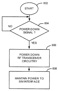
FIG. 6 is a flowchart for describing a method of controlling power to
electrical
circuitry of a wireless communication device having an interface for a smart
card (e.g. a
SIM card). These methods may be employed in components shown and described
above in relation to FIGs. 1-4. FIG. 6 relates to a method employed by a
wireless
communication device initially operating in a fully powered state (e.g. state
502 of FIG.
5). Beginning at a start block 602, the wireless device monitors its user
interface to
detect whether a (partial) power-off signal has been received (step 604). If
not received,
it continues monitoring the user interface. If the power-off signal is
detected as tested
in step 604, the wireless device (e.g. its microprocessor) powers OFF the RF
transceiver
circuitry of the wireless device (step 606). Even after detecting this power-
off signal,
however, the wireless device maintains power to the Subscriber Identity Module
(SIM)
interface (step 608).
Step 606 may be performed utilizing a regulator for the RF transceiver
circuitry
which is disabled or powered-off by the microprocessor in response to
detecting the
power-off signal (e.g. see FIG. 1 or FIG. 4). On the other hand, step 608 may
be
performed utilizing a regulator for the SIM interface (separate from the
regulator for the
RF transceiver circuitry) which is kept enabled or powered on by the
microprocessor
even after detecting the power-off signal (e.g. see FIG. 1 or FIG. 4). After
step 608, the
wireless device may be perceived as being in state 504 of FIG. 5 where it can
be used to
31
CA 02427369 2003-04-29
retrieve information stored on the SIM (e.g. address book information, SMS
messages,
PIM data, or any other suitable information) for display in the visual
display.
In this state, the wireless device may monitor its user interface to detect
whether
a power-on signal has been received. If the power-on signal is detected in
this state, the
wireless device (e.g. its microprocessor) powers ON the RF transceiver
circuitry while
maintaining power to the SIM interface. In alternate embodiment, the wireless
device
monitors its user interface to detect whether a power-on signal has been
received and, if
detected, prompts the end user (through the user interface, e.g. the visual
display) for a
password or PIN of the SIM. In response, the end user enters a password or PIN
and, if
it matches the stored password or PIN of the SIM, then the wireless device
(e.g. its
microprocessor) powers ON the RF transceiver circuitry while maintaining power
to
the SIM interface.
The above-described embodiments of invention are intended to be examples
only. Further alterations, modifications, and variations may be effected to
particular
embodiments by those of skill in art without departing from scope of
invention, which
is defined solely by claims appended hereto. For example, additional
regulators may be
utilized to separately regulate and/or control other portions of circuitry in
the wireless
device as desired. As another example, additional operational states or modes
of the
wireless device may be employed to further refine the operation of wireless
device as
desired.
32