Note: Descriptions are shown in the official language in which they were submitted.
CA 02427423 2003-04-30
WO 02/37686 PCT/US01/46188
METHOD AND APPARATUS FOR CONTROLLING
STAGES OF A MULTI-STAGE CIRCUIT
BACKGROUND OF THE INVENTION
I. Field of the Invention
The present invention relates to electronic circuits. More particularly,
the present invention relates to a novel and improved method and apparatus
for controlling stages of a multi-stage circuit such as a sigma-delta analog-
to-
digital converter (E0 ADC).
II. Description of the Related Art
An analog-to-digital converter (ADC) is an important component in
many electronic circuits, and is especially important in digital communication
systems. An ADC converts a continuous analog waveform into discrete
samples at evenly spaced time intervals. The samples can subsequently be
processed by other digital signal processing blocks to provide enhancement,
compression, and/or error detection/correction of the sampled data.
Exemplary applications which require ADCs are code division multiple access
(CDMA) communication system and high-definition television (HDTV).
Some important performance parameters of an ADC include linearity,
DC offset, and signal-to-noise ratio (SNR). Suboptimal values for these
parameters can cause degradation in the performance of a communication
system. Linearity relates to the difference between an actual transfer curve
(digital output versus analog input) and the ideal transfer curve. For a flash
ADC, good linearity is more difficult to obtain as the number of bits in the
ADC
increases. The DC offset can degrade the acquisition and tracking performance
of phase locked loops and the error detection/correction capability of the
decoder, such as the Viterbi decoder. SNR can affect the bit-error-rate (BER)
performance of the communication system because the quantization and circuit
noise from the ADC results in degradation of the sampled data.
In many communication systems, the received RF signal is
downconverted to baseband before quantization. Typically, the received signal
is downconverted from a RF frequency to an intermediate frequency (IF) in the
first downconversion stage. The first downconversion allows the receiver to
downconvert signals at various RF frequencies to a fixed IF frequency where
signal processing can be performed. For example, the fixed IF frequency allows
CA 02427423 2003-04-30
WO 02/37686 PCT/US01/46188
2
for a fixed bandpass filter, such as a surface acoustic wave (SAW) filter, to
remove undesirable images and spurious responses from the IF signal before
the second downconversion stage. The IF signal is then downconverted to
baseband where sampling is performed to provide the digitized baseband
samples.
In most communication applications, an ADC is required at the receiver.
In some applications, the receiver is a commercial unit where cost and
reliability are important design criteria because of the number of units
produced. Furthermore, in some applications, such as a CDMA mobile
communication system, power consumption is critical because of the
remote/portable nature of the receiver.
In the prior art, a flash ADC or a successive approximation ADC is used
to sample the received signal. In the flash ADC, the input signal is compared
against L-1 reference voltages, which are generated by a resistive ladder, by
L-1
comparators. Flash ADCs are bulky and consume large amount of power
because L-1 comparators and L resistors are required. Furthermore, flash ADCs
can have poor linearity and poor DC offset characteristics, if the L resistors
in
the resistive ladder are not matched. However, flash ADCs are popular
because of their high speed.
Successive approximation ADCs are also often used in communication
systems. These ADCs minimize complexity by performing approximations of
the input signal over two or more stages. However, these ADCs can also
exhibit the same poor linearity and poor DC offset characteristics as
exhibited
by the flash ADCs. Therefore, successive approximation ADCs as well as flash,
ADCs are not ideal candidates for use in many communication applications.
For some applications, improved data conversion performance can be
achieved with a sigma-delta ADC (E0 ADC).
SUMMARY OF THE INVENTION
The present invention provides a control mechanism that can be used to
control aEA ADC to provide the required level of performance while reducing
power consumption. The EO ADC is designed with multiple stages (i.e., loops
or sections), and provides improved performance (e.g., higher dynamic range)
as more stages are enabled. The control mechanism selectively enables a
sufficient number of stages to provide the required performance and disables
remaining stages to conserve power. The control mechanism achieves this by
measuring one or more characteristics (e.g., signal level) of the ADC input
signal through aE0 ADC that is similar to the ED ADC on the signal path,
CA 02427423 2003-04-30
WO 02/37686 PCT/US01/46188
3
comparing the measured characteristic(s) to particular threshold level(s), and
controlling the stages such that the desired objectives are achieved.
An embodiment of the invention provides a data conversion circuit that
includes aE0 ADC coupled to a control circuit. The E0 ADC includes a number
of EO stages coupled in cascade that receives an input signal and provides
data
samples. The control circuit includes one or more detector stages, a
conditioning circuit, and a signal processor. The detector stage(s) receive
the
input signal and provide a detected signal. The conditioning circuit couples
to
the detector stage(s), receives the detected signal, and provides conditioned
samples. The signal processor couples to the conditioning circuit, receives
the
conditioned samples, and provides a control signal that selectively disables
zero
or more EO stages.
In an embodiment, at least one detector stage is implemented as a replica
of one of the ED stages, and can be shrunken and/or biased with less current
than the ED stage it replicates. The detected signal can be indicative of an
amplitude of the input signal. The Y-A stages can be disabled based on the
detected signal amplitude, and possibly based on the relative locations of the
E0 stages within the Z0 ADC. In a specific implementation, the EA ADC
includes two fourth-order bandpass stages or two second-order lowpass stages.
The data conversion circuit is advantageously used in a cellular (e.g., CDMA)
receiver.
Another embodiment of the invention provides an electronic circuit that
includes a multi-stage circuit coupled to a control circuit. The multi-stage
circuit includes N signal stages coupled in a particular configuration (e.g.,
cascade, parallel, and others). The control circuit provides a control signal
that
selectively disables zero or more signal stages. The control circuit includes
one
or more detector stages, a conditioning circuit, and a signal processor that
can
be configured and operated as described above. The detector stage(s) can be
implemented as replica(s) of the signal stage(s), and can be shrunken and/or
biased with less current. The signal stages can be selectively disabled based
on,
for example, the amplitude of the input signal.
Yet another embodiment of the invention provides a control circuit for
controlling a multi-stage circuit that includes a number of signal stages. The
control circuit includes one or more detector stages, a conditioning circuit,
and
a signal processor. At least one detector stage is implemented as a replica of
one of the signal stages. The detector stage(s), conditioning circuit, and
signal
processor can be configured and operated as described above. The control
circuit is advantageously used to control aE0 ADC.
CA 02427423 2003-04-30
WO 02/37686 PCT/US01/46188
4
Yet another embodiment of the invention provides a method for
controlling EA stages in a EO ADC. In accordance with the method, a
characteristic of an ADC input signal is detected using one or more detector
stages. At least one detector stage is implemented as a replica of one of the
A.
stages. The detected characteristic is compared against a comparison level. A
control signal is generated based, in part, on the comparison. Zero or more EO
stages are then selectively disabled in accordance with the control signal.
The
characteristic being detected can be an amplitude of the input signal, and the
EO
stages can be disabled based on the detected signal amplitude.
BRIEF DESCRIPTION OF THE DRAWINGS
The features, nature, and advantages of the present invention will
become more apparent from the detailed description set forth below when
taken in conjunction with the drawings in which like reference characters
identify correspondingly throughout and wherein:
FIG. 1 is a block diagram of an exemplary single-loop sigma-delta
analog-to-digital converter (ED ADC) architecture; _
FIG. 2 is a block diagram of an exemplary MASH ED ADC architecture;
FIGS. 3A-3D are pole-zero diagram and frequency response plot of an
integrator and pole-zero diagram and frequency response plot of a bandpass
resonator, respectively;
FIG. 4 is a block diagram of an exemplary two loop bandpass MASH E0
ADC of the present invention;
FIGS. 5A-5E are block diagrams of a resonator within the bandpass
MASH EO ADC and implementations of the resonator with a delay cell
resonator, a lossless discrete integrator resonator, a Forward-Euler
resonator,
and a two-path interleaved resonator, respectively;
FIGS. 6A-6B are schematic diagram of a delay cell using double-
sampling switched capacitor analog circuit technique and timing diagram of the
required clock signals for the delay cell, respectively;
FIGS. 7A-7B are schematic diagrams of a resonator circuit within the
bandpass MASH EO ADC and the feed-forward gain circuit, respectively, both
of which are implemented using double-sampling switched capacitor analog
circuit technique;
FIG. 8 is a block diagram of an exemplary eighth order bandpass MASH
4-4 EO ADC of the present invention;
FIG. 9 is a plot of the simulated signal-to-noise ratio (SNR) performance
of the bandpass MASH 4-4 EO ADC of the present invention;
CA 02427423 2003-04-30
WO 02/37686 PCT/US01/46188
FIGS. 10A-10B are exemplary schematic diagrams of a delay cell based
resonator and a Forward-Euler resonator, respectively, both implemented using
single-sampling switched capacitor analog circuit technique;
FIGS. 10C-10D are exemplary schematic diagrams of a two-path
5 interleaved resonator implemented using pseudo two-path single-sampling
switched capacitor analog circuit and the timing diagram of the required clock
signals for the pseudo two-path circuit, respectively;
FIGS. 10E-10F are exemplary schematic diagrams of a two-path
interleaved resonator implemented using two independent path double-
sampling switched capacitor analog circuits;
FIGS. 10G-10H are exemplary schematic diagrams of a double-sampled
delay cell based resonator circuit and timing diagram of the required clock
signals for the resonator circuit, respectively;
FIGS. 11 through 13 show simplified block diagrams of three specific
embodiments of a control circuit for controlling a multi-stage circuit, which
can
be aE0 ADC as shown in Fig. 11;
FIG. 14 shows a simplified block diagram of a specific embodiment of a
control circuit that can be used as the control circuits in FIGS. 11 through
13;
FIG. 15A shows a graph of the standard deviation of the detected signal
from a detector stage versus input signal amplitude;
FIG. 15B shows a graph of the distribution densities of the signal levels
of the detected signal; and
FIG. 15C shows a graph of the count value from a signal processor
versus detector input signal amplitude.
DETAILED DESCRIPTION OF THE SPECIFIC EMBODIMENTS
A high-speed sigma-delta analog-to-digital converter (EO ADC)
performs analog-to-digital conversion of the input signal by making successive
one-bit approximations of the change in amplitude of the input signal, since
the
previous sample has already been approximated, at a sampling rate which is
many times higher than the bandwidth of the input signal. The output samples
comprise the input signal and the quantization noise. The ED ADC can be
designed such that the quantization noise is pushed (or noise shaped) to an
out-
of-band frequency where filtering is more easily performed.
A EO ADC can provide high signal-to-noise ratio (SNR), good linearity,
and low DC offset because of the inherent structure of EA ADC. For example,
high SNR can be obtained by selecting a sufficient oversampling ratio (OSR)
CA 02427423 2003-04-30
WO 02/37686 PCT/US01/46188
6
and the appropriate noise shaping filters. Additionally, good linearity and
low
DC offset are obtained because of the simple one-bit quantizer within the E
ADC.
High-speed bandpass EA ADC can be used to perform the required
analog-to-digital conversion of narrowband signals at an intermediate
frequency (IF). Exemplary applications include CDMA communication system
and HDTV. In a bandpass EA ADC, the input signal is at an IF frequency
instead of baseband. Sampling at IF allows for the elimination of a
downconversion stage in the communication system, thus reducing circuit
complexity, decreasing cost, and improving reliability. Furthermore, the noise
shaping filters within the bandpass ED ADC can be designed such that the
quantization noise around the band of interest is pushed to out-of-band
frequencies where filtering is more easily performed.
EA ADC samples an analog waveform in continuous time to provide
discrete samples at evenly spaced time intervals. EA ADC has the following
transfer function :
Y(z) = G(z)' X(z) + H(z)' E(z) ~ (1)
where Y(z) is the output from the EO ADC in the z-transform domain, X(z) is
the input to the ADC, E(z) is the quantization noise, G(z) is the transfer
function
from the input to the output, and H(z) is the noise transfer function from the
quantizer to the output. Thus, the ADC output Y(z) comprises the input signal
X(z) that is shaped by the transfer function G(z) plus the quantization noise
E(z)
which is shaped by the noise transfer function H(z). To avoid distortion of
the
input signal X(z), the transfer function G(z) is typically designed such that
it is
frequency independent. For example, G(z) can be an allpass function
comprising a fixed gain (A1) and delay elements (z 1), such as A2 =z m. The
quantization noise E(z) can be shaped by the noise transfer function H(z) such
that the quantization noise in the band of interest (e.g. the band where the
input
signal is present) is pushed out-of-band where filtering is more easily
performed. The characteristics of the noise transfer function H(z) is selected
based on the application for which the Y-0 ADC is used and is designed to
provide the required performance.
CA 02427423 2009-03-17
74769-661
7
I. EA ADC Architectures
EA ADC can be designed using one of many architectures. A block
diagram of an exemplary single-loop EA ADC 10 is shown in FIG. 1. Single-
loop EA ADC 10 comprises input summer 22 that subtracts the quantized ADC
output from the ADC input. The error signal from summer 22 is provided to
first filter 24 that filters the error signal in accordance with the transfer
function
of first filter 24. The output of first filter 24 is provided to summer 26
that
subtracts the quantized ADC output from the output of first filter 24. The
error
signal from summer 26 is provided to second filter 28 that filters the error
signal
in accordance with the transfer function of second filter 28. The output of
second filter 28 is quantized, typically to one bit although more bits can
also be
used, and provided as the quantized ADC output.
FIG. 1 illustrates a single loop EA ADC with two filter sections. The filter
sections determine the noise shaping characteristics of the EA ADC and is
designed based on the application for which the EO ADC is used. More filter
sections can be interposed between second filter 28 and quantizer 30. However,
single-loop EA ADCs are typically designed with two or less filter sections
because of concerns with instability of higher order single-loop EA ADCs.
A block diagram of an exemplary MASH EO ADC architecture is shown
in FIG. 2. A MASH ADC can be designed with two or more loops, depending
on the desired noise transfer function H(z). However, MASH ADCs with more
than three loops are not typically utilized because small incremental
improvement is achieved for additional loops greater than three. The MASH
architecture is preferred for a higher order EA ADC since the MASH
architecture is inherently stable.
As shown in FIG. 2, a MASH ADC 12 comprises three loops 40a, 40b,
and 40c. Loop 40a quantizes the ADC input and provides the output Yl to
noise cancellation logic 90. The operation of noise cancellation 90 is
described
in detail below. A fraction of the ADC input and quantization noise (X2) from
loop 40a is provided to loop 40b where additional noise shaping is performed.
Finally, a fraction of the ADC input and quantization noise (X3) from loop 40b
is provided to loop 40c where further noise shaping is performed. The output
Y2 from loop 40b and Y3 from loop 40c are provided to noise cancellation logic
90 where they are combined with the output Yl from loop 40a to produce the
ADC output. In the exemplary embodiment, ADC output comprises one bit for
CA 02427423 2003-04-30
WO 02/37686 PCT/US01/46188
8
each loop. After noise cancellation, the dynamic range, and thus the output of
MASH ADC 12, can be three bits or more.
Within each loop 40, summer 42 receives the input signal and the
quantizer output from quantizer 46. Summer 42 subtracts the quantizer output
from the input signal and provides the error signal to loop filter 44. Loop
filter
44 filters the error signal and provides the filtered output to quantizer 46
where
it is quantized to one-bit values. Loop filter 44 is designed to produce the
desired noise transfer function H(z) that is based on the application for
which
the EA ADC is used. The filtered output from loop filter 44 in all but the
last
loop 40c is provided to gain element 52 and scaled with a first gain. The
output
from quantizer 46 in all but the last loop 40c is provided to gain element 54
and
scaled with a second gain. The scaled signal from gain element 54 is
subtracted
from the scaled signal from gain element 52 by summer 56 and the error signal
is provided to gain element 56. Gain element 56 scales the error signal with a
third gain and provides the scaled error signal to the subsequent loop 40. The
gains of gain elements 52, 54, and 58 affect the noise transfer function H(z)
of
MASH ADC 12.
Each loop filter 44 can comprise one or more filter sections, depending
on the desired noise transfer function. More filter sections allow for
implementation of higher order EA ADC to produce the desired performance,
such as high SNR. A loop filter design is described in detail below.
In this specification, a MASH EA ADC is designated in accordance with
the following nomenclature. MASH A-B-C denotes three loops (A, B, and C)
which are of the order designated by the values of A, B, and C. For example,
MASH 4-2-2 denotes a three loop architecture, with the first loop having a
fourth order filter, the second loop having a second order filter, and the
third
loop also having a second order filter. Overall, MASH 4-2-2 is an eighth order
Eb ADC. The present invention can be directed toward a MASH 2-2, MASH 4-
2, MASH 4-4, MASH 4-2-2, MASH 4-4-2, MASH 4-4-4 and other orders of
MASH EA ADC.
The selection of the desired E0 ADC architecture, single-loop or MASH,
depends on a number of factors. One important factor is the required signal-to-
noise ratio (SNR). SNR is defined as the ratio of the power of the largest
input
signal to the power of the quantization noise. For a full-scale sinewave
input,
the SNR for aE0 ADC can be calculated according to the following equation :
ISNR = 3, 2~ L 1=(OSR~a z+i . (2)
CA 02427423 2003-04-30
WO 02/37686 PCT/US01/46188
9
where L is the order of the loop filter used for noise shaping and OSR is the
oversampling ratio. OSR is defined as the ratio of the sampling rate over the
OSR = f
two-sided signal bandwidth, 2f$W . Equation (2) is based on the simple
theory using only white quantization noise and a unity gain quantizer.
Using equation (2) the SNR is calculated for an exemplary CDMA application
wherein the 2-sided signal bandwidth 2fByV = 2.4576 MHz and the sampling
rate is approximately 78.64 MHz. These frequencies produce an OSR of 32. The
SNR is calculated for various loop filter order L and the results are
tabulated in
Table 1. The loop filter order is the summation of the order of all filters
within
the EO ADC. For a bandpass ED ADC, the loop filter order L is half of the
overall order of the bandpass filters. An n-th order bandpass filter has an
effective order of L = n/2 because the poles in the bandpass transfer function
are divided evenly between the upper half of the z-plane and the lower half of
the z-plane. The calculated SNR values in Table 1 represent the upper bound
that can be achieved. The actual SNR may be 10 dB to 15 dB less than the
calculated values due to non-ideal circuit components and limitation of the
input signal to less than the full-scale value.
For the CDMA application described above, the SNR is simulated to be 70 dB
for a bandpass MASH 4-2 ADC, 85 dB for a MASH 4-4, 60 dB for a sixth order
single-loop bandpass EA ADC, and 62 dB for an eighth order single-loop ADC.
The simulated results are also tabulated in Table 1. The simulated results
assume an input signal at -10 dB below full-scale and coincident zeros (e.g.
all
zeros are placed at z = j) in the noise transfer function H(z). The simulated
SNR value for the sixth order single-loop EA ADC can be improved to 70 dB if
the zeros are spread across the signal bandwidth. Similarly, the simulated SNR
value for the eighth order single-loop ED ADC can be improved to 80 dB with
zero spreading. However, zero spreading can be difficult to achieve due to
non-ideal circuit components. The simulated SNR of a MASH architecture is
better than that of the single-loop architecture.
CA 02427423 2003-04-30
WO 02/37686 PCT/US01/46188
Table 1- Calculated and Simulated SNR for EO ADC of Various Order
SNR (dB)
loop order BPF order calculated simulated simulated simulated
L MASH 4-2 MASH 4-4 sin le-loo
2 4 64
3 6 85 70 60
4 8 107 85 62
In actual implementation, the MASH architecture has the additional
advantages of inherent stability and ease of loop filter design. However,
circuit
5 matching is more critical for the MASH architecture because of the need to
cancel the quantization noise between multiple loops. The single-loop
architecture is stable for second order or lower order loops but may be
unstable
for higher order loops. Higher order single-loop designs can be made stable by
careful circuit design and thorough simulation. However, the single-loop
10 architecture is more tolerant to circuit mismatch. The selection of the
single-
loop or MASH architecture is dependent on the requirements of the application.
For most applications, the MASH architecture is preferred over the single-loop
architecture.
The noise transfer function H(z) of MASH ADC 12 is determined by the
design of loop filters 44. For example, a baseband MASH E0 ADC can be
designed by implementing loop filters 44 with lowpass filters. Similarly, a
bandpass EA ADC can be designed by implementing loop filters 44 with
bandpass filters. The noise transfer function H(z) of the quantization noise
is
the inverse of the filter characteristics because the loop filters reside
within the
loops.
An exemplary baseband MASH E0 ADC can be designed by
implementing loop filters 44 with one or more integrators having the lowpass
z-i
transfer function 1-z-1 . The number of integrators within loop filters 44
depends on the desired noise transfer function H(z). As shown in FIG. 3A, the
lowpass transfer function has a pole at z = +1 and a zero at the origin z = 0.
The
frequency response of the lowpass transfer function is shown in FIG. 3B by the
solid line. The lowpass filter has the highest gain at DC because of the pole
at
z = +1, a gain of 1.0 at fs/6, and a gain of 0.5 at fs/2 where fs is the
sampling
frequency. The frequency response of the noise transfer function is shown in
CA 02427423 2003-04-30
WO 02/37686 PCT/US01/46188
11
FIG. 3B by the dashed line. The quantization noise around DC is pushed
toward higher frequency.
An exemplary bandpass MASH EO ADC can be designed by
implementing loop filters 44 with one or more resonators having the bandpass
_Z z
transfer function i+z-2. The number of resonators within loop filters 44
depends on the desired noise transfer function H(z). For example, a fourth
order loop requires two resonator sections each having the bandpass transfer
function as described above. A bandpass transfer function can be obtained
from a lowpass transfer function by substituting z 1 in the lowpass transfer
function with -z -2. As shown in FIG. 3C, the bandpass transfer function has a
pair of poles at z = j and two zeros at the origin z = 0. The frequency
response
of the bandpass transfer function is shown in FIG. 3D by the solid line. The
bandpass filter has the highest gain at fs/4, because of the poles at z = j,
and a
gain of 0.5 at DC and at fs/2. The frequency response of the noise transfer
function is shown in FIG. 3D by the dashed line. The quantization noise around
fs/4 is pushed away from fs/4, the frequency band of interest, toward DC and
fs/2.
II. Bandpass MASH EO ADC Architecture
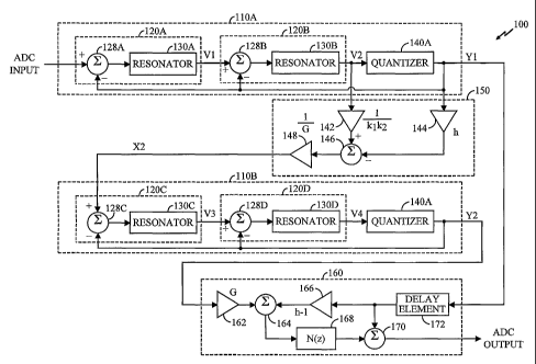
A block diagram of an exemplary two loop bandpass MASH E0 ADC is
illustrated in FIG. 4. MASH ADC 100 comprises two loops 110a and 110b, feed
forward element 150, and noise cancellation logic 160. In the exemplary
embodiment, MASH ADC 100 receives an analog ADC input and produces a
digital ADC output having at least two bits, at least one bit for each loop
110.
The ADC input is provided to loop 110a that produces a 1-bit output Yl
in response thereto. A fraction of the ADC input and quantization noise (X2)
from loop 110a is provided to loop 110b where additional noise shaping is
performed. The outputs Yl and Y2 from loops 110a and 110b, respectively, are
provided to noise cancellation logic 160. Noise cancellation logic 160
combines
the outputs Yl and Y2 and produces the ADC output.
Within loop 110a, summer 128a receives the ADC input and the 1-bit
output Yl from quantizer 140a. Summer 128a subtracts Yl from the ADC input
and provides the error signal to resonator 130a. Resonator 130a filters the
error
signal and provides the filtered output (V1) to summer 128b. Summer 128b
also receives Yl from quantizer 140a and subtracts Yl from V1. The error
signal
from summer 128b is provided to resonator 130b that further filters the error
CA 02427423 2003-04-30
WO 02/37686 PCT/US01/46188
12
signal. The filtered output (V2) from resonator 130b is provided to quantizer
140a that produces the 1-bit output Yl in response thereto. Loop 110b is
connected in similar manner as loop 110a.
The filtered output V2 from resonator 130b is also provided to gain
element 142 which scales V2 by the scaling factor 1/kjk2. The output Yl from
quantizer 140a is provided to gain element 144 that scales Yl by the scaling
factor h. The outputs from gain elements 142 and 144 are provided to summer
146 which subtracts the output from gain element 144 from the output from
gain element 142. The error signal from summer 146 is provided to gain
element 148 that scales the error signal by the scaling factor 1/G. The output
from gain element 148 comprises X2 that is provided to loop 110b.
Within noise cancellation logic 160, the output Yl is provided to delay
element 172 which delays Y1 by a time interval equal to the processing delay
of
loop 110b. The delayed Yl from delay element 172 is time aligned with Y2.
The output Y2 is provided to gain element 162 which scales Y2 by the scaling
factor G. The delayed output Yl is provided to gain element 166 that scales
the
delayed Yl by the scaling factor h-1. The outputs from gain elements 162 and
166 are provided to summer 164 that sums the two scaled outputs. The
combined signal from summer 164 is provided to element 168 that filters the
combined signal with the transfer function N(z). The output from element 168
and the delayed Yl are provided to summer 170 which sums the two signals to
produce the ADC output.
For a bandpass EA ADC, each resonator 130 in MASH ADC 100 is
/C.7.n, z-Ill
implemented with a bandpass transfer function 1 + z 2, where kn is the gain of
the n-th resonator 130 within loop 110 and m = 1 or 2. Each resonator 130
comprises a pair of poles and is second order. Since each loop 110 contains
two
resonators 130, the order of each loop is four. Overall, MASH ADC 100 is an
eighth order MASH 4-4 ADC. The transfer function N(z) within element 168 is
selected based on the characteristics of the EA ADC. For a bandpass EA ADC,
2 2
N(z) =~1 +Z ~. Delay element 172 has a transfer function of z-2m .
The gains k1, k2, h, and G which are reflected in the scaling factors of
gain elements 142, 144, 148, 162, and 166 determine the location of the zeros
of
the noise transfer function H(z). The poles in resonators 130 are transformed
into zeros in the noise transfer function H(z) because the resonators reside
within a feedback loop. Initially, the zeros in H(z) are selected to be at z =
j for
the bandpass EA ADC.
CA 02427423 2003-04-30
WO 02/37686 PCT/US01/46188
13
MASH ADC 100, as illustrated in FIG. 4, is a bandpass EA ADC. The
same topology can be used to implement a baseband EO ADC. This can be
easily achieved by substituting each resonator 130 with an integrator having
the
z-i
lowpass transfer function 1- z implementing element 168 with the transfer
1 Z
function N(z) zand providing delay element 172 with the transfer
function z-2. With these substitutions, MASH ADC 100 is transformed into a
fourth order baseband MASH 2-2 ADC.
In the exemplary embodiment, all elements of MASH ADC 100, except
for noise cancellation logic 160, are implemented as analog circuits. However,
the optimal implementation of an element in either analog or digital circuit
may
depend on the IC process used in implementing the EA ADC. Therefore, the
various combinations of analog and digital circuits to synthesize the required
elements within MASH ADC 100 are within the scope of the present invention.
III. Bandpass Resonator Design
A bandpass MASH 4-4 ADC can be designed by implementing
Z-z
resonators 130 in MASH ADC 100 with a bandpass transfer function 1+ z 2 as
described above. Thus, resonators 130a, 130b, 130c, and 130d have the same
structure. However, the gain of resonators 130a and 130c is kl whereas the
gain
of resonators 130b and 130d is k2. Resonator 130 is illustrated in FIG. 5A.
Resonator 130 can be implemented by many resonator structures, four of which
are illustrated in FIGS. 5B-5E. Resonators 131, 132, 133 and 134 receive the
input signal Rin and produce the output signal Rout.
A block diagram of an exemplary delay cell resonator 131 is shown in
FIG. 5B. The input signal Rin is provided to gain element 192 that scales the
input signal with the gain kn. The scaled Rin is provided to summer 194 that
also receives the output signal Rout and subtracts Rout from the scaled Rin.
The error signal from summer 194 is provided to delay element 200a that delays
the signal by one clock cycle of the sampling clock. The delayed error signal
from delay element 200a is provided to delay element 200b which further
delays the signal by one sampling clock cycle. The signal from delay element
200b comprises the output signal Rout.
A block diagram of an exemplary lossless discrete integrator (LDI)
resonator 132 is shown in FIG. 5C. The input signal Rin is provided to gain
CA 02427423 2003-04-30
WO 02/37686 PCT/US01/46188
14
element 260 that scales the input signal with the gain kn. The scaled Rin is
provided to summer 262 that also receives the scaled output signal Rout and
subtracts the scaled Rout from the scaled Rin. The error signal from summer
262 is provided to filter 264 which filters the signal with the transfer
function
z-1
1-z . The filtered error signal from filter 264 is provided to filter 266 that
1
further filters the signal with the transfer function 1- z-1 . The signal from
filter
266 comprises the output signal Rout. Rout is provided to gain element 268
that scales Rout with the gain (3. In the exemplary embodiment, (3 = 2 and the
kn' z 1
overall transfer function of resonator 132 is 1+z-2 . By proper selection of
(3,
the zeros of the noise transfer function can be spread in the signal band.
A block diagram of an exemplary Forward-Euler (FE) resonator 133 is
shown in FIG. 5D. The input signal Rin is provided to gain element 270 that
scales the input signal with the gain kn. The scaled Rin is provided to summer
272a that also receives the scaled output signal Rout and subtracts the scaled
output signal Rout from the scaled input signal Rin. The error signal from
summer 272a is provided to filter 274a that filters the signal with the
transfer
~
z -2
k,
function 1+ z 2. The filtered error signal from filter 274a is provided to
summer
272b that also receives the scaled Rout and subtracts the scaled Rout from the
filtered error signal. The error signal from summer 272b is provided to filter
k,, . z-2
274b that filters the signal with the transfer function 1+ z-Z . The signal
from
filter 274b comprises the output signal Rout. Rout is provided to gain element
276 that scales the output signal Rout with the gain P. In the exemplary
kn,z 2
embodiment, (3 = 2 and the overall transfer function of resonator 133 is 1 + z
Z
A block diagram of an exemplary two-path interleaved resonator 134 is
shown in FIG. 5E. The input signal Rin is provided to gain element 280 that
scales the input signal with the gain kn. The scaled Rin is provided to
switches
282a and 282b which connects the scaled Rin to summers 284a and 284b,
respectively. Summer 284 also receives the delayed error signal from delay
elements 286 and subtracts the delayed error signal from the scaled Rin. The
error signal from summer 284 is provided to delay element 286 which delays
the error signal by one sampling clock cycle. The delayed error signal from
delay elements 286a and 286b are provided to switches 288a and 288b,
respectively. Switches 288a and 288b connect together and comprise the output
CA 02427423 2003-04-30
WO 02/37686 PCT/US01/46188
of resonator 134. Switches 282a and 288a are clocked by one phase of a
switching clock and switches 282b and 288b are clocked by a second phase of
the switching clock. The clock signals are described in detail below. The
kn, z 2
overall transfer function of resonator 134 is 1+ z 2
5 Resonators 131, 132, 133 and 134 can be implemented by numerous
analog circuit techniques. For example, resonators 131, 132, 133 and 134 can
be
implemented with continuous time analog circuit techniques such as active-RC,
gm-C, and MOSFET-C. Resonators 131, 132, 133 and 134 can also be
implemented with sampled-data analog circuit techniques such as switched
10 capacitor and switched current. The selection of the analog circuit
technique
depends on the requirement of the application for which the E0 ADC is used.
For an exemplary CDMA application wherein a 12-bit EO ADC operating at a
sampling rate of 80 MHz, the performance of the various circuit techniques is
tabulated in Table 2.
Table 2- Performance of Various Analog Circuit Techniques
analog circuit resolution accuracy speed technology
technique SNR (time constant)
active-RC yes no yes bipolar J
CMOS
gm-C possibly yes yes BiCMOS
(with tuning)
switched yes yes yes CMOS
capacitor
switched current possibly yes yes digital
CMOS
The implementation of the functions as described herein using any one
of the circuit techniques listed in Table 2, or its equivalents, are within
the scope
of the present invention. In the preferred embodiment, resonators 131, 132,
133
and 134 are implemented with a switched capacitor circuit technique because of
superior performance in SNR, accuracy, speed, and cost.
The design of resonator 131 using the switched capacitor circuit
technique is described in detail below. Within resonator 131, each delay
element 200 can be implemented by one of many analog circuit techniques. In
the preferred embodiment, delay element 200 is implemented with a double-
CA 02427423 2003-04-30
WO 02/37686 PCT/US01/46188
16
sampling switched capacitor delay circuit 210 as illustrated in FIG. 6A. For
optimal linearity and noise performance, delay circuit 210 is implemented as a
fully differential circuit, where the input comprises Rin+ and Rin- and the
output comprises Rout+ and Rout-.
Within delay circuit 210, the input signal Rin+ is provided to two signal
paths through switches 220a and 224a. Switch 220a connects to one end of
capacitor 228a and switch 236a. The other end of capacitor 228a connects to
switches 222a and 232a. Switch 222a also connects to AC ground 202. Switch
232a also connects to the inverting input of amplifier 250 and switch 236a
also
connects to the non-inverting output of amplifier 250. In similar manner,
switch 224a connects to one end of capacitor 230a and switch 238a. The other
end of capacitor 230a connects to switches 226a and 234a. Switch 226a also
connects to AC ground 202. Switch 234a also connects to the inverting input of
amplifier 250 and switch 238a also connects to the non-inverting output of
amplifier 250. Delay circuit 210 is a fully differential circuit. The lower
half of
delay circuit 210 is a mirror image of the upper half.
AC ground 202 is implemented as a DC bias voltage with a capacitor
bypass to ground. The DC bias voltage determines the mid-scale voltage of the
differential signal at that node. For best linearity, the signals Rin+ and Rin-
are
normally biased near the operating center of amplifier 250. In some circuit
design, the differential output Rout+ and Rout- can have a different optimal
DC
bias voltage than that of the input Rin.
Delay circuit 210 samples the input signal Rin on two phases of the
switching clock. Referring to FIG. 6B, the sampling clock fs is divided by two
to
obtain the switching clock. In the exemplary embodiment, the clock signal
CLK1 having the first clock phase ol is provided to the switches which are
shown without the bubble (e.g. switch 224a). The clock signal CLK2 having the
second clock phase o2 is provided to the switches which are shown with the
bubble (e.g. switch 220a). Each clock signal should have a duty cycle that is
less
than 50 percent. The minimum width of the clock signals is determined by the
charging time of the capacitors which, in turn, is determined by the size of
the
capacitor and the ON resistance of the switches.
Referring to FIG. 6A, during the first clock phase ol, switches 224a and
226a are switched ON and capacitor 230a is charged with the input signal Rin+.
During the second clock phase o2, switches 224a and 226a are switched OFF,
switches 234a and 238a are switched ON, and the voltage across capacitor 230a
is provided to the output Rout+. Capacitor 230a is charged during the first
clock phase ol and provided to the output Rout+ during the second clock phase
CA 02427423 2003-04-30
WO 02/37686 PCT/US01/46188
17
o2. Therefore, the delay provided by delay circuit 210 is a half switching
clock
cycle, or one sampling clock cycle. Similarly, capacitor 228a is charged
during
the second clock phase o2 and provided to the output Rout+ during the first
clock phase ol. The two signal paths, one through capacitor 230a and the
second through capacitor 228a, operate on different clock phases and only
share
amplifier 250.
Using double-sampling switched capacitor circuit, the input signal Rin is
provided to the output Rout on both phases of the switching clock, through two
signal paths, thereby resulting in the sampling of Rin at the sampling clock
frequency fs even though the switches are switched ON and OFF at half the
sampling clock (fs/2). A double-sampling switched capacitor circuit allows the
switches to be clocked at half the sampling frequency, thus allowing the
capacitors and amplifier more time to settle to the final value. Since the
operating speed of a switched capacitor circuit is determined by the settling
time of the amplifier used in the circuit, using the same amplifier during
both
phases of the switching clock increases the sampling rate by a factor of two
without requiring faster settling amplifier.
However, double-sampling switched capacitor circuits are sensitive to
path mismatch. Mismatch in the first sampling stage of the ED ADC can cause
degradation in the output samples. Mismatch in the subsequent stages is noise
shaped and does not result in noticeable degradation. Any mismatch between
the two signal paths, such as mismatch in the capacitors or mismatch due to
uneven clock phases, in the first stage produces an image of the input signal
to
appear at the output samples. By using good circuit design rules, the
capacitor
mismatch can be reduced to one percent or less, thereby minimizing the
amplitude of the image to -40 dB or more below the amplitude of the input
signal. The switching clocks can be designed to minimize uneven clock phases.
Alternatively, the first sampling stage can be clocked with a master clock,
before the divide-by-two operation to obtain the switching clocks. Clock
jitter
can be reduced by using a clean external clock source. This topology also have
faster settling time than the single-sampled topology because of less
amplifier
loading.
IV. Bandpass MASH 4-4 ADC Design
Referring to FIG. 4, each loop 110 comprises two resonator sections 120.
Each resonator section 120 comprises summer 128 and resonator 130.
Resonator 130 can be implemented as delay cell resonator 131 as shown in FIG.
CA 02427423 2003-04-30
WO 02/37686 PCT/US01/46188
18
5B. Each delay cell resonator 131 comprises two delay elements 200. Each
delay element 200 can be implemented with double-sampling switched
capacitor delay circuit 210 as shown in FIG. 6A.
A schematic diagram of double-sampling switched capacitor resonator
circuit 121, which implements resonator section 120, is shown in FIG. 7A.
Resonator circuit 121 comprises delay element and summer circuit 300 and
delay circuit 310. Circuit 300 incorporates summer 128, gain element 192,
summer 194, and delay element 200a (see FIGS. 4 and 5B). Delay circuit 310
implements delay element 200b.
Referring to FIG. 7A, within circuit 300, the input signal Vip is provided
to two signal paths, the first signal path through switch 324a. Switch 324a
connects to one end of capacitor 330a and switch 314a. The other end of
capacitor 330a connects to switches 326a and 334a. Switch 326a also connects
to
AC ground 202 and switch 334a also connects to the inverting input of
amplifier
350a. Switch 314a connects to the quantizer output Ypra1 that is described
below. Switches 326a and 334a connect to one end of capacitor 318a. The other
end of capacitor 318a connects to switches 344a and 338a. Switch 338a also
connects to the non-inverting output of amplifier 350a. Switch 344a also
connects to the inverting output of amplifier 350b within delay circuit 310.
The operation of the first signal path in circuit 300 can be described as
follows. During the first clock phase o1, switches 324a and 326a are switched
ON and capacitor 330a is charged with the input signal Vip. During the second
clock phase e2, switches 324a and 326a are switched OFF and switches 314a,
334a, and 338a are switched ON. The input signal Yxpol and the voltage across
capacitor 330a are scaled by the ratio of capacitors 330a and 318a (Cs/Cf) and
provided to the non-inverting output of amplifier 350a. Also during the first
clock phase ol, switch 344a is switched ON and the signal from the inverting
output of amplifier 350b is fed back, charging capacitor 318a. The voltage
across capacitor 318a is reflected at the non-inverting output of amplifier
350a
during the second clock phase o2.
The above discussion describes the circuit connection and operation of
the first signal path within circuit 300. An identical circuit is provided for
the
second signal path which operates in the same manner as that of the first
signal
path, except the switches are clocked at the alternative phase of the
switching
clock. Thus, the input signal Vip is provided to the output of amplifier 350a
on
both phases of the switching clock and results in the sampling of the input
signal at the sampling rate.
CA 02427423 2003-04-30
WO 02/37686 PCT/US01/46188
19
Circuit 300 is a fully differential circuit. An identical circuit is provided
for the inverting input signal Vin. The lower half of circuit 300 is the
mirror
image of the upper half.
Circuit 300 includes the functions of summer 128, gain element 192, and
summer 194 (see FIGS. 4 and 5B). The function of summer 194 is provided by
switches 342 and 344 which connects the output of the second delay element to
capacitors 316 and 318, respectively. The voltage Von is stored in capacitor
318a during the first clock phase o1 and subtracted from the voltage at Vb
during the second clock phase e2. The function of summer 128 is provided by
switches 312 and 314 that connect the quantizer output to capacitors 328 and
330, respectively. The quantizer output voltage Ypol is provided to capacitor
330a during the second clock phase o2 and is added to the voltage at Vb.
Delay circuit 310 is identical to delay circuit 210 in FIG. 6A and operates
in the same manner as that described above for delay circuit 210. Delay
circuit
310 delays the output from circuit 300 by a half switching clock cycle, or one
sampling clock cycle. The output from amplifier 350b comprises the output of
resonator circuit 121.
Resonator circuit 121 has the following transfer function from Vip to Vop
C r z z
HR(Z a
) Cf 0 l+ z z ' (3)
The transfer function from Yxpol to Vop is -HR(z). In this nomenclature, Yx
denotes the quantizer output from the first (x = 1) or second (x = 2) loop, p
or n
denotes a (+) or (-) signal, and ral or o2 denotes the clock phase of the
quantizer
output. The voltage gain from Yxpol to Vop is -Cs/Cf, the ratio of capacitor
330a to capacitor 318a. Thus, the gain of gain element 192 can be set as
kn = Cs/Cf.
Having implemented each resonator section 120 with resonator circuit
121, MASH ADC 100 in FIG. 4 can be implemented as an eighth order bandpass
MASH 4-4 ADC 101 as shown in FIG. 8. Each resonator section 120 in FIG. 4 is
replaced with double-sampling switched capacitor resonator circuit 121 in FIG.
8. Within resonator circuit 121, the feedback from delay circuit 310 to
circuit
300 is not shown for simplicity. Also, note that noise cancellation logic 160
in
FIG. 4 is not shown in FIG. 8 for simplicity.
CA 02427423 2003-04-30
WO 02/37686 PCT/US01/46188
Quantizer 140a in FIG. 4 is implemented with quantizer 141a which
comprises two synchronous comparators 390a and 390b. Comparator 390a is
clocked by CLK1 having the first phase o1 and comparator 390b is clocked by
CLK2 having the second phase o2 (see FIG. 6B). The differential input signals
5 to comparators 390a and 390b are provided by the output of circuit 300b.
This
is because quantizer 141a has a delay of a half switching clock cycle. The
input
to quantizer 141a is taken before delay circuit 310b which also provides a
delay
of a half switching clock cycle. Connected in this manner, quantizer 141a is
properly aligned in time. Each comparator 390 provides a differential output.
10 Comparator 390a provides the differential output signals Ylpol and Y1nra1
and
comparator 390b provides the differential output signals Y1po2 and Y1no2.
The four quantizer outputs, collectively referred to as Yl, are provided to
circuits 300a, 300b, and 151 as shown by FIGS. 4 and 8.
Referring to FIGS. 4 and 8, feed forward gain element 150 can be
15 incorporated into circuit 300c to simplify the circuit design. Referring to
FIG. 4,
the gain from the output (V2) of resonator 130b to X2 is 1/k1k2G and the gain
from the output (Y1) of quantizer 140a to X2 is -h/G. The overall transfer
function of feed-forward gain element 150 can be calculated as X2 = Av1 = V2-
Av2=Y1, where Av1=1/k1k2G and Av2 = h/G.
20 The gains k1, k2, h, and G of bandpass MASH 4-4 ADC 101 are selected
for optimal SNR and ease of circuit implementation. Using mixed analog and
digital design simulation tools, the following exemplary values are selected
for
the gains :
1k1= 0.5, kZ = 0.5, lz = 2, G= 4. (4)
Other values for gains k1, k2, h, and G can also be utilized and are within
the
scope of the present invention. Using the gain values as shown in equation
(4), and an oversampling ratio of 32, the SNR versus input signal level is
plotted
in FIG. 9. The peak SNR surpasses 90 dB.
A schematic diagram of an exemplary feed-forward gain circuit 151,
which in conjunction with circuit 300c implements feed-forward gain element
150, is illustrated in FIG. 7B. The quantizer outputs Y1po2, Y1pg1, Y1no1, and
Ylno2 from quantizer 141a (see FIG. 8) are provided to switches 372a, 376a,
376b, and 372b, respectively. Switches 372a, 376a, 376b, and 372b connect to
one end of capacitors 380a, 382a, 382b, and 380b which are connected to node
Va, Vb, Vc, and Vd within resonator circuit 121 in FIG. 7A, respectively. The
CA 02427423 2003-04-30
WO 02/37686 PCT/US01/46188
21
other end of capacitors 380a, 382a, 382b, and 380b, connect to switches 374a
and
384a, 378a and 386a, 378b and 386b, and 374b and 384b, respectively. Switches
374a, 378a, 378b, 374b, 384a, 386a, 386b, and 384b also connect to AC ground
202.
The gain values Avl and Av2 can be calculated and incorporated into
feed forward gain circuit 151. Using the values of kl = 0.5, k2 = 0.5, h= 2,
and
G=4 from equation (4), the gain values become Av1=1.0 and Av2 = 0.5.
Referring to FIGS. 7A and 7B, the gain from the output Y1pra1 of quantizer
141a
to the non-inverting output of amplifier 350a is determined by the ratio of
capacitors 382a and 318a, or Av2 = Cq/Cf = 0.5. Therefore, the capacitance of
capacitor 382a is synthesized to be half of the value of capacitor 318a.
Referring
to FIG. 8, the gain from the output V2p of resonator circuit 121b
(corresponding
to Vip in FIG. 7A) to the non-inverting output of amplifier 350a is determined
by the ratio of capacitors 330a and 318a, or Av1= Cs/Cf =1Ø Thus, the value
of capacitor 330a is synthesized to be the same capacitance as capacitor 318a.
However, capacitors 330a and 318a also implement gain element 192 (see FIG.
5B). In the exemplary embodiment, the gains kn = k1= k2 = 0.5 as shown in
equation (4). Therefore, capacitor 330a is selected to be half the capacitance
of
capacitor 318a.
In the exemplary embodiment, noise cancellation circuit 160 in FIG. 4 is
implemented in digital logic. For an eighth order bandpass MASH EA ADC,
delay element 172 has a transfer function of z 4 and can be implemented with
four D flip-flops connected in cascade, the design and implementation of which
are known in the art. The transfer function of element 168 is N(z) _~1 + z z 2
~
which can be implemented with two summers and four sets of D flip-flops, the
implementation of which is also known in the art.
As stated above, double-sampling switched capacitor circuits are
sensitive to path mismatch. However, path mismatch in the stages subsequent
to the first sampling stage is noise shaped and does not cause a noticeable
image. Referring to FIG. 8, within delay element and summer circuit 300a,
which is illustrated in FIG. 7A, only the input sampling capacitors 328 and
330
are sensitive to mismatch in capacitor values and only input sampling switches
320, 322, 324, and 326 are sensitive to uneven clock phases of the switching
clocks. Path mismatch can be minimized by the use of circuit design techniques
described below.
Referring to FIG. 3D, bandpass MASH 4-4 ADC 101 provides noise
shaping of the quantization noise such that the spectral components around
CA 02427423 2003-04-30
WO 02/37686 PCT/US01/46188
22
fs/4 is pushed toward DC and fs/2. For optimal performance, the input signal
being sampled should be placed close to fs/4. For undersampling applications,
wherein the input signal is centered at an IF which is higher than the
sampling
frequency and the aliasing property of sampling is used to downconvert the
input signal from IF to a lower frequency, the input signal should be placed
close to IF =(2n+1)=fs/4, where n is an integer greater than or equal to zero.
V. Alternative Bandpass Resonator Design
A bandpass resonator can be synthesized by various other structures,
three of which are illustrated in FIGS. 5C-5E. In the exemplary embodiment,
lossless discrete integrator (LDI) resonator 132 in FIG. 5C is implemented
with
single-sampling switched capacitor LDI resonator circuit 402 in FIG. 10A,
Forward-Euler (FE) resonator 133 in FIG. 5D is implemented with single-
sampling switched capacitor FE resonator circuit 403 in FIG. 10B, and two-path
interleaved resonator 134 in FIG. 5E is implemented with pseudo two-path
switched capacitor resonator circuit 502 in FIG. 10C and two independent path
resonator circuit 503 in FIGS. 10E-10F. These are exemplary implementations of
resonators 132, 133 and 134. Other implementations utilizing the circuit
techniques listed in Table 2 are within the scope of the present invention.
An implementation of delay cell based resonator 132 using single-
sampling switched capacitor circuit is shown in FIG. 10A. Within the first
section of LDI resonator circuit 402, the input signal Vip is provided to
switch
414a. Switch 414a connects to one end of capacitor 422a and switch 418a. The
other end of capacitor 422a connects to switches 424a and 426a. Switches 418a
and 424a also connect to AC ground 202. Switches 426a and 430a and one end
of capacitor 436a connect to the inverting input of amplifier 450a. The other
end of capacitor 436a connects to switches 440a and 444a. Switch 440a also
connects to AC ground 202 and switch 444a also connects to the non-inverting
output of amplifier 450a. Switch 430a also connects to switch 432a and one end
of capacitor 434a. The other end of capacitor 434a connects to switches 438a
and 442a. Switches 432a and 438a also connect to AC ground 202 and switch
442a also connects to the non-inverting output of amplifier 450a.
A second section identical to the first second is connected in cascade with
the first section. The output of the second section is fed back to the first
section.
The inverting output of amplifier 450b connects to switch 412a. Switch 412a
also connects to switch 416a and one end of capacitor 420a. Switch 416a also
connects to AC ground 202. The other end of capacitor 420a connects to
CA 02427423 2003-04-30
WO 02/37686 PCT/US01/46188
23
switches 424a and 426a. LDI resonator circuit 402 is a fully differential
circuit.
The lower half of LDI resonator circuit 402 is a mirror image of the upper
half.
The output of amplifier 450b comprises the output of resonator circuit 402.
LDI resonator circuit 402 is clocked at the sampling frequency. LDI
resonator circuit 402 has a resonant frequency that is a function of the
sampling
frequency and the capacitor ratios. The transfer function of LDI resonator
circuit 402 is :
z'
HLDI (Z) - l + (2 - ~)z-i + ~ 2 (5)
where Cs = Ch = Ci and Cf/Cs. By changing (3, the zeros of the noise
transfer function H(z) for a EA ADC utilizing LDI resonators can be spread
about fs/4. LDI resonator circuit 402 is not effective for oversampling ratio
of
greater than 16 because of sensitivity to capacitor mismatch.
An implementation of FE resonator 133 using single-sampling switched
capacitor circuit is shown in FIG. 10B. Within the first section of FE
resonator
circuit 403, the input signal Vip is provided to switch 472a. Switch 472a
connects to one end of capacitor 476a and switch 474a. The other end of
capacitor 476a connects to switches 478a and 482a and one end of capacitor
480a. Switches 474a and 478a also connect to AC ground 202. Switch 482a also
connects to the inverting input of amplifier 490a. Capacitor 484a connects to
the
inverting input and the non-inverting output of amplifier 490a.
A second section identical to the first section is connected in cascade with
the first section. The output of the second section is fed back to the first
section.
The inverting output of amplifier 490b connects to switch 488c. Switch 488c
connects to switch 486c and the other end of capacitors 480a and 480c. Switch
486c also connects to AC ground 202. FE resonator circuit 403 is a fully
differential circuit. The lower half of FE resonator circuit 403 is a mirror
image
of the upper half. The output of amplifier 490b comprises the output of
resonator circuit 403.
FE resonator circuit 403 is clocked at the sampling frequency. FE
resonator circuit 403 has a resonant frequency that is a function of the
sampling
frequency and the capacitor ratios. The transfer function of FE resonator
circuit
403 is :
CA 02427423 2003-04-30
WO 02/37686 PCT/US01/46188
24
z-2
HFE (z) 1+ (2 - ,8)z-1 + z -2 i (6)
where Cf1= Cf2 = Cf, Cs1= Cs2 = Ci1= Ci2 = Ci, and (3 = Cf/Ci. By changing
0, the zeros of the noise transfer function H(z) for a EA ADC utilizing FE
resonators can be spread about fs/4. FE resonator circuit 403 has a faster
settling time than LDI resonator circuit 402.
An implementation of two-path interleaved resonator 134 using pseudo
two-path single-sampling switched capacitor circuit is shown in FIG. 10C.
Within resonator circuit 502, the input signal Vip is provided to switch 512a.
Switch 512a connects to one end of capacitor 516a and switch 514a. The other
end of capacitor 516a connects to switches 518a and 520a. Switches 514a and
518a also connect to AC ground 202. Switches 520a and 524a and one end of
capacitor 534a connect to the inverting input of amplifier 550. The other end
of
capacitor 534a connects to switches 540a and 546a. Switch 540a also connects
to
AC ground 202 and switch 546a also connects to the non-inverting output of
amplifier 550. Switch 524a also connects to switches 522a, 526a, and 528a.
Switch 522a also connects to the non-inverting input of amplifier 550.
Switches
526a and 528a also connect to one end of capacitors 530a and 532a,
respectively.
The other end of capacitor 530a connects to switches 536a and 542a. The other
end of capacitor 532a connects to switches 538a and 544a. Switches 536a and
538a also connect to AC ground 202 and switches 542a and 544a also connect to
the non-inverting output of amplifier 550. Resonator circuit 502 is a fully
differential circuit. The lower half of resonator circuit 502 is a mirror
image of
the upper half. The output of amplifier 550 comprises the output of resonator
circuit 502.
Resonator circuit 502 is clocked at the sampling frequency. Resonator
circuit 502 has a resonant frequency that is a function of the sampling
frequency
and the capacitor ratios. The advantage of resonator circuit 502 is that only
one
amplifier 550 is required for two delays. The disadvantages are the needs for
eight clock phases and the need to operate resonator circuit 502 at the
sampling
frequency. The required clock signals for resonator circuit 502 are shown in
FIG. 10D. The transfer function of resonator circuit 502 is :
C~ z
H~P(z) = Ch +z 2 (7)
CA 02427423 2003-04-30
WO 02/37686 PCT/US01/46188
Two-path interleaved resonator 134 can also be implemented using two
independent path single-sampling switched capacitor circuit as shown in FIGS.
10E-10F. Within resonator circuit 503a, the input signal Vip is provided to
switch 562a. Switch 562a connects to one end of capacitor 566a and switch
564a.
5 The other end of capacitor 566a connects to switches 568a and 570a. Switches
564a and 568a also connect to AC ground 202. Switch 570a and one end of
capacitor 578a connect to the inverting input of amplifier 590a. The other end
of capacitor 578a connects to the non-inverting output of amplifier 590a.
Switch
574a connects to the non-inverting input of amplifier 590a. Switch 574a also
10 connects to switch 572 and one end of capacitor 576a. The other end of
capacitor 576a connects to switches 580a and 582a. Switches 572a and 580a also
connect to AC ground 202. Switch 582a also connects to the non-inverting
output of amplifier 590a. The non-inverting output of amplifier 590a connects
to switch 584a. The other end of switch 584a comprises the output signal Vop.
15 Resonator circuit 503a is a fully differential circuit. The lower half of
resonator circuit 503a is a mirror image of the upper half. Resonator circuit
503a comprises one signal path of the input signal. An identical resonator
circuit 503b comprises the second signal path. Resonator circuit 503b is
connected in the same manner as resonator circuit 503a but the switches
operate
20 on the alternative clock phases.
Resonator circuit 503 is clocked at half the sampling frequency.
Resonator circuit 503 has a resonant frequency that is a function of the
sampling
frequency and the capacitor ratios. Resonator circuit 503 has a fast settling
time.
However, because of the two independent paths, path matching is more
25 difficult to maintain. The transfer function of resonator circuit 503 is :
Ci ~-z
HTlP (z) = L,3 = 1+ Z-z (8)
VI. Multi-Sampling Bandpass Resonator Design
The double-sampling switched capacitor bandpass resonator circuit of
the present invention can be further expanded to multi-sampling resonator
circuits. A schematic diagram of an exemplary quadruple-sampling switched
capacitor resonator circuit 802 is illustrated in FIG. 10G. FIG. lOG only
illustrates the upper half of resonator circuit 802. The lower half, to which
the
Vin of the differential input is applied, is identical to the upper half and
not
shown for simplicity.
CA 02427423 2003-04-30
WO 02/37686 PCT/US01/46188
26
Within resonator circuit 802, the input signal Vip is provided to four
signal paths, the first signal path through switch 820a. Switch 820a connects
to
one end of capacitor 824a and switch 826a. Switch 826a connects to the
quantizer output Yxpol. The other end of capacitor 824a connects to switches
822a and 830a and one end of capacitor 828a. Switch 822a also connects to AC
ground 202 and switch 830a also connects to the inverting input of amplifier
850a. The other end of capacitor 828a connects to switches 832a and 834a.
Switch 832a also connects to the non-inverting output of amplifier 850a and
switch 834a also connects to the inverting output of amplifier 850a.
The operation of the first signal path in resonator circuit 802 can be
described as follows. During the first clock phase o1, switches 820a and 822a
are switched ON and capacitor 824a is charged with the input signal Vip.
During the third clock phase o3, switches 820a and 822a are switched OFF and
switches 826a, 830a, and 834a are switched ON. The signal Yxpo1 and the
voltage across capacitor 824a are scaled by the ratio of capacitors 824a and
828a
(Cs/Cf) and provided to the non-inverting output of amplifier 850a. Also
during the first clock phase ol, switch 832a is switched ON and the signal
from
the inverting output of amplifier 850a is fed back, charging capacitor 828a.
The
voltage across capacitor 828a is reflected at the non-inverting output of
amplifier 850a during the third clock phase o3. The non-inverting output from
amplifiers 850a and 850b comprises the outputs Vop13 and Vop23, respectively,
which are provided to the next resonator section.
The other three signal paths are connected in similar manner as shown in
FIG. 10G. The other three signal paths also operate in similar manner as the
first signal path. However, the switches in the other three signal paths are
switched with switching clocks having different phases as shown in FIG. 10H.
Thus, each switch in resonator circuit 802 is switched ON and OFF every four
sampling clock cycles. This allows amplifiers 850 more time to settle to the
final
value. Viewed in another way, an amplifier having a specified performance can
be used to implement a ED ADC which is effectively sampled at four time the
switching frequency. However, path mismatch due to mismatch in capacitor
values, uneven Clock phases of the switching clocks, and amplifier mismatch
can cause images to appear the ADC output.
VII. Other Considerations
Double-sampling switched capacitor circuits for the EO ADC of the
present invention are sensitive to path mismatch which can result from
CA 02427423 2003-04-30
WO 02/37686 PCT/US01/46188
27
mismatch in capacitor values and/or uneven phases of the switching clocks.
Capacitor mismatch can be reduced to less than one percent by utilizing
circuit
design techniques which are known in the art, such as the common centroid
layout technique.
Double-sampling switched capacitor circuits sample the signal on two
phases of the switching clock. The switching clock is a divide-by-two of the
sampling clock (see FIG. 6B). If the divide-by-two causes any phase
asymmetry, the phase mismatch causes an image of the input signal to appear
at the output. Using the master clock, e.g. the sampling clock, before the
divide-by-two operation, to clock the first sampling stage (switches 320, 322,
324, and 326 in FIG. 7A) will resolve this problem.
Clock jitter in the first sampling stage is also critical. Clock jitter
translates to quantization noise. Clock jitter can be reduced by clocking the
first
sampling stage with a clean external clock source. For undersampling
application wherein the ADC is used to downconverts a signal at IF down to a
lower frequency, the jitter spectral density is increased by the square of the
undersampling ratio. For example, for an IF of 220 MHz and a sampling rate of
80 MHz, the phase noise is increased by 8.8 dB [20log(220 MHz/80 MHz)]. For
undersampling applications, the clock jitter requirement is more stringent.
The EO ADC of the present invention has been described in detail for a
bandpass MASH 4-4 EA ADC which is implemented with double-sampling
switched capacitor circuits. The circuit design techniques described above can
also be applied to a single-loop EA ADC architecture which is shown in FIG. 1.
Thus single-loop EA ADCs are within the scope of the present invention.
A baseband EA ADC can be designed by implementing the filters in
FIGS. 1-2 with a lowpass filter. For example, a baseband MASH 2-2 ADC can
be designed by substituting resonators 130 in FIG. 4 with integrators having
the
z-i
lowpass transfer function 1- z-' . Thus, baseband single-loop and MASH EO
ADCs are within the scope of the present invention.
The filters in the EO ADCs of the present invention can be implemented
with various analog circuit design techniques, including active RC, gm-C,
MOSFET-C, switched capacitor, and switched current. Furthermore, the
switched capacitor and switched current circuits can be single-sampling,
double-sampling, or multi-sampling designs.
Therefore, the various combinations and permutations of bandpass and
baseband EA ADC implemented with single-loop and MASH architectures
which are synthesized with active RC, gm-C, MOSFET-C, switched capacitor, or
CA 02427423 2003-04-30
WO 02/37686 PCT/US01/46188
28
switched current utilizing single-sampling, double-sampling, or multi-sampling
designs are within the scope of the present invention.
Some embodiments of the invention have been described with circuitry
implemented using MOSFETs. The invention can also be implemented with
other circuits including BJTs, FETs, , MESFETs, HBTs, P-HEMTs, and others.
Also, P-MOS and N-MOS can be used to implement the invention. As used
herein, "transistor" generically refers to any active circuit, and is not
limited to
a BJT.
VIII. Minimizing Power Consumption
In many applications, such as CDMA communication system, power
consumption is an important design consideration because of the portable
nature of the telephone wherein the EA ADC of the present invention reside.
The Y-A ADC can be designed to minimize power consumption by allowing for
selective sections of the E0 ADC to be disabled when high dynamic range is not
required. In addition, the EA ADC can be designed to allow for adjustment of
the bias current based on the signal level of the ADC input and the required
performance.
In the exemplary embodiment, the EA ADC provides 12-bits of
resolution. This design anticipates the worse case signal level into the EO
ADC.
For CDMA applications, approximately 4-bits of resolution is needed for the
desired signal (e.g. the CDMA signal) and the remaining 8-bits of resolution
are
reserved for spurious signals of large amplitude (or jammers) and for AGC
control. In the exemplary embodiment, the 12-bits of resolution is provided by
a two-loop MASH 4-4 architecture. Referring to FIG. 4, loop 110a provides high
dynamic range and a low noise floor. Loop 110b provides additional dynamic
range but has a slightly higher noise floor than loop 110a. The lower noise
floor
of loop 110a is the result of having larger capacitors and biasing the
amplifiers
within loop 110a with higher bias current.
In the present invention, each loop can be selectively disabled, based on
the signal level of the ADC input and the required performance, to minimize
power consumption. Furthermore, the bias current of the amplifier within each
resonator 130 can be adjusted based on the signal level of the ADC input and
the required performance. When high dynamic range is required, the ADC
input is provided to loop 110a, the bias current of all amplifiers is set
high, and
CA 02427423 2003-04-30
WO 02/37686 PCT/US01/46188
29
MASH ADC 100 operates in the manner described above. This situation may
result from an ADC input comprising the CDMA signal and two large jammers
at +58 dBc or an ADC input comprising the CDMA signal and one large
jammer at +72 dBc. These requirements are specified by the "TIA/EIA/IS-98-A
Intermodulation Spurious Response Attenuation", hereinafter the IS-98-A
standard. In practice, this situation occurs infrequently.
As the jammer amplitude decreases, high dynamic range is not required.
When this occurs, loop 110b can be disabled and the output Yl from loop 110a
comprises the E0 ADC output. Alternatively, loop 110a can be disabled, the
ADC input can be provided to loop 110b, and the output Y2 from loop 110b
comprises the E0 ADC output. Thus, one to two loops can be enabled to
provide the required dynamic range.
The bias current of the amplifier in each resonator 130 can be adjusted to
minimize power consumption while providing the required performance. In
the exemplary embodiment, loop 110a is designed to consume a maximum of
10 mA of bias current and second loop 110b is designed to consume a
maximum of 8 mA of bias current. In the exemplary embodiment, within loop
110a, the amplifier within resonator 130a is designed to consume 6 mA and the
amplifier within resonator 130b is designed to consume 4 mA. When high
dynamic range is required, the bias current for each amplifier is set high.
When
high dynamic range is not required, the bias current can be decreased. For
example, the bias current of the amplifier within resonator 130a can be
decreased from 6 mA down to -2 mA and the bias current of the amplifier within
resonator 130b can be decreased from 4 mA down to 2 mA. Similarly, the bias
current for the amplifiers within loop 110b and be decreased accordingly when
high dynamic range is not required.
Adjustment of the amplifier bias current can be performed
independently of the disablement of the loops, or can be performed in
conjunction with the disablement of the loops. In fact, analysis and
measurements can be performed to ascertain the dynamic range of various
configurations of the E0 ADC. Then, based on the required dynamic range, the
EA ADC can be configured accordingly. The various methods used to configure
the EO ADC to minimize power consumption are within the scope of the
present invention.
In the exemplary embodiment, the required dynamic range can be
estimated by measuring the power level of the desire signal (e.g. the CDMA
signal) and the power level of the ADC input. The power level of the ADC
input can be measured by a power detector. The power detector can be
CA 02427423 2009-03-17
74769-661
implemented in the manner known in the art. The power level of the desired
signal can be measured by computing the RSSI of the desired signal, after the
digital signal processing to remove undesirable images and spurious signals.
The RSSI measurement is described in detail in U.S. Patent No. 5,107,225,
5 entitled "HIGH DYNAMIC RANGE CLOSED LOOP AUTOMATIC GAIN
CONTROL CIRCUIT", issued April 21, 1992, assigned to the assignee of the
present invention. Alternatively, the required dynamic range can be
determined based on the operating mode of the receiver wherein the EA ADC
resides.
IX. Control Circuit
As noted above, to reduce power consumption while still provide the
required data conversion performance, a control mechanism is used to
selectively enable one or more loops of the EA ADC and to disable the
remaining loops. The control mechanism measures one or more characteristics
(e.g., signal level) of the ADC input signal, compares the measured
characteristic(s) to particular threshold level(s), and controls the loops
such that
the desired or required performance is achieved.
Many challenges arise in designing such control mechanism. First, for a
EO ADC that is used in a receiver of a communications device, the amplitude of
the input signal is typically very small, even after the signal conditioning
(e.g.,
low noise amplification, and so on). In fact, for a cellular application, the
input
signal amplitude can be as small as 30 mV peak-to-peak or less. Thus, a
detector within the control mechanism should be able to accurately measure a
small amplitude input signal.
Second, for a EO ADC that is used as a bandpass sampling converter, the
input signal is centered at IF and can have high frequency components. For a
specific CDMA application, the input signal can have frequency components as
high as 240 MHz or more. To avoid attenuating high frequency components,
the detector can be designed with components (e.g., switches, transistors, and
so on) having large dimensions, which can provide low loss at high frequency.
However, large-sized components increase die area and cost. Higher operating
frequency also typically requires larger amounts of bias current, which is
undesirable in portable applications such as cellular telephone.
Third, the ADC input signal is typically buffered by an amplifier or a
buffer that can introduce a DC offset to the signal. The DC offset can be a
large
percentage of the input signal amplitude. For example, an input signal having
CA 02427423 2003-04-30
WO 02/37686 PCT/US01/46188
31
an amplitude of 30 mVpp may also have a DC offset of 10 mV, or possibly
more. Thus, the detector should, to an extent, be insensitive to the DC offset
in
the input signal. Moreover, the detector should also be insensitive to its
internally generate DC offset.
As can be seen, a control mechanism that addresses the above challenges
is highly desirable.
FIG. 11 shows a simplified block diagram of a specific embodiment of a
control circuit 1110 for controlling a EA ADC 1120. As shown in FIG. 11, EA
ADC 1120 includes two cascaded EO stages 1122a and 1122b driven by a buffer
(BUF) 1124. Each EA stage 1122 can represent a loop of a multi-loop E0 ADC,
such as loop 110 and it associated feed forward element 150 shown in FIG. 4.
Each EO stage 1122 can also represent a filter section of a multi-section E0
ADC,
such as filter section 24 or 28 shown in FIG. 1. Generally, each EA stage 1122
can represent any portion of a circuit that can be selectively enabled and
disabled. When a stage is disabled, internal circuitry within the stage (not
shown in FIG. 11) provides a bypass path such that the signal at the input of
the
stage is provide to the output of the stage.
As shown in FIG. 11, within E0 ADC 1120, the input signal is provided
to buffer 1124 that buffers the signal. The buffered signal comprises the Y-0
modulator input signal that is provided to the first EA stage 1122a. EA stage
1122a noise shapes and quantizes the signal in the manner described above and
provides the processed signal to the second E0 stage 1122b. EA stage 1122b
further noise shapes and quantizes the signal and generates the output data
samples. The outputs from EA stages 1122a and 1122b may be combined by a
noise cancellation circuit (not shown in FIG. 11) for a multi-loop EA ADC.
Within control circuit 1110, the modulator input signal is also provided
to a detector EO stage 1112 that also noise shapes and quantizes the signal to
generate a detected signal. The detected signal is then provided to a
conditioning circuit 1114 that conditions and quantizes the signal to generate
digital samples. The signal conditioning may include, for example, signal
amplification, filtering, comparison, and so on. The samples are provided to a
signal processor 1116 that further processes the samples to generate a control
signal. The control signal .is used to selectively enable and disable E0 stage
1122a, and may also be used to selectively enable and disable EO stage 1122b
(as
shown by the dashed line). A reference generator 1118 can be included within
control circuit 1110, and is used to provide one or more reference voltages to
E0
stages 1122, detector EA stage 1112, and conditioning circuit 1114. The
elements
of control circuit 1110 are further described below.
CA 02427423 2003-04-30
WO 02/37686 PCT/US01/46188
32
Generally, one or more EA stages 1122 in the signal path are enabled to
provide the required data conversion performance, e.g., the required signal-to-
noise ratio (SNR). For a cellular application, the modulator input signal
includes the desired signal (e.g., the CDMA signal) and possible undesired
jammers. The jammers can be much larger than the desired signal. Since a gain
control mechanism is typically used to maintain the modulator input signal at
a
particular signal level, to avoid clipping by the EA ADC, the desired signal
can
be very small relative to the EA ADC input range when large amplitude
jammers are present. In this situation, higher dynamic range is required to
allow for quantization of the small amplitude desired signal with the required
SNR. In accordance with an aspect of the invention, jaminers are detected by
measuring the amplitude of the modulator input signal~~
Detector E0 stage 1112 processes the modulator input signal in similar
manner as one of EA stages 1122 in Zd ADC 1120 and provides the detected
signal that is indicative of the amplitude of the modulator input signal. In
an
embodiment, for a cellular application, if the amplitude of the modulator
input
signal is determined to be less than a particular signal level, one of E0
stages
1122 can be disabled since jammers are not present (or are at low signal
levels)
and high dynamic range is not required. Alternatively, if the amplitude of the
modulator input signal is determined to be greater than the particular signal
level, one or more large amplitude jammers are presumed to be present in the
input signal. Both Z0 stages 1122 are then enabled to provide high dynamic
range such that the required SNR is maintained. Specifically, the high dynamic
range allows E0 ADC 1120 to quantize the desired signal with the required
SNR even in the presence of large amplitude jammers.
As noted above, each A. stage 1122 can be a loop of a multi-loop EO
ADC or a filter section of a multi-section Y-A ADC. The EO stages can be
implemented with different orders (e.g., a fourth order in cascade with a
second
order). In a specific embodiment, each Y-A stage 1122 is a second order
lowpass
modulator for a baseband Y-A ADC and a fourth order bandpass modulator for
a bandpass EO ADC. When the ZA stages are the same order, the second EA
stage 1122b can be implemented as a "shrunken" replica of the first Y-A stage
1122a, as described above. The first EA stage 1122a can be designed with
larger-
sized components (e.g., switches, capacitors, and so on) and biased with
greater
current to provide enhanced noise performance, when enabled. The second EO
stage 1122b can be designed with smaller-sized components and biased with
less current since high dynamic range is not required when the input signal
amplitude is larger.
CA 02427423 2003-04-30
WO 02/37686 PCT/US01/46188
33
Detector Y-0 stage 1112 can be implemented as a"shrunken" replica of
the second EA stage 1122b, and can be designed with even smaller-sized
components and biased with even less current. Detector EA stage 1112 is used
to measure signal amplitude, and high dynamic range or high SNR is typically
not required.
FIG. 12 shows a simplified block diagram of a specific embodiment of a
control circuit 1210 for controlling a multi-stage circuit 1220. Multi-stage
circuit
1220 can be a multi-loop EA ADC, a multi-section EO ADC, or other circuits
having multiple stages that can be selectively enabled and disabled (and
possibly bypassed). An example of such multi-stage circuit is an amplifier
having a set of cascaded amplification stages.
As shown in FIG. 12, within multi-stage circuit 1220, the input signal is
provided to a buffer (BUF) 1224 that buffers the signal. The buffered signal
is
provided to a high performance stage 1222a that is enabled when high
performance (e.g., high dynamic range) is required. The output from stage
1222a is provided to a medium performance stage 1222b that is enabled when
medium performance (e.g., medium dynamic range) is required. The signal
from stage 1222b is provided to a low performance stage 1222c that provides a
low level of performance (e.g., low dynamic range). In an embodiment, only
stage 1222c is enabled when low dynamic range is required, stages 1222b and
1222c are enabled when medium dynamic range is required, and all three stages
1222a through 1222c are enabled when high dynamic range is required. Stages
1222a and 1222b include MUXes 1226a and 12226b, respectively. Each MUX
1226 selects either the processed signal or the bypassed signal and provides
the
selected signal to the output of the stage. The bypassed signal is selected
when
the stage is disabled.
Each stage 1222 can be implemented independently from other stages.
For example, for a ED ADC, each stage 1222 can have a different order. In a
specific embodiment, each stage 1222 is a second order lowpass modulator for a
baseband EA ADC and a fourth order bandpass modulator for a bandpass EO
ADC. In this embodiment, stage 1222b can be implemented as a shrunken
replica of stage 1222a, and stage 1222c can be implemented as a shrunken
replica of stage 1222b.
As shown in FIG. 12, within control circuit 1210, the buffered signal is
provided to two detection paths. In the first detection path, a low
performance
detector stage 1212a processes the buffered signal and provides a first
detected
signal to a conditioning circuit/signal processor 1214a. Circuit/processor
1214a
conditions, quantizes, and further processes the detected signal to generate a
CA 02427423 2003-04-30
WO 02/37686 PCT/US01/46188
34
first control signal that is used to selectively enable and disable high
performance stage 1222a and medium performance stage 1222b. In the second
detection path, a medium performance detector stage 1212b processes the
buffered signal and provides the processed signal to a low performance
detector stage 1212c. Detector stage 1212c further processes the signal and
provides a second detected signal to a conditioning circuit/signal processor
1214b. Circuit/processor 1214b conditions, quantizes, and further processes
the
detected signal to generate a second control signal that is used to
selectively
enable and disable high performance stage 1222a.
In an embodiment, each of low performance detector stages 1212a and
1212c is implemented as a replica of low performance stage 1222c, and medium
performance detector stages 1212b is implemented as a replica of medium
performance stage 1222b. The replicas can be implemented using smaller-sized
components and can also be operated using less bias current.
In the embodiment shown in FIG. 12, the stage(s) to be disabled are
controlled by a control signal from a detection path that includes the
replica(s)
of the stage(s) that are enabled. For example, high performance stage 1222a
and
medium performance stage 1222b are controlled by the first control signal from
the detection path that includes a replica of low performance stage 1222c.
Similarly, high performance stage 1222a is controlled by the second control
signal from the detection path that includes the replicas of the low and
medium
performance stages 1222a and 1222b. In an embodiment, the detector stage(s)
in each detection path measure the amplitude of the buffered signal.
In an embodiment, the stages in the signal path are enabled based on the
detected signal amplitude (e.g., to provide higher dynamic range when the
signal amplitude is large). For example, stages 1222a through 1222c can be
enabled if the input signal amplitude is greater than a first signal level,
stages
1222b and 1222c can be enabled if the input signal amplitude is between the
first signal level and a second signal level, and stage 1222c can be enabled
if the
input signal amplitude is less than the second signal level. The stages can
also
be enabled based on other detected signal characteristics, and can also be
enabled in different order and configurations.
FIG. 13 shows a simplified block diagram of a specific embodiment of a
control circuit 1310 for controlling a multi-stage circuit 1320. Similar to
multi-
stage circuit 1220, multi-stage circuit 1320 can be a multi-loop E0 ADC, a
multi-
section EO ADC, or other circuits having multiple stages that can be
selectively
enabled and disabled (and possibly bypassed). Each stage (possibly with the
exception of the last stage 1322n) includes a MLJX 1326 that selects either
the
CA 02427423 2003-04-30
WO 02/37686 PCT/US01/46188
processed signal or the bypassed signal and provides the selected signal to
the
output of the stage. The bypassed signal is selected when the stage is
disabled.
As shown in FIG. 13, multi-stage circuit 1320 includes a number of stages
1322a through 1322n and a buffer (BUF) 1324. The input signal is provided to
5 buffer 1324 that buffers the signal and provides the buffered signal to the
first
stage 1322a. Each stage 1322 processes the signal and provides the processed
signal to a subsequent stage. The output from the n-th stage 1322n comprises
the output from circuit 1320.
In an embodiment, each stage (again, possibly with the exception of the
10 last stage 1322n) can be selectively enabled and disabled. A sufficient
number
of stages is enabled to provide the required performance (e.g., the required
dynamic range or the required SNR), and remaining stages are disabled to
conserve power. In a specific embodiment, the highest dynamic range is
provided when all stages are enabled, the next highest dynamic range is
15 provided when all but one stage (e.g., first stage 1322a) are enabled, and
the
lowest dynamic range is provided when only one stage (e.g., n-th stage 1332n)
is enabled. In a specific embodiment, the stages are disabled in accordance
with
their relative location in the circuit. As an example, the first stage 1322a
is
disabled first, the second stage 1322b is disabled next, and the (n-1)-th
stage is
20 disabled last. In an embodiment, the n-th stage 1322n is enabled at all
times, or
whenever circuit 1320 is turned on. In other embodiments, the stages can be
enabled in different configurations and disabled in different orders, and this
is
within the scope of the invention. For example, the first stage (instead of
the
last stage) can be enabled at all times.
25 Within control circuit 1310, the buffered signal is provided to a set of
one
or more detector stages 1312. Detector stage(s) 1312 process the buffered
signal
and provide a detected signal to a conditioning circuit 1314 that conditions
and
quantizes the signal to generate digital samples. The samples are provided to
a
signal processor 1316 that processes the samples and generates a set of
control
30 signals. The control signals are used to selectively enable and disable the
stages
of multi-stage circuit 1320. A reference generator 1318 can also be included
within control circuit 1310 to provide one or more reference voltages to
stages
1322, detector stage(s) 1312, and conditioning circuit 1314.
In an embodiment, each of detector stage(s) 1312 in the detector path is
35 implemented as a replica of a stage 1322 in the signal path. Again, the
replica(s)
can be shrunken to reduce die area and can also be operated with less bias
current to conserve power.
CA 02427423 2003-04-30
WO 02/37686 PCT/US01/46188
36
FIG. 14 shows a simplified block diagram of a specific embodiment of a
control circuit 1410 that can be used as the control circuits in FIGS. 11
through
13. Control circuit 1410 includes detector stage(s) 1412, a conditioning
circuit
1414, and a signal processor 1416 coupled in series. Detector stage(s) 1412
receive and process the input signal (e.g., the modulator input signal from
buffer 1124 in FIG. 1). Signal processor 1416 provides the control signal that
is
used to enable/disable one or more stages of a multi-stage circuit. A
reference
generator 1418 couples to detector stage(s) 1412 and conditioning circuit 1414
and provides the necessary reference signals to these circuit elements.
For clarity, control circuit 1410 will now be described for used in
conjunction with the specific two-stage E0 ADC design shown in FIG. 11. In a
specific embodiment, EO ADC 1120 is an eight order bandpass MASH 4-4 ADC,
and each EA stage 1122 comprises a fourth order bandpass modulator. As
noted above, EA stage 1122b provides a particular dynamic range and noise
performance, and EA stage 1122a provides additional dynamic range and
enhanced noise performance when enabled. The enhanced noise performance
of EA stage 1122a can be provided with larger-sized components and greater
bias current.
In an embodiment, detector stage 1412 is a "shrunken" replica of one of
the EO stages (i.e., EA stage 1122a or 1122b), and is also a fourth order
bandpass
modulator. For example, the components of detector stage 1412 can be
implemented at one tenth of the size of the components in ED stage 1122a. In
another embodiment, detector stage 1412 is a lower order (e.g., second order)
modulator, which may be adequate for detecting the input signal amplitude
while utilizing less complex circuitry. Detector stage 1412 noise shapes and
quantizes the input signal in similar manner as the EA stage it replicates.
The
differential output, Op and On, from detector stage 1412 is provided to
conditioning circuit 1414.
Generally, a EA modulator's analog output amplitudes are indicative of
its input signal level. For some designs, the EO modulator has tendency to
become unstable as the input signal amplitude exceeds the reference voltage.
In
fact, it can be shown that the EA modulator's analog output amplitudes grow
significantly as the input signal amplitude exceeds the reference voltage
(i.e.,
the peak-to-peak signal amplitude exceeds the difference between the high and
low reference voltages). When the EO modulator becomes unstable, the
standard deviation of its analog output signal is much larger than that of the
Y-0
modulator when it is stable. In accordance with an aspect of the invention,
CA 02427423 2003-04-30
WO 02/37686 PCT/US01/46188
37
these characteristics are used detect the amplitude of the modulator input
signal.
FIG. 15A shows a graph of the standard deviation of the detected signal
from detector stage 1412 versus input signal amplitude. FIG. 15A includes a
set
of plots for various input signal frequencies. In FIG. 15A, the standard
deviation on the vertical axis and the input signal amplitude on the
horizontal
axis are normalized to the detector reference voltage (i.e., V11E,P and VDEQN
in
FIG. 14). When the frequency of the input signal (e.g., 0.58 MHz) is within
the
bandwidth of the ED modulator (e.g., 0.70 MHz), as exemplified by a plot
1510a,
the standard deviation of the detected signal increases sharply as the input
signal amplitude approaches a normalized value of 1Ø A normalized value of
1.0 corresponds to the point where the peak-to-peak amplitude of the input
signal equals the difference between VDEc_, and VDE~N It can be seen that the
standard deviation increases from less than 1.0 to greater than 20 (a twenty-
plus
fold increase) when the input signal amplitude increases from 0.9 to 1.0 (an
eleven-plus percent increase).
However, when the frequency of the input signal (e.g., 15.4 MHz) greatly
exceeds the bandwidth of the Z0 modulator (e.g., 0.70 MHz), as exemplified by
a plot 1510k, the standard deviation of the detected signal increases slowly
as
the amplitude of the input signal increases past a normalized value of 1.5.
The
plots 15a through 15k in FIG. 15A indicate that higher frequency components
are filtered by the E0 modulator. The lowpass characteristic of the EA
modulator reduces the impact due to high frequency components.
In the embodiment shown in FIG. 14, conditioning circuit 1414 includes a
comparator 1438 that compares the detected signal from the detector stage
against a comparison signal (or a voltage) and provides the comparison result
to signal processor 1416. Within conditioning circuit 1414, the outputs, Op
and
On, from detector stage(s) 1412 are provided to one end of switches 1432b and
1432c, respectively. Comparison voltages, VCO,~ and Vcoõq,_,,, are provided to
one end of switches 1432a and 1432d, respectively. The other ends of switches
1432a and 1432b couple together and to one end of a capacitor 1434a, and the
other ends of switches 1432c and 1432d couple together and to one end of a
capacitor 1434b. The other end of capacitor 1434a couples to one end of a
switch 1436a and to a non-inverting input of comparator 1438. Similarly, the
other end of capacitor 1434b couples to one end of a switch 1436b and to an
inverting input of comparator 1438. The other ends of switches 1436a and
1436b couple to an input common-mode voltage VIc, which is the mid-scale or
common-mode voltage of the detector outputs, Op and On. Switches 1432b,
CA 02427423 2003-04-30
WO 02/37686 PCT/US01/46188
38
1432c, 1436a, and 1436b are controlled by a clock signal having a first clock
phase 01, and switches 1432a and 1432d are controlled by a clock signal having
a second clock phase 02.
During the first clock phase 01, switches 1432b, 1432c, 1436a, and 1436b
are closed and the outputs Op and On from detector stage 1412 charge
capacitors 1434a and 1434b, respectively. During the second clock phase 02,
switches 1432a and 1432d are closed and the voltage captured on capacitors
1434a and 1434b are respectively compared against the high and low
comparison voltages, Vco, P and Vco,_,,, by comparator 1438. Capacitors 1434a
and 1434b thus respectively sample the detector outputs, Op and On, during
the first clock phase 01, and respectively sample the comparison voltages,
VCoW~ and VcoMI,-,,, during the second clock phase 02. Comparator 1438
generates a one (i.e., logic high) when the detector output exceeds the
comparison voltage and a zero (i.e., logic low) otherwise.
FIG. 14 shows a specific embodiment of conditioning circuit 1414. Other
conditioning circuits can be designed and are within the scope of the
invention.
FIG. 15B shows a graph of the distribution densities of the signal levels
of the detected signal. FIG. 15B includes plots 1520a and 1520b for two input
signal amplitudes, Al and A2, respectively. The detected signal has a density
shown by plot 1520a when the input signal has an amplitude of Al, and a
density shown by plot 1520b when the input signal has an amplitude of A2,
where A2 is greater than Al. As shown in FIG. 15B, the density distributions
are approximately Gaussian, and the standard deviation of the Gaussian
distribution increases with larger input signal amplitude. When the detected
signal exceeds the comparison voltage Vco,, as indicated by shaded areas 1524a
and 1524b, the conditioning circuit outputs a one. The comparison voltage thus
affects the percentage of ones and zeros from conditioning circuit 1414. By
decreasing the comparison voltage, the percentage of ones increases, and a
faster control mechanism may be obtained. Alternatively, by increasing the
comparison voltage, a more accurate detection may be obtained, which may
reduce the likelihood of false detection. The distribution bi-nodal when the
EA
modulator oscillates.
In an embodiment, signal processor 1416 receives the digital samples
from comparator 1438 and counts the number of ones within a particular time
period. As shown in FIG. 15A, the comparison voltage Vco, can be expressed
on the vertical axis. The number of ones (i.e., the number of times a
particular
plot exceeds VcoMI,) is small when the standard deviation of the detected
signal
CA 02427423 2003-04-30
WO 02/37686 PCT/US01/46188
39
is below the comparison voltage VcoMI, and is large when the standard
deviation
of the detected signal exceeds the comparison voltage Vo,.
FIG. 15C shows a graph of the count value from signal processor 1416
versus detector input signal amplitude. FIG. 15C includes a set of plots 1530a
through 1530k for various comparison voltages VcoMI,. As noted above, the
digital samples from conditioning circuit 1414 are provided to signal
processor
1416 that counts the number of ones within a particular time period. The
number of ones increases noticeably as the input signal amplitude increases
from a normalized value of 0.9 to 1Ø The comparison voltage Vco, effects the
count value when the input signal amplitude is between the normalized values
of 0.9 and 1.0 but has less impact when the input signal amplitude exceeds the
normalized value 1Ø When the comparison voltage is low, as indicated by plot
1530a, the count value saturates when the input signal amplitude reaches the
normalized value of 0.95. However, when the comparison voltage is higher, as
indicated by plot 1530k, the count value does not saturate until the input
signal
amplitude reaches the normalized value of 1Ø When the input signal
amplitude exceeds a normalized value of approximately 1.0, the count value
saturates at a particular count value.
In an embodiment, signal processor 1416 compares the count value with
a count threshold. If the count value exceeds the count threshold (e.g., 6000
in a
specific implementation), the input signal amplitude is deemed to be greater
than a particular percentage (e.g., 95%) of the detector reference voltage
VDEC,
and the control signal is configured to enable one or more additional EA
stages
in the EA ADC.
Signal processor 1416 can be implemented with an accumulator that
counts the number of ones from comparator 1438 and is reset at the start of
each
counting interval. The accumulator value at the end of the counting interval
is
compared against the count threshold. If the accumulator value exceeds the
count threshold, the detector stage is presumed to be in oscillation and the
amplitude Av;,, of the detector input signal is deemed to have exceeded a
particular percentage of the detector reference voltage VDEc (e.g., Av;l >
0.95
VDEC)'
The counting interval can be adjusted based on system requirements.
Generally, a longer counter interval provides increased accuracy. However, a
shorter counting interval can provide a faster response time.
In an embodiment, the E0 stages are enabled and disabled based on the
detected input signal amplitude. If the detected input signal amplitude
exceeds
an particular signal level, high dynamic range is required and additional EO
CA 02427423 2003-04-30
WO 02/37686 PCT/US01/46188
stage(s) are enabled. Alternatively, if the detected input signal amplitude is
below the particular signal level, high dynamic range is not required and zero
or more E0 stages can be disabled.
In an embodiment, the input signal amplitude is determined by
5 adjusting the detector reference voltage VDEc and monitoring the count
value.
As the detector reference voltage is adjusted, if the count value noticeably
changes in value, the input signal amplitude is determined as a percentage
(e.g.,
95%) of the detector reference voltage VDEC= Alternatively, as the detector
reference voltage is adjusted, if the count value exceeds a particular amount
10 (e.g., 6000), the input signal amplitude is determined to be greater than a
particular percentage (e.g., 95%) of the detector reference voltage VD,
In some applications, it is not necessary to determine the input signal
amplitude with a great deal of precision. Rather, it is only necessary to
determine whether the input signal amplitude exceeds particular signal levels.
15 The signal levels can correspond to, for example, the levels at which the
stages
in the multi-stage circuit are to be enabled/disabled. For example, for a
three-
stage circuit, the detector stage can be designed with two detector reference
voltages (e.g., a high and a low detector reference voltage). If the cotmt
value is
high for the high detector reference voltage, the input signal has a large
20 amplitude and all three stages may be enabled to provide the required
performance. If the count value is low for the low detector reference voltage,
the input signal has a small amplitude and one stage may be adequate to
provide the required performance. The remaining stages may then be disabled
to conserve power. And if the count value is low for the high detector
reference
25 voltage but high for the low detector reference voltage, the input signal
has a
medium amplitude and two stages may be enabled. The high and low detector
reference voltages can be selected to correspond to signal levels at which the
stages are enabled/disabled.
In another embodiment, the input signal amplitude can be determined
30 by adjusting the gain of the detector stage. The detector stage can be
designed
with multiple gain settings. The gain settings can correspond to, for example,
the levels at which the stages in the multi-stage circuit are to be
enabled/disabled. For example, for a three-stage circuit, the detector stage
can
be designed with two gain settings (e.g., a high and a low gain setting). If
the
35 count value is high at the low gain setting, the input signal has a large
amplitude and all three stages may be enabled to provide the required
performance. If the count value is low at the high gain setting, the input
signal
has a small amplitude and one stage may be adequate to provide the required
CA 02427423 2003-04-30
WO 02/37686 PCT/US01/46188
41
performance. And if the count value is low at the low gain setting but high at
the high gain setting, the input signal has a medium amplitude and two stages
may be required. The high and low gain settings can thus be selected to
correspond to signal levels at which the stages are enabled/disabled.
For clarity, the invention has been described for a particular (e.g.,
cellular) application in which the input signal may include large amplitude
jammers. The control mechanism described above presumes that large
amplitude jammers are present when the input signal amplitude is high, and
additional ED stage(s) are enabled to provide increased dynamic range. For
other applications, large spurious signals may not be present in the input
signal
and the reverse could be true. That is, the EO stages can be disabled as the
input signal amplitude increases. The large signal amplitude could indicate a
desired signal having a higher SNR and requiring less dynamic range. Thus,
the control mechanism is designed based, to an extent, on the characterization
of the input signal.
Also for clarity, the invention has been mainly described for a specific
application to E0 ADC. However, the invention can be adopted for use with
many other multi-stage circuits. Generally, the multi-stage circuit includes a
number of signal stages, some of which can be selectively enabled and
disabled.
In an embodiment, the control circuit includes one or more detector stages,
with
each detector stage being a replica of one of the signal stages. The detector
stage(s) are used to measure a particular signal characteristic (e.g., signal
amplitude). The measured signal characteristic is then used to control the
signal stages. The multi-stage circuit can be, for example: (1) an amplifier
having multiple gain stages, (2) a power amplifier having multiple output
drivers (e.g., coupled in parallel), (3) an active filter having multiple
filter
sections, and other circuits. The signal stages can be coupled in series or in
parallel, or a combination thereof. The detector stages are typically coupled
in a
similar configuration as the signal stages.
The control mechanism described above provides many advantages.
The detector stage receives the same input signal that is provided to the
multi-
stage circuit. Extra circuitry is not required to generate a signal especially
for
the control mechanism. In addition, the control mechanism described above is
particularly advantageous when used for controlling aE0 ADC. These
additional benefits are described below.
First, the detector stage models the signal stage that is enabled and
provides a measurement that more accurately indicates the actual amplitude of
the input signal. As note above, the E0 modulator filters the input signal
such
CA 02427423 2003-04-30
WO 02/37686 PCT/US01/46188
42
that higher frequency components (i.e., relative to the center frequency) are
attenuated more than lower frequency components. Since the detector stage is
implemented as a replica of one of the stages, the input signal is attenuated
by
the detector stage in a similar manner (i.e., with a similar frequency
response).
The detector stage thus provides a detected signal having spectral components
approximately matching that of the stage in the signal path.
The detector stage is particularly accurate in measuring jammers in a
cellular application. High frequency jammers are attenuated by the detector
stage in similar manner as the enabled stage(s) in the signal path. Thus, even
though the amplitude of the jammer may be high, the detected signal could be
small if the jammer frequency is sufficiently high. In this case, a low
dynamic
range setting may be adequate since the jammers are similarly filtered by the
stage in the signal path. In contrast, a detector employing a flat frequency
response may falsely declare a high input signal amplitude for large out-of-
band jammers and erroneously turn on additional signal stages that may not be
required.
Second, in some embodiment, the detector stage is a "shrunken" replica
of the stage in the signal path. Thus, the detector stage can be implemented
with components (e.g., switches and capacitor) having dimensions that are a
fraction of those of the stage in the signal path. For example, the scaling
for the
detector stage can be a tenth of the size of the stage being replicated.
Third, the detector stage can be operated at a fraction of the bias current
of the stage its replicates. The detector stage is generally used to detect
signal
amplitude, and high dynamic range or high SNR is typically not required. The
bias current for the detector stage can thus be substantially reduced.
Fourth, the detector reference voltage V,,E, can be adjusted (e.g., in small
and accurate increments) to allow for accurate determination of the input
signal
amplitude, if necessary or desired. Accurate detector reference voltages can
be
readily generated using, for example, a bandgap reference and a DAC in a
manner known in the art.
Fifth, the comparator in the conditioning circuit can be designed to
detect large signal amplitudes from the detector stage rather than the small
amplitude of the input signal. The detected signal from the detector stage
typically has several hundreds of millivolts of peak-to-peak swing when the
detector is driven unstable. The comparator reference voltage V. can thus be
set at a much higher level (e.g., one half volt differential) rather than the
small
(e.g., 30 mV) differential level of the input signal being measured. The large
. . .. .. . .. . .. . . .. i .. . ... . .......... . ... . .. _ . . ....
CA 02427423 2009-03-17
74769-661
43
comparator reference voltage enables a control circuit design that is more
tolerant to offset in the detector stage and the reference generator.
Sixth, for a bandpass ED ADC, the detector stage also downconverts the
IF input signal to baseband or other low output frequencies. Thus, the
subsequent circuitry (e.g., the switches within the conditioning circuit) can
be
implemented with smaller sizes.
The foregoing description of the preferred embodiments is provided to
enable any person skilled in the art to make or use the present invention.
Various modifications to these embodiments will be readily apparent to those
skilled in the art, and the generic principles defined herein may be applied
to
other embodiments without the use of the inventive faculty. Thus, the present
invention is not intended to be limited to the embodiments shown herein but is
to be accorded the widest scope consistent with the principles and novel
features disclosed herein.