Note: Descriptions are shown in the official language in which they were submitted.
CA 02427426 2003-04-30
WO 02/47176 PCT/GB01/05188
1
ENHANCED INTERFACE THERMOELECTRIC COOLERS
BACKGROT7ND OF THE INVENTION
1. Technical Field:
The present invention relates to devices for cooling substances such
as, for example, integrated circuit chips, and more particularly, the
present invention relates to thermoelectric coolers.
2. Description of Related Art:
As the speed of computers continues to increase, the amount of heat
generated by the circuits within the computers continues to increase. For
many circuits and applications, increased heat degrades the performance of
the computer. These circuits need to be cooled in order to perform most
efficiently. In many low end computers, such as personal computers, the
computer may be cooled merely by using a fan and fins for convective
cooling. However, for larger computers, such'as main frames, that perform
at faster speeds and generate much more heat, these solutions are not
viable.
Currently, many main frames utilize vapor compression coolers to
cool the computer. These vapor compression coolers perform essentially
the same as the central air conditioning units used in many homes.
However, vapor compression coolers are quite mechanically complicated
requiring insulation and hoses that must run to various parts of the main
frame in order to cool the particular areas that are most susceptible to
decreased performance due to overheating.
A much simpler and cheaper type of cooler is a thermoelectric
cooler. Thermoelectric coolers utilize a physical principle known as the
Peltier Effect, by which DC current from a power source is applied across
two dissimilar materials causing heat to be absorbed at the junction of
the two dissimilar materials. Thus, the heat is removed from a hot
substance and may be transported to a heat sink to be dissipated, thereby
cooling the hot substance. Thermoelectric coolers may be fabricated
within an integrated circuit chip and may cool specific hot spots directly
without the need for complicated mechanical systems as is required by
vapor compression coolers.
CA 02427426 2003-04-30
WO 02/47176 PCT/GB01/05188
2
However, current thermoelectric coolers are not as 6fficient as
vapor compression coolers requiring more power to be expended to achieve
the same amount of cooling. Furthermore, current thermoelectric coolers
are not capable of cooling substances as greatly as vapor compression
coolers. Therefore, a thermoelectric cooler with improved efficiency and
cooling capacity would be desirable so that complicated vapor compression
coolers could be eliminated from small refrigeration applications, such
as, for example, main frame computers, thermal management of hot chips, RF
communication circuits, magnetic read/write heads, optical and laser
devices, and automobile refrigeration systems.
SUN4IARY OF THE INVENTION
The present invention provides a thermoelectric device with improved
efficiency. In one embodiment, the thermoelectric device includes a first
thermoelement and a second thermoelement electrically coupled to the first
thermoelement. An array of first tips are in close physical proximity to,
but not necessarily in physical contact with, the first thermoelement at a
first set of discrete points. An array of second tips are in close
physical proximity to, but not necessarily in physical contact with, the
second thermoelement at a second set of discrete points. The arrays of
first and second tips are constructed entirely from metal, thus reducing
parasitic resistances.
According to one aspect of the present invention, there is provided
a thermoelectric device, comprising:
a first thermoelement constructed from a first type of
thermoelectric material;
a second thermoelement, constructed from a second type of
thermoelectric material, electrically coupled to the first thermoelement;
an array of first tips proximate to the first thermoelement at a
first set of discrete points such that electrical conduction between the
array of first tips and the first thermoelement is facilitated but thermal
conduction between the array of first tips and the first thermoelement is
retarded; and
an array of second tips proximate to the second thermoelement at a
second set of discrete points such that electrical conduction between the
array of second tips and the second thermoelement is facilitated while
thermal conduction between the array of second tips and the second
thermoelement is retarded; wherein
the first and second tips are constructed from metal.
CA 02427426 2003-04-30
WO 02/47176 PCT/GB01/05188
3
According to a second aspect of the present invention, there is
provided a method of forming all metal tips for use in a thermoelectric
device, the method comprising:
fabricating a planar sacrificial template with a pitted surface
having multiple valleys of consistent depth;
covering the sacrificial template with a layer of metal extending
into the valleys of the sacrificial template; and
removing the sacrificial template to create a layer of metal with
multiple tips.
According to a third aspect of the present invention, there is
provided a method of forming metal pointed tips for use in a
thermoelectric device, the method comprising:
forming a mask of patterned photoresist onto a layer of metal;
etching the layer of metal in the presence of the photoresist mask
to produce substantially pointed tipped structures of metal; and
removing the photoresist.
According to a fourth aspect of the present invention, there is
provided a system of forming metal pointed tips for use in a
thermoelectric device, the system comprising:
means for forming a mask of patterned photoresist onto a layer of
metal;
means for etching the layer of metal in the presence of the
photoresist mask to produce substantially pointed tipped structures of
metal; and
means for removing the photoresist.
BRIEF DESCRIPTION OF THE DRAWINGS
The novel features believed characteristic of the invention are set
forth in the appended claims. The invention itself, however, as well as a
preferred mode of use, further objectives and advantages thereof, will
best be understood by reference to the following detailed description of
an illustrative embodiment when read in conjunction with the accompanying
drawings, wherein:
Figure 1 depicts a high-level block diagram of a Thermoelectric
Cooling (TEC) device in accordance with the prior art;
Figure 2 depicts a cross sectional view of a thermoelectric cooler
with enhanced structured interfaces in accordance with the present
invention;
Figure 3 depicts a planer view of thermoelectric cooler 200 in
Figure 2 in accordance with the present invention;
CA 02427426 2003-04-30
WO 02/47176 PCT/GB01/05188
4
Figures 4A and 4B depicts cross sectional views of tips that may be
implemented as one of tips 250 in Figure 2 in accordance with the present
invention;
Figure 5 depicts a cross sectional view illustrating the temperature
field of a tip near to a superlattice in accordance with the present
invention;
Figure 6 depicts a cross sectional view of a thermoelectric cooler
with enhanced structured interfaces with all metal tips in accordance with
the present invention;
Figure 7 depicts a cross-sectional view of a sacrificial silicon
template for forming all metal tips in accordance with the present
invention;
Figure 8 depicts a flowchart illustrating an exemplary method of
producing all metal cones using a silicon sacrificial template in
accordance with the present invention;
Figure 9 depicts a cross sectional view of all metal cones formed
using patterned photoresist in accordance with the present invention;
Figure 10 depicts a flowchart illustrating an exemplary method of
forming all metal cones using photoresist in accordance with the present
invention;
Figure 11 depicts a cross-sectional view of a thermoelectric cooler
with enhanced structural interfaces in which the thermoelectric material
rather than the metal conducting layer is formed into tips at the
interface in accordance with the present invention;
Figure 12 depicts a flowchart illustrating an exemplary method of
fabricating a thermoelectric cooler in accordance with the present
invention;
Figure 13 depicts a cross-sectional diagram illustrating the
positioning of photoresist necessary to produce tips in a thermoelectric
material;
Figure 14 depicts a diagram showing a cold point tip above a surface
for use in a thermoelectric cooler illustrating the positioning of the tip
relative to the surface in accordance with the present invention; and
Figure 15 depicts a schematic diagram of a thermoelectric power
generator.
DETAILED DESCRIPTION OF THE PREFERRED EMBODIMENT
A high-level block diagram of a Thermoelectric Cooling (TEC) device
in accordance with the prior art is depicted in Figure 1. Thermoelectric
cooling, a well known principle, is based on the Peltier Effect, in which
CA 02427426 2003-04-30
WO 02/47176 PCT/GB01/05188
DC current is applied across two dissimilar materials causing heat to be
absorbed at the junction of the two dissimilar materials.
A typical known thermoelectric cooling device 100 utilizes p-type
5 semiconductor 104 and n-type semiconductor 106 sandwiched between poor
electrical conductors 108, that have good heat conducting properties, and
electrical conductors 110 and 114. N-type semiconductor 106 has an excess
of electrons, while p-type semiconductor 104 has a deficit of electrons. A
DC power source 102 is connected between the two electrical conductors
LO 114.
As electrons move from electrical conductor 110 to n-type
semiconductor 106, the energy state of the electrons is raised due to heat
energy absorbed from heat source 112. This process has the effect of
L5 transferring heat energy from heat source 112 via electron flow through
n-type semiconductor 106 and electrical conductor 114 to heat sink 116.
The electrons drop to a lower energy state and release the heat energy in
electrical conductor 114.
20 The coefficient of'performance, fl, of a cooling refrigerator, such
as thermoelectric cooler 100, is the ratio of the cooling capacity of the
refrigerator divided by the total power consumption of the refrigerator.
Thus the coefficient of performance is given by the equation:
alTc-I IzR-KAT
77 I2R + aIAT
where the term a.IT, is due to the thermoelectric cooling, the term XIzR is
due to Joule heating backflow, the term KdT is due to thermal conduction,
the term 12 R is due to Joule loss, the term aId T is due to work done
against the Peltier voltage, a is the Seebeck coefficient for the
material, K is the thermal conductivity of the Peltier device, T, is the
temperature of the heat source, and dT is the difference in the
temperature of the heat soutce from Th the temperature of the heat sink.
The maximum coefficient of performance is derived by optimizing the
current, I, and is given by the following relation:
CA 02427426 2003-04-30
WO 02/47176 PCT/GB01/05188
6
_ T Y y
17"'~' Y+1 /
where the parameter y can be expressed as
r~ 2T~1
Where 6 is the electrical conductivity and ~ is the thermal conductivity.
The efficiency factor of the refrigerators is given by the equation:
T'' T
c
y+1
The figure of merit, ZT, is given by the equation:
ZT=azoT
~
where thermal conductivity % is composed of two components: %e, the
component due to electrons, and X,, the component due to the lattice and T
is the mean of temperatures T. and Th. Therefore, the maximum e.fficiency,
c, is achieved as the figure of merit, ZT, approaches infinity. The
efficiency of vapor compressor refrigerators is approximately 0.3. The
efficiency of conventional thermoelectric coolers, such as thermoelectric
cooler 100 in Figure 1, is typically less than 0.1. Therefore, to
increase the efficiency of thermoelectric coolers to such a range as to
compete with vapor compression refrigerators, the figure of merit, ZT,
must be increased to greater than 2. If a value for the figure of merit,
ZT, of greater than 2 can be achieved, then the thermoelectric coolers may
be staged to achieve the same efficiency and cooling capacity as vapor
compression refrigerators.
} CA 02427426 2005-05-18
AUS000414
7
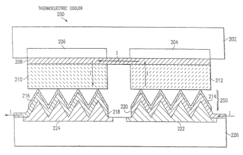
With reference to Figure 2, a cross sectional view of a thermoelectric
cooler with enhanced structured interfaces is depicted in accordance with the
present invention. Thermoelectric cooler 200 inciudes a heat source 226 from
which, with current I flowing as indicated, heat is extracted and delivered
to heat sink 202. Heat source 226 may be thermally coupled to a substance
that is desired to be cooled. Heat sink 202 may be thermally coupled to
devices such as, for example, a heat pipe, fins, and/or a condensation unit
to dissipate the heat removed from heat source 226 and/or further cool heat
source 226.
Heat source 226 is comprised of p- type doped silicon. Heat source 226
is thermally coupled to n+ type doped silicon regions 224 and 222 of tips
250. N+ type regions 224 and 222 are electrical conducting as well as being
good thermal conductors. Each of N+ type regions 224 and 222 forms a reverse
diode with heat source 226 such that no current flows between heat source 226
and n+ regions 224 and 222, thus providing the electrical isolation of heat
source 226 from electrical conductors 218 and 220.
Heat sink 202 is comprised of p- type doped silicon. Heat sink 202 is
thermally coupled to n+ type doped silicon regions 204 and 206. N+ type
regions 204 and 206 are electrically conducting and good thermal conductors.
Each of N+ type regions 204 and 206 and heat sink 202 forms a reverse diode
so that no current flows between the N+ type regions 204 and 206 and heat
sink 202, thus providing the electrical isolation of heat sink 202 from
electrical conductor 208. More information about electrical isolation of
thermoelectric coolers may be found in U.S. Patent No. US6,222,113 Bl
entitled "Electrically Isolated Ultra-Thin Substrates for Thermoelectric
Coolers" assigned to the International Business Machines Corporation of
Armonk, New York and filed on December 9, 1999.
The need for forming reverse diodes with n+ and p- regions to
electrically isolate conductor 208 from heat sink 202 and conductors 218 and
220 from heat source 226 is not needed if the heat sink 202 and heat source
226 are constructed entirely from undoped non-electrically conducting
silicon. However, it is very difficult to ensure that the silicon is
entirely undoped. Therefore, the presence of the reverse diodes provided by
the n+ and p- regions ensures that heat sink 202 and heat source 226 are
electrically isolated from conductors 208, 218, and 220. Also, it should be
noted that the same electrical isolation using
CA 02427426 2003-04-30
WO 02/47176 PCT/GB01/05188
8
reverse diodes may be created other ways, for example, by using p+ type
doped silicon and n- type doped silicon rather than the p- and n+ types
depicted. The terms n+ and p+, as used herein, refer to highly n doped
and highly p doped semiconducting material respectively. The terms n- and
p-, as used herein, mean lightly n doped and lightly p doped
semiconducting material respectively.
Thermoelectric cooler 200 is similar in construction to
thermoelectric cooler 100 in Figure 1. However, N-type 106 and P-type 104
semiconductor structural interfaces have been replaced with superlattice
thermoelement structures 210 and 212 that are electrically coupled by
electrical conductor 208. Electrical conductor 208 may be formed from
platinum (Pt) or, alternatively, from other conducting materials, such as,
for example, tungsten (W), nickel (Ni), or titanium copper nickel
(Ti/Cu/Ni) metal films.
A superlattice is a structure consisting of alternating layers of
two different semiconductor materials, each several nanometers thick.
Thermoelement 210 is constructed from alternating layers of N-type
semiconducting materials and the superlattice of thermoelement 212 is
constructed from alternating layers of P-type semiconducting materials.
Each of the layers of alternating materials in each of thermoelements 210
and 212 is 10 nanometers (nm) thick. A superlattice of two semiconducting
materials has lower thermal conductivity, A, and the same electrical
conductivity, a, as an alloy comprising the same two semiconducting
materials.
In one embodiment, superlattice thermoelement 212 comprises
alternating layers of p-type bismuth chalcogenide materials such as, for
example, alternating layers of Bi2Te3/SbzTe3 with layers of Bio,5Sb1.5Te3, and
the superlattice of thermoelement 210 comprises alternating layers of
n-type bismuth chalcogenide materials, such as, for example, alternating
layers of Bi2Te3 with layers of BixSe3. Other types of semiconducting
materials may be used for superlattices for thermoelements 210 and 212 as
well. For example, rather than bismuth chalcogenide materials, the
superlattices of thermoelements 210 and 212 may be constructed from cobalt
antimony skutteridite materials.
Thermoelectric cooler 200 also includes tips 250 through which
electrical current I passes into thermoelement 212 and then from
thermoelement 210 into conductor 218. Tips 250 includes n+ type
CA 02427426 2003-04-30
WO 02/47176 PCT/GB01/05188
9
semiconductor 222 and 224 formed into pointed conical structures with a
thin overcoat layer 218 and 220 of conducting material, such as, for
example, platinum (Pt). Other conducting materials that may be used in
place of platinum include, for example, tungsten (W), nickel (Ni), and
titanium copper nickel (Ti/Cu/Ni) metal films. The areas between
and around the tips 250 and thermoelectric materials 210 and 212 should be
evacuated or hermetically sealed with a gas such as, for example, dry
nitrogen.
On the ends of tips 250 covering the conducting layers 218 and 220
is a thin layer of semiconducting material 214 and 216. Layer 214 is
formed from a P-type material having the same Seebeck coefficient, a, as
the nearest layer of the superlattice of thermoelement 212 to tips 250.
Layer 216 is formed from an N-type material having the same Seebeck
coefficient, a, as the nearest layer of thermoelement 210 to tips 250.
The P-type thermoelectric overcoat layer 214 is necessary for
thermoelectric cooler 200 to function since cooling occurs in the region
near the metal where the electrons and holes are generated. The n-type
thermoelectric overcoat layer 216 is beneficial, because maximum cooling
occurs where the gradient (change) of the Seebeck coefficient is maximum.
The thermoelectric overcoat 214 for the P-type region is approximately 60
nm thick. A specific thickness of the n-type thermoelectric overcoat 216
has yet to be fully refined, but it is anticipated that it should be in a
similar thickness range to the thickness of the thermoelectric overcoat
214.
By making the electrical conductors, such as, conductors 110 in
Figure 1, into pointed tips 250 rather than a planer interface, an
increase in cooling efficiency is achieved. Lattice thermal conductivity,
A, at the point of tips 250 is very small because of lattice mismatch.
For example, the thermal conductivity, A, of bismuth chalcogenides is
normally approximately 1 Watt/meter*Kelvin. However, in pointed tip
structures, such as tips 250, the thermal conductivity is reduced, due to
lattice mismatch at the point, to approximately 0.2 Watts/meter*Kelvin.
However, the electrical conductivity of the thermoelectric materials
remains relatively unchanged. Therefore, the figure of merit, ZT, may be
increased to greater than 2.5 for this kind of material. Another type of
material that is possible for the superlattices of thermoelements 210 and
212 is cobalt antimony skutteridites. These type of materials typically
have a very high thermal conductivity, .2, making them normally
CA 02427426 2003-04-30
WO 02/47176 PCT/GB01/05188
undesirable. However, by using the pointed tips 250, the thermal
conductivity can be reduced to a minimum and produce a figure of merit,
ZT, for these materials of greater than 4, thus making these materials
very attractive for use in thermoelements 210 and 212. Therefore, the use
5 of pointed tips 250 further increases the efficiency of the thermoelectric
cooler 200 such that it is comparable to vapor compression refrigerators.
Another advantage of the cold point structure is that the electrons
are confined to dimensions smaller than the wavelength (corresponding to
10 their kinetic energy). This type of confinement increases the local
density of states available for transport and effectively increases the
Seebeck coefficient. Thus, by increasing " and decreasing 8, the figure of
merit ZT is increased.
Normal cooling capacity of conventional thermoelectric coolers, such
as illustrated in Figure 1, are capable of producing a temperature
differential, dT, between the heat=source and the heat sink of around 60
Kelvin. However, thermoelectric cooler 200 is capable of producing a
temperature.differential of the order of 150 Kelvin. Thus, with two
thermoelectric coolers coupled to each other, cooling to temperatures in
the range of liquid Nitrogen (less than 100 Kelvin) is possible. However,
different materials may need to be used for thermoelements 210 and 212.
For example, bismuth telluride has a very low a at low temperature (i.e.
less than -100 degrees Celsius). However, bismuth antimony alloys perform
well at low temperature.
Another advantage of the cobalt antimony skutteridite materials over
the bismuth chalcogenide materials, not related to temperature, is the
fact that the cobalt antimony skutteridite materials are structurally more
stable whereas the bismuth chalcogenide materials are structurally weak.
.Those of ordinary skill in the art will appreciate that the
construction of the thermoelectric cooler in Figure 2 may vary depending
on the implementation. For example, more or fewer rows of tips 250 may be
included than depicted in Figure 1. The depicted example is not meant to
imply architectural limitations with respect to the present invention.
With reference now to Figure 3, a planer view of thermoelectric
cooler 200 in Figure 2 is depicted in accordance with the present
invention. Thermoelectric cooler 300 includes an n-type thermoelectric
material section 302 and a p-t-ype thermoelectric material section 304.
CA 02427426 2003-04-30
WO 02/47176 PCT/GB01/05188
11
Both n-type section 302 and p-type section 304 include a thin layer of
conductive material 306 that covers a silicon body.
Section 302 includes an array of conical tips 310 each covered with
a thin layer of n-type material 308 of the same type as the nearest layer
of the superlattice for thermoelement 210. Section 304 includes an array
of conical tips 312 each covered with a thin layer of p-type material 314
of the same type as the nearest layer of the superlattice for
thermoelement 212.
With reference now to Figures 4A and 4B, a cross sectional views of
tips that may be implemented as one of tips 250 in Figure 2 is depicted in
accordance with the present invention. Tip 400 includes a silicon cone
that has been formed with a cone angle of approximately 35 degrees. A
thin layer 404 of conducting material, such as platinum (Pt), overcoats
the silicon 402. A thin layer of thermoelectric material 406 covers the
very end of the tip 400. The cone angle after all layers have been
deposited is approximately 45 degrees. The effective tip radius of tip
400 is approximately 50 nanometers.
Tip 408 is an alternative embodiment of a tip, such as one of tips
250. Tip 408 includes a silicon cone 414 with a conductive layer 412 and
thermoelectric material layer 410 over the point. However, tip 408 has a
much sharper cone angle than tip 400. The effective tip radius of tip 408
is approximately 10 nanometers. It is not known at this time whether a
broader or narrower cone angle for the tip is preferable. In the present
embodiment, conical angles of 45 degrees for the tip, as depicted in
Figure 4A, have been chosen, since such angle is in the middle of possible
ranges of cone angle and because such formation is easily formed with
silicon with a platinum overcoat. This is because a KOH etch along the
100 plane of silicon naturally forms a cone angle of 54 degrees. Thus,
after the conductive and thermoelectric overcoats have beerz added, the
cone angle is approximately 45 degrees.
With reference now to Figure 5, a cross sectional view illustrating
the temperature field of a tip near to a superlattice is depicted in
accordance with the present invention. Tip 504 may be implemented as one
of tips 250 in Figure 2. Tip 504 has an effective tip radius, a, of 30-50
nanometers. Thus, the temperature field is localized to a very small
distance, r, approximately equal to 2a or around 60-100 nanometers.
Therefore, a superlattice 502 needs to be only a few layers thick with a
CA 02427426 2003-04-30
WO 02/47176 PCT/GB01/05188
12
thickness, d, of around 100 nanometers. Therefore, using pointed tips, a
thermoelectric cooler with only 5-10 layers for the superlattice is
sufficient.
Thus, fabricating a thermoelectric cooler, such as, for example,
thermoelectric cooler 200, is not extremely time consuming, since only a
few layers of the superlattice must be formed rather than'numerous layers
which can be very time consuming. Thus, thermoelectric cooler 200 can be
fabricated very thin (of the order of 100 nanometers thick) in contrast to
prior art thermoelectric coolers which were of the order of 3 millimeters
or greater in thickness.
Other advantages of a thermoelectric cooler with pointed tip
interfaces in accordance with the present invention include minimization
of the thermal conductivity of the thermoelements, such as thermoelements
210 and 212 in Figure 2, at the tip interfaces. Also, the
temperature/potential drops are localized to an area near the tips,
effectively achieving scaling to sub-100-nanometer lengths. Furthermore,
using pointed tips minimizes the number of layers for superlattic.e growth
2D by effectively reducing the thermoelement lengths. The present invention
also permits electrodeposition of thin film structures and avoids
flip-chip bonds. The smaller dimensions allow for monolithic integration
of n-type and p-type thermoelements.
The thermoelectric cooler of the present invention may be utilized
to cool items, such as, for example, specific spots within a main frame
computer, lasers, optic electronics, photodetectors, and PCR in genetics.
With reference now to Figure 6, a cross sectional view of a
thermoelectric cooler with enhanced structured interfaces with all metal
tips is depicted in accordance with the present invention. Although the
present invention has been described above as having tips 250 constructed
from silicon cones constructed from the n+ semiconducting regions 224 and
222, tips 250 in Figure 2 may be replaced by tips 650 as depicted in
Figure 6. Tips 650 have all metal cones 618 and 620. In the depicted
embodiment, cones 618 and 620 are constructed from copper and have a
nickel overcoat layer 660 and 662. Thermoelectric cooler 600 is identical
to thermoelectric cooler 200 in all other respects, including having a
thermoelectric overcoat 216 and 214 over the tips 650. Thermoelectric
cooler 600 also provides the same benefits as thermoelectric cooler 200.
However, by using all metal cones rather than silicon cones covered with
conducting material, the parasitic resistances withixa the cones become
CA 02427426 2003-04-30
WO 02/47176 PCT/GB01/05188
13
very low, thus further increasing the efficiency of thermoelectric cooler
600 over the already increased efficiency of thermoelectric cooler 200.
The areas surrounding tips 650 and between tips 650 and thermoelectric
materials 210 and 212 should be vacuum or hermetically sealed with a gas,
such as, for example, dry nitrogen.
Also, as in Figure 2, heat source 226 is comprised of p- type doped
silicon. in contrast to Figure 2, however, heat source 226 is thermally
coupled to n+ type doped silicon regions 624 and 622 that do not form part
of the tipped structure 650 rather than to regions that do form part of
the tipped structure as do regions 224 and 222 do in Figure 2. N+ type
doped silicon regions 624 and 622 do still perform the electrical
isolation function performed by regions 224 and 222 in Figure 2.
Several methods may be utilized to form the all metal cones as
depicted in Figure 6. For example, with reference now to Figure 7, a
cross-sectional view of a sacrificial silicon template that may be used
for forming all metal tips is depicted in accordance with the present
invention. _After the sacrificial silicon template 702 has been
constructed having conical pits, a layer of metal may be deposited over
the template 702 to produce all metal cones 704. All metal cones 704 may
then be used in thermoelectric cooler 600.
With reference now to Figure 8, a flowchart illustrating an
exemplary method of producing all metal cones using a silicon sacrificial
template is depicted in accordance with the present invention. To begin,
conical pits are fabricated by anisotropic etching of silicon to create a
mold (step 802). This may be done by a combination of KOH etching,
oxidation, and/or focused ion-beam etching. Such techniques of
fabricating a silicon cone are well known in the art.
The silicon sacrificial template is then coated with a thin
sputtered layer of seed metal, such as, for example, titanium or platinum
(step 804). Titanium is preferable since platinum forms slightly more
rounded tips than titanium, which is very conforming to the conical pits.
Next, copper is electrochemically deposited to fill the valleys (conical
pits) in the sacrificial silicon template. (step 806). The top surface of
the copper is then planarized (step 808). Methods of planarizing a layer
of metal are well known in the art. The silicon substrate is then removed
by selective etching methods well known in the art (step 810). The all
metal cones produced in this manner may then be covered with a coat of
another metal, such as, for example, nickel or titanium and then with an
CA 02427426 2003-04-30
WO 02/47176 PCT/GB01/05188
14
ultra-thin layer of thermoelectric material. The nickel or titanium
overcoat aids in electrodeposition of the thermoelectric material
overcoat.
[One advantage to this method of producing all metal cones is that
the mold that is produced is reusable. The mold may be reused up to
around 10 times before the mold degrades and becomes unusable.] Forming a
template in this manner is very well controlled and produces very uniform
all metal conical tips since silicon etching is very predictable and can
calculate slopes of the pits and sharpness of the cones produced to a very
few nanometers.
Other methods of forming all metal cones may be used as well. For
example, with reference now to Figure 9, a cross sectional view of all metal
cones 902 formed using patterned photoresist is depicted in accordance with
the present invention. rn this method, a layer of metal is formed over the
bottom portions of a partially fabricated thermoelectric cooler. A
patterned photoresist 904-908 is then used to fashion all metal cones 902
with a direct electrochemical etching method.
With reference now to Figure 10, a flowchart illustrating an exemplary
method of forming all metal cones using photoresist is depicted in
accordance with the present invention. To begin, small sections of
photoresist are patterned over a metal layer, such as copper, of a partially
fabricated thermoelectric cooler, such as thermoelectric cooler 600, in
Figure 6 (step 1002). The photoresist may be patterned in an array of
sections having photoresist wherein each area=of photoresist within the
array corresponds to areas in which tips to the all metal cones are desired
to be formed. The metal is then directly etched electrochemically (step
1004) to produce cones 902 as depicted in Figure 9. The photoresist is then
removed and the tips of the all metal cones may then be coated with another
metal, such as, for example, nickel (step 1006). The second metal coating
over the all metal cones may then be coated with an ultra-thin layer of
thermoelectric material (step 1008). Thus, all metal cones with a
thermoelectric layer on the tips may be formed which may used in a
thermoelectric device, such as, for example, thermoelectric cooler 600. The
all metal conical points produced in this manner are not as uniform as those
produced using the method illustrated in Figure 8. However, this method
currently is cheaper and therefore, if cost is an important factor, may be a
more desirable method.
CA 02427426 2003-04-30
WO 02/47176 PCT/GB01/05188
The depicted methods of fabricating all metal cones are merely
examples. Other methods may be used as well to fabricate all metal cones
for use with thermoelectric coolers. Furthermore, other types of metals
may be used for the all metal cone other than copper.
5
With reference now to Figure 11, a cross-sectional view of a
thermoelectric cooler with enhanced structural interfaces in which the
thermoelectric material rather than the metal conducting layer is formed
into tips at the interface is depicted in accordance with the present
10 invention. Thermoelectric cooler 1100 includes a cold plate 1116 and a
hot plate 1102, wherein the cold plate is in thermal contact with the
substance that is to be cooled. Thermal conductors 1114 and 1118 provide
a thermal couple between electrical conducting plates 1112 and 1120
respectively. Thermal conductors 1114 and 1118 are constructed of heavily
15 n doped (n+) semiconducting material that provides electrical isolation
between cold plate 1116 and conductors 1112 and 1120 by forming reverse
biased diodes with the p- material of the cold plate 1116. Thus, heat is
transferred from the cold plate 1116 through conductors 1112 and 1120 and
eventually to hot plate 1102 from which it can be dissipated without
allowing an electrical coupling between the thermoelectric cooler 1100 and
the substance that is to be cooled. Similarly, thermal conductor 1104
provides a thermal connection between electrical conducting plate 1108 and
hot plate 1102, while maintaining electrical isolation between the hot
plate and electrical conducting plate 1108 by=forming a reverse biased
diode with the hot plate 1102 p- doped semiconducting material as
discussed above. Thermal conductors 1104 is also an n+ type doped
semiconducting material. Electrical conducting plates 1108, 1112, and
1120 are constructed from platinum (Pt) in this embodiment. However,
other materials that are both electrically conducting and thermally
conducting may be utilized as well. Also, it should be mentioned that the
areas surrounding tips 1130-1140 and between tips 1130-1140 and
thermoelectric materials 1122 and 1110 should be evacuated to produce a
vacuum or should be hermetically sealed with a gas, such as, for example,
dry nitrogen.
In this embodiment, rather than providing contact between the
thermoelements and the heat source (cold end) metal electrode (conductor)
through an array of points in the metal electrode as in Figures 2 and 6,
the array of points of contact between the thermoelement and the metal
electrode is provided by an array of points 1130-1140 in the
thermoelements 1124 and 1126. In the embodiments described above with
CA 02427426 2003-04-30
WO 02/47176 PCT/GB01/05188
16
reference to Figures 2 and=6, the metal electrode at the cold end was
formed over silicon tips or alternatively metal patterns were directly
etched to form all-metal tips. However, these methods required
thermoelectric materials to be deposited over the cold and the hot
electrodes by electrochemical methods. The electrodeposited materials
tend to be polycrystalline and do not have ultra-planar surfaces. Also,
the surface thermoelectric properties may or may not be superior to single
crystalline thermoelectric materials. Annealing improves the
thermoelectric properties of the polycrystalline materials, but surface
smoothness below l00nm roughness levels remains a problem. The tips
1130-1140 of the present embodiment may be formed from single crystal or
polycrystal thermoelectric materials by electrochemical etching.
In one embodiment, thermoelement 1124 is comprised of a super
lattice of single crystalline Bi2Te3/Sb2Te3 and Bio.58b,..5Te3 and
thermoelement
1126 is formed of a super lattice of single crystalline BiZTe3/BiZSej and
Bi2Te2,oSeo.1. Electrically conducting plate 1120 is coated with a thin
layer 1122 of the same thermoelectric material as is the material of the
tips 1130-1134 that are nearest thin layer 1120. Electrically conducting
plate 1112 is coated with a thin layer 1110 of the same thermoelectric
material as is the material of the tips 1136-1140 that are nearest thin
layer 1112.
With reference now to Figure 12, a flowchart illustrating an
exemplary method of fabricating a thermoelectric cooler, such as, for
example, thermoelectric cooler 1100 in Figure 11, is depicted in
accordance with the present invention. Optimized single crystal material
are first bonded to metal electrodes by conventional means or metal
electrodes are deposited onto single crystal materials to form the
electrode connection pattern (step 1202). The other side of the
thermoelectric material 1314 is then patterned (step 1204) by photoresist
1302-1306 as depicted in Figure 13 and metal electrodes are used in an
electrochemical bath as an anode to electrochemically etch the surface
(step 1206). The tips 1308-1312 as depicted in Figure 13 are formed by
controlling and stopping the etching process at appropriate times.
A second single crystal substrate is thinned by chemical-mechanical
polishing and then electrochemically etching the entire substrate to
nanometer films (step 1210). The second substrate with the ultra-thin
substrate forms the cold end and the two substrates (the one with the
ultra-thin thermoelectric material and the other with the thermoelectric
tips) are clamped together with pressure (step 1212). This structure
CA 02427426 2003-04-30
WO 02/47176 PCT/GB01/05188
17
retains high crystallinity in all regions other than the interface at the
tips. Also, the same method can be used to fabricate polycrystalline
structures rather than single crystalline structures.
With reference now to Figure 14, a diagram showing a cold point tip
above a surface for use in a thermoelectric cooler illustrating the
positioning of the tip relative to the surface is depicted in accordance
with the present invention. Although the tips, whether created in as
all-metal or metal coated tips or as thermoelectric tips have been
described thus far as being in contact with the surface opposite the tips.
However, although the tips may be in contact with the opposing surface, it
is preferable that the tips be near the opposing surface without touching
the surface as depicted in Figure 14. The tip 1402 in Figure 14 is
situated near the opposing surface 1404 but is not in physical contact
with the opposing surface. Preferably, the tip 1402 should be a distance
d on the order of 5 nanometers or less from the opposing surface 1404. In
practice, with a thermoelectric cooler containing thousands of tips, some
of the tips may be in contact with the opposing surface while others are
not in contact due to the deviations from a perfect plane of the opposing
surface.
By removing the tips from contact with the opposing surface, the
amount of thermal conductivity between the cold plate and the hot plate of
a thermoelectric cooler may be reduced. Electrical conductivity is
maintained, however, due to tunneling of electrons between the tips and
the opposing surface.
The tips of the present invention have also been described and
depicted primarily as perfectly pointed tips. However, as illustrated in
Figure 14, the tips in practice will typically have a slightly more
rounded tip as is the case with tip 1402. However, the closer to
perfectly pointed the tip is, the fewer number of superlattices needed to
achieve the temperature gradient between the cool temperature of the tip
and the hot temperature of the hot plate.
Preferably, the radius of curvature ro of the curved end of the tip
1402 is of the order of a few tens of nanometers. The temperature
difference between adjacent areas of the thermoelectric material below
surface 1404 approaches zero over a distance of two (2) to three (3) times
the radius of curvature ra of the end of tip 1402. Therefore, only a few
layers of the super lattice 1406-1414 are necessary. Thus, a superlattice
material opposite the tips is feasible when the electrical contact between
CA 02427426 2003-04-30
WO 02/47176 PCT/GB01/05188
18
the hot and cold plates is made using the tips of the present invention.
This is in contrast to the prior art in which to use a superlattice
structure without tips, a superlattice of 10000 or more layers was needed
to have a sufficient thickness in which to allow the temperature gradient
to approach zero. Such a number of layers was impractical, but using only
5 or 6 layers as in the present invention is much more practical.
Although the present invention has been described primarily with
reference to a thermoelectric cooling device (or Peltier device) with
tipped interfaces used for cooling, it will be recognized by those skilled
in the art that the present invention may be utilized for generation of
electricity as well. It is well recognized by those skilled in the art
that thermoelectric devices can be used either in the Peltier mode (as
described above) for refrigeration or in the Seebeck mode for electrical
power generation. Referring now to Figure 15, a schematic diagram of a
thermoelectric power generator is depicted. For ease of understanding and
explanation of thermoelectric power generation, a thermoelectric power
generator according to the prior art is depicted rather than a
thermoelectric power generator utilizing cool point tips of the present
invention. -However, it should be noted that in one embodiment of a
thermoelectric power generator according to the present invention, the
thermoelements 1506 and 1504 are replaced by cool point tips, as for
example, any of the cool point tip embodiments as described in greater
detail above.
In a thermoelectric power generator 1500, rather than running
current through the thermoelectric device from a power source 102 as
indicated in Figure 1, a temperature differential, TH-TL, is created across
the thermoelectric device 1500. Such temperature differential, TH-TL,
induces a current flow, I, as indicated in Figure 15 through a resistive
load element 1502. This is the opposite mode of operation from the mode
of operation described in Figure 1
Therefore, other than replacing a power source 102 with a resistor
1502 and maintaining heat elements 1512 and 1516 and constant temperatures
TH and TL respectively with heat sources QH and QL respectively,
thermoelectric device 1500 is identical in components to thermoelectric
device 102 in Figure 1. Thus, thermoelectric cooling device 1500 utilizes
p-type semiconductor 1504 and n-type semiconductor 1506 sandwiched between
poor electrical conductors 1508 that have good heat conducting properties.
Each of elements 1504, 1506, and 1508 correspond to elements 104, 106, and
108 respectively in Figure 1. Thermoelectric device 1500 also includes
CA 02427426 2005-05-18
AUS000414
19
electrical conductors 1510 and 1514 corresponding to electrical conductors
110 and 114 in Figure 1. More information about thermoelectric electric
power generation may be found in CRC Handbook of Thermoelectrics, edited by
D. M. Rowe, Ph.D., D.Sc., CRC Press, New York, (1995) pp. 479-488 and in
Advanced Engineering Thermodynamics, 2nd Edition, by Adiran Bejan, John Wiley
& Sons, Inc., New York (1997), pp. 675-682.
The present invention has been described primarily with reference to
conically shaped tips, however, other shapes of tips may be utilized as well,
such as, for example, pyramidically shaped tips. In fact, the shape of the
tip does not need to be symmetric or uniform as long as it provides a
discrete set of substantially pointed tips through which electrical
conduction between the two ends of a thermoelectric cooler may be provided.
The present invention has applications to use in any small refrigeration
application, such as, for example, cooling main frame computers, thermal
management of hot chips and RF communication circuits, cooling magnetic heads
for disk drives, automobile refrigeration, and cooling optical and laser
devices.
The description of the present invention has been presented for
purposes of illustration and description, but is not intended to be
exhaustive or limited to the invention in the form disclosed. Many
modifications and variations will be apparent to those of ordinary skill in
the art. The embodiment was chosen and described in order to best explain
the principles of the invention, the practical application, and to enable
others of ordinary skill in the art to understand the invention for various
embodiments with various modifications as are suited to the particular use
contemplated.